Article

Closed-Form Transmitter-Side Extraction of Receiver Resonance and Coupling Coefficient in Series–Series Compensated Wireless Power Transfer

1
Department of Mechanical Engineering, Keimyung University, Daegu 42601, Republic of Korea
2
Department of Electronic Engineering, Keimyung University, Daegu 42601, Republic of Korea
3
Department of Automotive Engineering, Keimyung University, Daegu 42601, Republic of Korea
*
Author to whom correspondence should be addressed.
Appl. Sci. 2026, 16(12), 5928; https://doi.org/10.3390/app16125928
Submission received: 26 May 2026 / Revised: 8 June 2026 / Accepted: 10 June 2026 / Published: 11 June 2026
(This article belongs to the Special Issue Advances in Near-Field Wireless Power Transfer)

Abstract

Series–series (S–S) compensated wireless power-transfer (WPT) systems are increasingly deployed where connector-free and reliable energy delivery is required, but practical monitoring becomes ambiguous when receiver-resonance drift and magnetic-coupling variation produce similar transmitter-side impedance changes. This paper addresses that ambiguity by separating the two effects without receiver-side sensing. During a low-power diagnostic interval, the receiver terminal is briefly placed in open and short states, and only the fundamental phasors of the inverter output voltage and primary current are processed together with the known compensation capacitances. After the open-state measurement identifies the primary self-impedance, the short-state residual is mapped to an affine D ω 2 line; its zero crossing gives the receiver resonant frequency and secondary self-inductance, while its slope gives the mutual inductance and coupling coefficient. The routine is implementable as a start-up or periodic diagnostic function in WPT hardware that already measures the primary voltage and current and can impose the required receiver terminal states; it requires no receiver-side measurement, auxiliary sensing coil, short-loop resistance measurement, or iterative zero-phase search. In simulation, the coupling-coefficient error remained below 0.014 % under receiver-inductance tolerance and mutual-inductance variation. In a prototype, the short-state data followed the predicted linear relation with R 2 = 0.9979 , and the extracted coupling coefficient agreed with the reference within about 5 % . The identified receiver resonance was also used to guide operating-frequency adjustment in a practical power-transfer test.

1. Introduction

Wireless power transfer (WPT) delivers energy across an air gap and is attractive wherever galvanic connectors compromise convenience, reliability, or safety. Magnetically coupled resonant WPT now serves consumer electronics, electric vehicles, implantable devices, underwater vehicles, and industrial equipment, as recent reviews document [1,2]. In a broader wireless-energy context, radio-frequency wireless-powered communication networks (WPCNs) use harvested RF energy to sustain data links; for example, Liu et al. optimized throughput with mobile access points under an energy-causality constraint [3]. Those far-field, information-oriented systems differ from the near-field resonant WPT links considered here, whose objective is efficient power delivery. In these systems, the compensation network governs reactive-power cancelation together with the input impedance, output capability, soft-switching margin, and transfer efficiency. The series–series (S–S) topology is among the most compact and widely used: both coils are tuned by series capacitors, and the resonant tank reduces to a simple equivalent circuit [4,5,6]. Modeling and control studies confirm that switching loss, output regulation, and maximum-efficiency operation depend strongly on the resonant parameters and the operating frequency [7,8]. Reliable operation of such a tank therefore presumes that its resonant parameters remain known during operation, not only at design time.
This simplicity does not make the S–S tank insensitive to parameter variation. Air-gap changes, lateral or angular misalignment, magnetic-material tolerance, and aging reshape the magnetic path, and therefore the mutual inductance M and coupling coefficient k; recent studies on misaligned couplers and weak-coupling pads show that self- and mutual-inductance variation and compact long-air-gap operation can substantially affect transfer efficiency and stability [9,10]. The self-inductances L 1 and L 2 can drift as well, shifting the transmitter or receiver resonant frequency. The difficulty addressed in this paper arises when these two effects occur together. From the transmitter alone, a receiver that has detuned through a shift in L 2 and a receiver whose coupling has changed through a shift in M both alter the primary input impedance, so a monitor referenced to nominal parameters cannot tell the two apart and may read receiver detuning as a genuine coupling change [11,12,13]. This ambiguity is most severe precisely when receiver-side sensing and wireless feedback are unavailable, which is the very situation in which transmitter-side monitoring is most valuable. The problem studied here is therefore the joint identification, from transmitter-side measurements only, of the actual receiver self-inductance L 2 , the mutual inductance M, and the coupling coefficient k as separate quantities, rather than the inference of k from a nominal receiver inductance.
Several transmitter-side and front-end methods have been proposed to cut receiver-side sensing and wireless feedback. Yin et al. estimated the mutual inductance and load resistance of an S–S system from the input voltage and current at a single frequency, and a later frequency-sweep variant addressed load monitoring in weakly coupled S–S systems [14,15]. Digital-control and signal-processing schemes have likewise recovered load resistance, mutual inductance, or receiver-side variables from primary measurements, including DSP-based identification and quadrature-demodulator extraction of the primary first-harmonic phasor [16,17]. Additional recent approaches include harmonic-component estimation of mutual inductance and load resistance without wireless communication or frequency scanning [18], LCC–S identification considering rectifier-load inductance [19], ANN-based mutual-inductance estimation for EV charging [20], time-domain nonlinear-least-squares estimation for SS–IPT [21], universal eigenstate-based identification for arbitrary MC–WPT topologies [22], and observer-based online identification for SS–IPT systems [23]. These methods lighten the feedback burden, but they typically assume known resonator parameters, depend on load-related conditions, fix the operating frequency, or demand nontrivial computation. None provides a closed-form separation of the actual receiver self-inductance L 2 from the mutual inductance M inside the S–S tank.
Faster coupling-coefficient monitoring has been pursued through active-rectifier states, power-factor or zero-phase-angle detection, and frequency sweeping [24,25]. Recent universal-charger schemes estimate both the coupling coefficient and the receiver resonant frequency under unknown receiver conditions, but they add a transmitter-current phase sensor or a sensing coil and locate special in-phase or out-of-phase points through repeated sweeps [26,27]. Other multi-parameter approaches gain compatibility with unknown receivers at the cost of sensing coils, switch-controlled capacitors, or gradient-descent computation [12,13,28]. Harmonic-extraction methods track the mutual inductance without special switching, but they need harmonic extractors and resonator data over frequency, and they lose accuracy under very weak coupling [29]. A tradeoff therefore persists across these works among hardware complexity, assumed receiver information, iterative frequency search, load assumptions, and the recovery of L 2 , M, and k as distinct quantities. The gap that remains is a closed-form, sensor-light procedure that, using only transmitter-side fundamental phasors and without assuming the receiver resonance, separates a receiver-resonance shift from a coupling change and returns L 2 , M, and k individually.
This paper addresses that gap with a closed-form transmitter-side extraction method for the S–S topology with known compensation capacitors, building on the three-mode transmitter-side concept demonstrated previously for an LCC-series system [11]. The main idea is to make the two confounded effects readable as two independent features of a single straight line. The receiver is briefly placed first in an open-terminal state and then in a short-terminal state, and the known compensation capacitances together with only the fundamental phasors of the inverter output voltage V p and the primary current I 1 are used. The open state isolates the primary self-impedance and yields L 1 . In the short state, this primary self-impedance is removed from the measured phasor ratio, and the reflected secondary term is normalized into a quantity D ( ω ) that is affine in ω 2 . The zero crossing of the resulting D ω 2 line fixes the receiver resonant frequency and L 2 , while its slope fixes M and hence k = M / L 1 L 2 . Three features give the method its strength: the receiver resonance and the coupling appear as the zero and the slope of the same line and are therefore separated by construction; the equivalent short-loop resistance cancels algebraically in D ( ω ) , so no receiver-side resistance is measured; and because the construction is closed-form, it requires neither an iterative zero-phase search nor an auxiliary sensing coil or phase sensor.
The main contributions of this paper are summarized as follows.
  • A closed-form transmitter-side formulation is derived in which the receiver self-inductance L 2 , the mutual inductance M, and the coupling coefficient k of an S–S tank are recovered individually from known compensation capacitances and the open- and short-state fundamental phasors, so that L 1 , L 2 , and M are obtained before k is evaluated, rather than k being inferred from a nominal receiver inductance.
  • The receiver-resonance shift and the coupling change are separated by construction, because the normalized quantity D ( ω ) is affine in ω 2 with a zero crossing fixed solely by L 2 and a slope governed by M; the equivalent short-loop resistance cancels in this construction and is never measured.
  • The method is validated both in circuit-level simulation and on a hardware prototype, and the recovered receiver-resonance information is further shown to support operating-frequency selection in a practical power-transfer test.
The remainder of this paper is organized as follows. Section 2 presents the Materials and Methods, deriving the three measurement modes and the normalized quantity D ( ω ) from which L 2 , M, and k are obtained. Section 3 presents the Results, including circuit-level simulation under combined receiver-inductance and coupling variation and hardware-prototype validation with resonance-based operating-frequency adjustment. Section 4 discusses the practical use, strengths, limitations, noise immunity, economic implications, and future directions of the method. Section 5 concludes the paper.

2. Materials and Methods

This section presents the proposed coupling-coefficient extraction method for S–S compensation and derives a closed-form transmitter-side procedure that extracts the primary self-inductance L 1 , secondary self-inductance L 2 , mutual inductance M, and coupling coefficient k from the fundamental phasors of the inverter output voltage V p and primary current I 1 . Single-frequency closed-form formulas can become ill-conditioned near the secondary resonance, where their denominators approach zero. Zero-phase-angle (ZPA) frequency-sweep methods, for their part, generally require identical primary and secondary resonant frequencies to yield a closed-form expression for k. The present method needs neither condition. With the secondary held in a controlled short state, the primary self-impedance is first removed from the measured ratio V p / I 1 ; normalizing the resulting reflected secondary term produces a quantity D ( ω ) that is affine in ω 2 , whose zero gives the secondary resonant frequency and whose slope gives the mutual inductance.
The procedure splits into three measurement modes. Mode 1 places the secondary in an open state and identifies L 1 together with the primary-side equivalent series resistance R 1 . Mode 2 places the secondary in a short state and uses two pre-assigned frequencies within the expected secondary-resonance band to find ω rx and L 2 . Mode 3 keeps the secondary shorted and uses two or more frequencies outside that band to estimate the slope of D ( ω ) , from which M and k follow.

2.1. Target Topology and Frequency Allocation

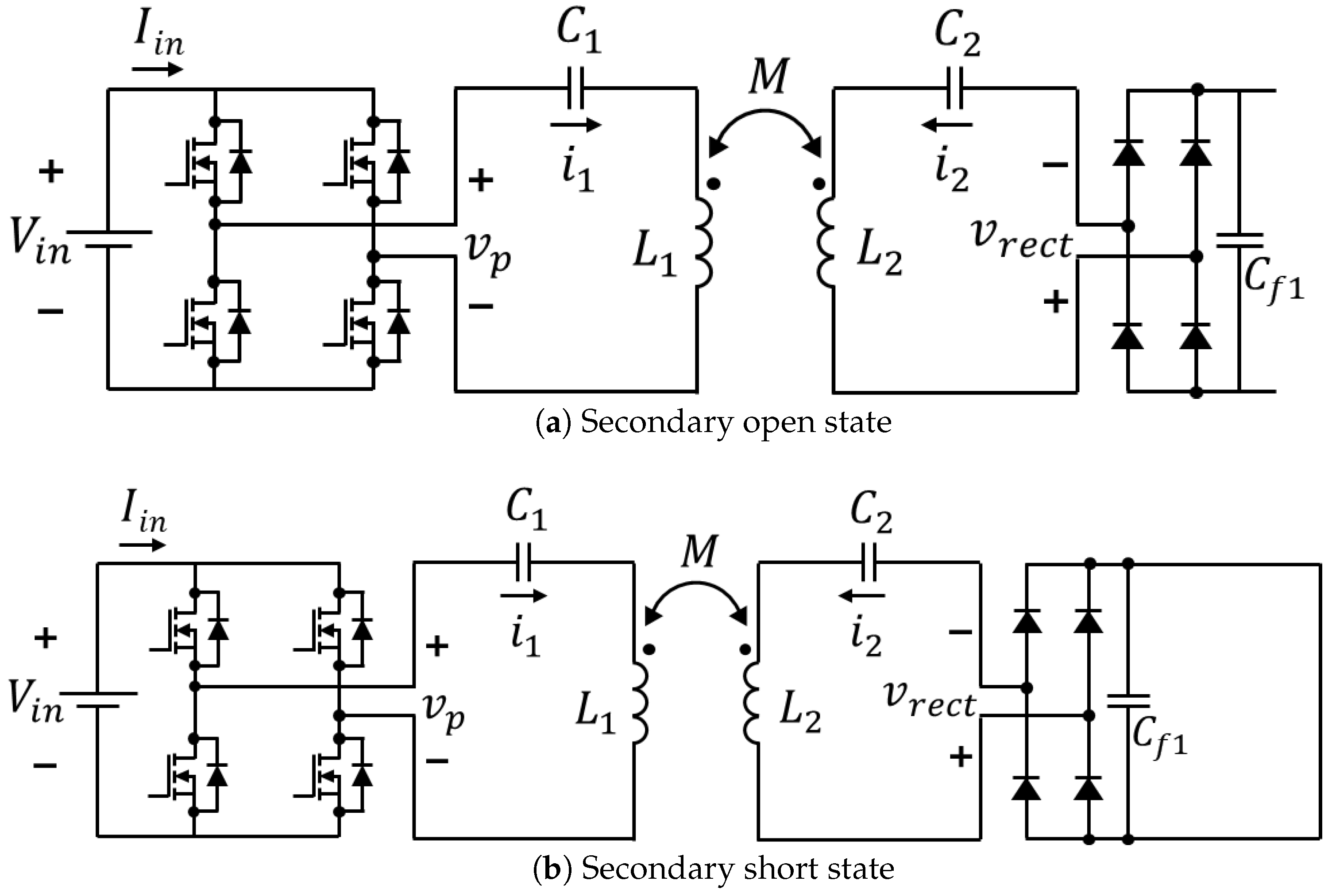
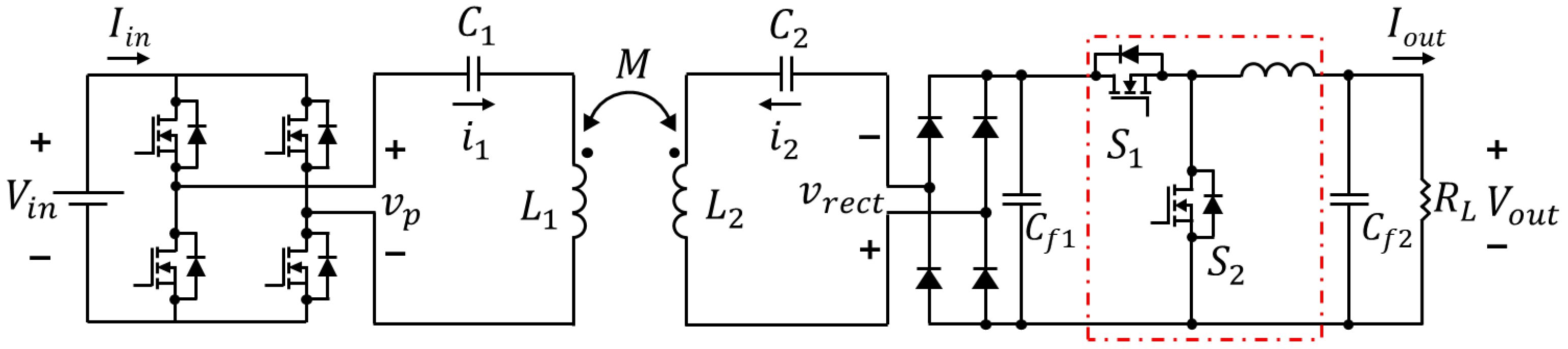
The target system is the S–S compensated wireless power-transfer (WPT) topology shown in Figure 1. The primary side comprises a full-bridge inverter, a series compensation capacitor C 1 , and the transmitter coil L 1 . The secondary side comprises the receiver coil L 2 , a series compensation capacitor C 2 , a diode rectifier, and a back-end load-regulation stage. That stage may be a synchronous buck converter, a bidirectional DC–DC converter, an active rectifier, or any switching topology able to impose open- and short-terminal conditions at the rectifier input; the synchronous buck in Figure 1 is one representative example. In Figure 1, the DC input V i n is inverted into the square-wave voltage v p , which drives the resonant tank through C 1 and L 1 ; the energy coupled to L 2 is rectified onto the filter capacitor C f 1 as v r e c t , and the back-end stage formed by S 1 , S 2 , and C f 2 regulates the output voltage V o u t across the load R L . Of these signals, only the primary-side voltage v p and current i 1 , both marked on the transmitter side, enter the extraction.
In the example circuit of Figure 1, turning off both back-end switches S 1 and S 2 breaks the post-rectifier current path and leaves the rectifier input open. Turning both on ties the rectifier output to a low-impedance loop and creates a short at the rectifier input. In an active-rectifier implementation, the same two terminal states are realized directly through gate control of the rectifier switches. The short state is not a load or battery fault; it is a brief, low-power measurement state in which the load-regulation stage is temporarily detached from the parameter-extraction path. The terminal-state command can be implemented by local receiver firmware, a predefined start-up or diagnostic sequence, or laboratory gate control; the extraction itself still uses only transmitter-side phasors and does not require receiver-side measured quantities to be sent back.

Equivalent Terminal Conditions for the Open and Short States

Figure 2 shows the equivalent secondary terminal conditions used in the measurement modes. These diagrams do not represent the full load-regulation circuit during normal power transfer; they specify only the terminal condition at the rectifier input, which is the sole secondary-side condition the extraction equations require. In the example circuit of Figure 1, the open state corresponds to ( S 1 , S 2 ) = ( 0 , 0 ) and the short state to ( S 1 , S 2 ) = ( 1 , 1 ) . Other back-end topologies are handled identically, provided they can impose the same two rectifier-input conditions. The two states differ in whether the secondary resonant branch carries a fundamental current. In the open state of Figure 2a, the post-rectifier path is broken, so the secondary current is suppressed ( I 2 0 ) and no impedance is reflected to the primary, leaving the primary-side ratio equal to the primary self-impedance alone. In the short state of Figure 2b, the resonant branch is closed through a low-impedance loop, so a secondary current flows and reflects an impedance onto the primary. That reflected impedance is the term carrying the receiver-resonance and coupling information, so Mode 1 uses the open state to fix the primary branch, while Modes 2 and 3 use the short state to recover L 2 and M.
Mode 1 uses the open state of Figure 2a. Once the post-rectifier path is interrupted and the residual DC-link voltage has discharged, the fundamental secondary current satisfies I 2 0 . The primary-side phasor ratio then carries no reflected secondary impedance and reduces to the primary self-impedance,
Z in , oc ( ω ) V p ( ω ) I 1 ( ω ) R 1 + j ω L 1 1 ω C 1 .
Equation (1) is the basis for extracting R 1 and L 1 from primary-side data alone. In practice, residual voltage on the rectifier output capacitor or leakage through the rectifier diodes can weaken I 2 0 ; the DC-link voltage should therefore be verified just before the open-state measurement, or a sufficient discharge interval inserted.
The short state in Figure 2b is used in Modes 2 and 3. It removes the output stage and its control loop from the measurement path while keeping the secondary resonant branch. At the fundamental frequency, the secondary series branch and short loop are
Z 2 , sc ( ω ) = R s + j ω L 2 1 ω C 2 ,
where R s is the equivalent series resistance of the short loop—the receiver-coil resistance, the rectifier conduction resistance, and the on-state resistance of the devices that close the loop. Its numerical value is not needed by the extraction, since it cancels algebraically in the definition of D ( ω ) .
With the secondary impedance reflected through the mutual inductance, the short-state input ratio becomes
Z in , sc ( ω ) V p ( ω ) I 1 ( ω ) = R 1 + j ω L 1 1 ω C 1 + ω 2 M 2 R s + j ω L 2 1 ω C 2 .
Modes 2 and 3 act on the residual left after subtracting the primary self-impedance from this ratio. Combining the real and imaginary parts of that residual forms D ( ω ) , which is linear in ω 2 and free of any separate R s measurement.
Let L 2 , 0 be the design value of the secondary self-inductance and δ L the expected maximum relative variation of L 2 . The actual secondary resonant frequency ω rx = 1 / L 2 C 2 then lies in
Ω rx = 1 C 2 L 2 , 0 ( 1 + δ L ) , 1 C 2 L 2 , 0 ( 1 δ L ) .
The two Mode 2 frequencies ω m , 1 and ω m , 2 are chosen within this interval. The frequencies for Mode 3 mutual-inductance extraction form the set
Ω k = { ω k , 1 , ω k , 2 , , ω k , N k } , N k 2 .
Every element of Ω k lies outside Ω rx and differs from the Mode 1 frequency ω oc . The separation reflects how each mode uses the same line: Mode 2 locates its zero near the secondary resonance, while Mode 3 estimates its slope from points away from resonance, where the noise and safety constraints differ.
For the example circuit, the secondary terminal state is assigned as
( S 1 , S 2 ) = ( 0 , 0 ) , ω = ω oc , ( 1 , 1 ) , ω { ω m , 1 , ω m , 2 } Ω k , normal PWM , ω = ω op .
The pair ( S 1 , S 2 ) applies only to the example in Figure 1; for other back-end topologies, the same rule reads as open state, short state, and normal power-transfer operation at the rectifier input. The extraction occupies brief low-power intervals, and ω op denotes the frequency used for power transfer once the extraction is complete.

2.2. Fundamental-Phasor Synchronous Projection and Measured Quantities

At the nominal resonant frequency, the S–S network attenuates higher-order harmonics. Away from it, the bridge square-wave voltage, the rectifier conduction pattern, and the secondary short state can render the voltage and current waveforms strongly non-sinusoidal. The method therefore avoids RMS values and zero-crossing phase differences, and instead extracts the fundamental phasor at each measurement frequency by synchronous projection.
For a window T m = N c ( 2 π / ω ) with positive integer N c , the synchronous projection of a waveform x ( t ) is
P ω { x } = 2 T m t 0 t 0 + T m x ( t ) e j ω t d t .
When the window spans an integer number of switching cycles, the projection returns the fundamental component at ω and rejects the DC term and the ideal integer harmonics, which are orthogonal over that window. Applied to the two primary-side waveforms—the inverter output voltage v p ( t ) and the primary coil current i 1 ( t ) —it gives
V p ( ω ) = P ω { v p } , I 1 ( ω ) = P ω { i 1 } .
The four measured quantities at each applied frequency are
| V p ( ω ) | , θ v ( ω ) , | I 1 ( ω ) | , θ i ( ω ) .
All extraction formulas use the following real and imaginary components of the measured phasor ratio:
u ( ω ) | V p ( ω ) | | I 1 ( ω ) | cos θ v ( ω ) θ i ( ω ) ,
v ( ω ) | V p ( ω ) | | I 1 ( ω ) | sin θ v ( ω ) θ i ( ω ) .
Thus,
V p ( ω ) I 1 ( ω ) = u ( ω ) + j v ( ω ) .
The quantities u and v are computed directly from the four measurements in (9); no additional impedance transformation is introduced.
To confirm that the fundamental stays dominant at off-resonant points, the current harmonic ratio is evaluated over the same window,
H i ( ω ) = | I 3 ( ω ) | 2 + | I 5 ( ω ) | 2 + | I 7 ( ω ) | 2 | I 1 ( ω ) | ,
where I 3 ( ω ) , I 5 ( ω ) , and I 7 ( ω ) are the third-, fifth-, and seventh-harmonic current phasors obtained by the same projection at 3 ω , 5 ω , and 7 ω . Frequencies for which H i ( ω ) > H max are excluded from the final calculation; the measurement can then be repeated after lowering the input voltage, lengthening the window, or moving closer to the resonant band.

2.3. Derivation of the Linear Relation from the Measurements

This subsection derives D ( ω ) from the measured short-state phasor ratio and shows that, under the fundamental equivalent-circuit model, it is linear in ω 2 .
In the short state, the primary and secondary KVL equations are
V p = R 1 + j ω L 1 1 ω C 1 I 1 + j ω M I 2 ,
0 = j ω M I 1 + R s + j ω L 2 1 ω C 2 I 2 .
The zero on the left-hand side of (15) represents the secondary terminal voltage under the short state: no independent source is connected to the secondary loop, which is driven only by the EMF j ω M I 1 induced through the mutual coupling. Here R s is the equivalent short-loop resistance defined in (2). Its value may vary slightly with frequency, but it does not enter the final extracted parameters because the cancelation is pointwise in frequency.
Solving (15) for the secondary current gives
I 2 = j ω M R s + j ω L 2 1 ω C 2 I 1 .
Substituting (16) into (14) and dividing by I 1 yields
V p ( ω ) I 1 ( ω ) = R 1 + j ω L 1 1 ω C 1 primary self - impedance + ω 2 M 2 R s + j ω L 2 1 ω C 2 reflected secondary impedance .
The first underbraced term is the primary self-impedance, fixed separately in Mode 1, and the second is the secondary branch reflected through the coupling; this reflected term is the only part of the ratio that depends on L 2 , M, and R s , so the remaining steps operate on it alone. Comparing (12) and (17), the real and imaginary parts of the reflected secondary impedance follow from subtracting the primary self-impedance from the measured phasor ratio. Define
A ( ω ) u ( ω ) R 1 ,
B ( ω ) v ( ω ) ω L 1 + 1 ω C 1 .
These residuals depend only on the measured quantities u and v, the primary parameters obtained in Mode 1, the known compensation capacitance C 1 , and the applied frequency.
Let
X 2 ω L 2 1 ω C 2 .
Multiplying the reflected term in (17) by the conjugate of R s + j X 2 gives
ω 2 M 2 R s + j X 2 = ω 2 M 2 ( R s j X 2 ) R s 2 + X 2 2 = ω 2 M 2 R s R s 2 + X 2 2 j ω 2 M 2 X 2 R s 2 + X 2 2 .
Therefore,
A ( ω ) = ω 2 M 2 R s R s 2 + X 2 2 , B ( ω ) = ω 2 M 2 X 2 R s 2 + X 2 2 .
Both residuals share the common factor ω 2 M 2 / ( R s 2 + X 2 2 ) and differ only in whether they retain R s or X 2 ; this shared structure is what lets the normalization below cancel R s exactly. The normalized quantity used by the proposed method is
D ( ω ) ω 3 B ( ω ) A 2 ( ω ) + B 2 ( ω ) .
Dividing by A 2 + B 2 cancels the shared denominator R s 2 + X 2 2 and eliminates R s pointwise; after the remaining frequency powers are balanced by the ω 3 weighting, only the scale factor 1 / M 2 remains, so D is left linear in ω 2 . Substituting (21) into (22) and using
A 2 + B 2 = ω 4 M 4 ( R s 2 + X 2 2 ) ( R s 2 + X 2 2 ) 2 = ω 4 M 4 R s 2 + X 2 2 ,
ω 3 B = ω 3 ω 2 M 2 X 2 R s 2 + X 2 2 = ω 5 M 2 X 2 R s 2 + X 2 2 ,
yields
D ( ω ) = ω 5 M 2 X 2 R s 2 + X 2 2 R s 2 + X 2 2 ω 4 M 4 = ω X 2 M 2 = ω 2 L 2 1 / C 2 M 2 .
Equation (25) has two consequences. First, R s cancels exactly, so the short-loop resistance need not be measured. Second, D ( ω ) is linear in ω 2 . With p ω 2 ,
D = a p + b , a = L 2 M 2 , b = 1 C 2 M 2 .
The zero of this line is
p rx = b a = 1 L 2 C 2 = ω rx 2 ,
which coincides with the secondary series-resonance condition X 2 ( ω rx ) = 0 . Equations (26) and (27) underlie the extraction: Mode 2 reads the zero to obtain ω rx and L 2 , and Mode 3 reads the slope to obtain M.

2.4. Mode 1: Primary Self-Inductance Extraction

Mode 1 runs at ω = ω oc with the secondary open, that is ( S 1 , S 2 ) = ( 0 , 0 ) in the example circuit. Because I 2 0 , the reflected term in (17) vanishes and the phasor ratio becomes
V p ( ω oc ) I 1 ( ω oc ) = R 1 ( ω oc ) + j ω oc L 1 1 ω oc C 1 .
Equating the real and imaginary parts of (12) and (28) gives
u ( ω oc ) = R 1 ( ω oc ) ,
v ( ω oc ) = ω oc L 1 1 ω oc C 1 .
Therefore,
R 1 ( ω oc ) = u ( ω oc ) = | V p ( ω oc ) | | I 1 ( ω oc ) | cos θ v ( ω oc ) θ i ( ω oc ) .
L 1 = 1 ω oc v ( ω oc ) + 1 ω oc C 1 = 1 ω oc | V p ( ω oc ) | | I 1 ( ω oc ) | sin θ v ( ω oc ) θ i ( ω oc ) + 1 ω oc C 1 .
Equation (32) restores the capacitive contribution 1 / ( ω oc C 1 ) to the measured imaginary component. Because the open state removes the reflected term, the imaginary part of the ratio is the reactance of the primary branch alone, so L 1 follows directly from (32) with no coupling contribution. In the following modes, R 1 denotes the resistance value subtracted at the corresponding measurement frequency. If the primary resistance varies appreciably over the measurement band, (31) is repeated in the open state at the relevant frequencies; if the variation is negligible, R 1 ( ω oc ) is used throughout the band.

2.5. Mode 2: Extraction of ω rx and L 2 from Two Measurements

Mode 2 determines the actual secondary resonant frequency ω rx and the corresponding secondary self-inductance L 2 . With the secondary in the short state, the load-regulation stage is removed from the measurement path, and the linear relation in (26) applies. The two frequencies are fixed in advance within the expected resonance interval,
ω m , 1 , ω m , 2 Ω rx , ω m , 1 ω m , 2 ,
so the method, unlike ZPA frequency sweeps that keep adjusting the drive until a zero-phase condition appears, needs only two points to locate the zero crossing of the ideal line.
At each frequency ω m , i for i = 1 , 2 , the four measurements in (9) give u i u ( ω m , i ) and v i v ( ω m , i ) through (10) and (11). The residual components are
A i = u i R 1 , B i = v i ω m , i L 1 + 1 ω m , i C 1 ,
and the corresponding values of D and p are
D i = ω m , i 3 B i A i 2 + B i 2 , p i = ω m , i 2 .
All quantities in (34) and (35) follow from the primary-side phasors, the Mode 1 primary parameters, the known capacitance C 1 , and the applied frequency.
Because the two points ( p 1 , D 1 ) and ( p 2 , D 2 ) lie on D = a p + b ,
D 1 = a p 1 + b ,
D 2 = a p 2 + b ,
Eliminating the intercept b between these two point equations leaves the slope; subtracting these gives a = ( D 2 D 1 ) / ( p 2 p 1 ) , and substituting into p rx = b / a gives
p rx = p 1 D 1 ( p 2 p 1 ) D 2 D 1 ,
or equivalently
p rx = D 2 p 1 D 1 p 2 D 2 D 1 .
Two measurements suffice because the factor 1 / M 2 in (26) scales both D 1 and D 2 equally and therefore cancels in the zero-crossing calculation. The extracted secondary resonant frequency and secondary self-inductance are
ω rx = p rx = D 2 ω m , 1 2 D 1 ω m , 2 2 D 2 D 1 ,
L 2 = 1 C 2 ω rx 2 .
Equation (41) solves the secondary resonance condition ω rx 2 L 2 C 2 = 1 for L 2 , so L 2 is recovered as the actual receiver self-inductance associated with the measured resonance rather than fixed at its design value.
Equation (40) is valid when D 2 D 1 0 . The placement of the two frequencies can also be checked using the signs of D 1 and D 2 : from (26) and (27), D i = a ( p i p rx ) , so the two values have opposite signs when p 1 < p rx < p 2 . Equal signs mean both points sit on the same side of the resonance; the zero can still be extrapolated, but the estimate becomes more sensitive to measurement error, so the pair should be moved to bracket the resonance more closely.
Differentiating (39) with respect to D 1 and D 2 gives
p rx D 1 = D 2 ( p 1 p 2 ) ( D 2 D 1 ) 2 , p rx D 2 = D 1 ( p 2 p 1 ) ( D 2 D 1 ) 2 .
These derivatives show that the estimate becomes noise-sensitive when | D 2 D 1 | is small. The two frequencies should therefore be separated sufficiently, while still satisfying the fundamental-dominance condition in (13).
Because the secondary is short-circuited in Mode 2, the coil current can rise sharply near the secondary resonance, so the primary input voltage must stay below the measurement safety limit. A practical sequence begins at low input voltage, verifies that | I 1 | remains within its rated range, and raises the voltage only until the signal-to-noise ratio is adequate; conservative bounds on k and R s help set a safe voltage range beforehand.

2.6. Mode 3: Mutual Inductance and Coupling-Coefficient Extraction

In Mode 3, the secondary remains short-circuited, and measurements are repeated at the N k 2 frequencies in Ω k . The mutual inductance is then obtained from the slope of the linear relation in (26).
At each measurement frequency ω k , i , Equations (9)–(11) give u k , i and v k , i . The residual components and normalized value are
A k , i = u k , i R 1 ,
B k , i = v k , i ω k , i L 1 + 1 ω k , i C 1 ,
D k , i = ω k , i 3 B k , i A k , i 2 + B k , i 2 , q i = ω k , i 2 .
By (26), the points ( q i , D k , i ) lie on a line whose slope is a = L 2 / M 2 . Mode 3 therefore needs only this slope: the 1 / M 2 factor that canceled out of the Mode 2 zero crossing reappears here as the quantity actually measured. When more than two frequencies are used, the least-squares estimate of the slope is
a k = i = 1 N k ( q i q ¯ ) ( D k , i D ¯ k ) i = 1 N k ( q i q ¯ ) 2 , q ¯ = 1 N k i = 1 N k q i , D ¯ k = 1 N k i = 1 N k D k , i .
Using the Mode 2 result L 2 and the relation a = L 2 / M 2 , the mutual inductance is
M = L 2 a k .
When exactly two frequencies are used, (46) reduces to
a k = D k , 2 D k , 1 q 2 q 1 , M = L 2 ( ω k , 2 2 ω k , 1 2 ) D k , 2 D k , 1 .
Changing the order of the two frequencies reverses the signs of both numerator and denominator in (48), so the slope estimate is independent of ordering. Since a = L 2 / M 2 is positive, a physically consistent measurement should give a k > 0 . A non-positive a k indicates excessive measurement noise, incorrect primary-residual subtraction, or a violation of the assumptions used in deriving (26).
The coupling coefficient is finally calculated as
k = M L 1 L 2 .
The set Ω k is placed outside Ω rx for two reasons. First, from (25), | D | increases as ω 2 moves away from ω rx 2 , so the relative influence of noise on the slope estimate is reduced at off-resonant points. Second, the short-circuit current near the secondary resonance can become large enough to violate the measurement current limit or introduce nonlinear behavior. Frequencies too far from the resonance, however, can amplify inverter harmonics and waveform distortion, so each frequency in Ω k must also satisfy the harmonic criterion in (13).

2.7. Consistency Checks and Overall Procedure

The extracted mutual inductance is checked by evaluating the residual of the linear relation at each Mode 3 point:
ε i D k , i L 2 M 2 ω k , i 2 + 1 C 2 M 2 .
For the model in (26) to be consistent with the measurements, ε i should remain small over the selected frequencies. In addition, the equivalent short-loop resistance recovered from the first relation in (21) is
R s ( ω k , i ) = ω k , i 2 M 2 A k , i A k , i 2 + B k , i 2 .
This value must be positive for a physically valid short-loop model. A large residual in (50) or a negative value in (51) points to an error in the fundamental extraction window, current-sensor phase calibration, primary self-impedance subtraction, or secondary short-state implementation. The corresponding measurement point should then be repeated or excluded.
The complete extraction sequence is as follows. First, the secondary is opened, and the phasor ratio at ω oc gives u ( ω oc ) and v ( ω oc ) through (9); Equations (31) and (32) then give R 1 and L 1 . Second, the secondary is short-circuited and the inverter is driven at ω m , 1 and ω m , 2 ; Equations (34) and (35) give D 1 and D 2 , and (40) and (41) give ω rx and L 2 . Third, with the secondary still short-circuited, the measurement is repeated at the frequencies in Ω k ; Equations (43)–(45) give D k , i , (46) and (47) give M, and (49) gives k.
Because the load is removed during the open- and short-state measurements, the extracted parameters are set by the coupled resonant network rather than by the external load. The synchronous projection keeps non-fundamental waveform components out of the phasor ratio, and the measured L 1 and L 2 are used before M and k are computed. The resulting closed-form sequence can therefore separate a shift in receiver resonance from a change in coupling, even when coil tolerance and positional variation occur together.

2.8. Summary and Significance of the Three Measurement Modes

The complete procedure is summarized in Table 1, which lists, for each mode, the receiver terminal state, the measurement frequencies, the extracted parameters, and the corresponding feature of the D ω 2 line. Read together, the three modes show why a receiver-resonance shift and a coupling change can be separated from transmitter-side data alone.
Mode 1 collapses the input ratio to the bare primary self-impedance, because the open state forces I 2 0 and removes the reflected term. Its significance is that L 1 and R 1 are obtained with no secondary contamination, providing a coupling-free reference that every later mode subtracts; the accuracy of the whole separation is therefore anchored on this single clean measurement.
Mode 2 reads the receiver resonance as the zero crossing of the line. The key insight is that the common factor 1 / M 2 scales every D i equally and so cancels in the ratio of D values that locates the zero in (39); the extracted ω rx and L 2 are thus structurally independent of the coupling. This is the precise reason a coupling change cannot be misread as a receiver-resonance shift, and it also explains why L 2 , being fixed by a zero, tolerates multiplicative scale errors well.
Mode 3 reads the coupling from the slope of the same line, which equals L 2 / M 2 . With L 2 already known from Mode 2, the slope yields M and then k. The insight is complementary to Mode 2: the 1 / M 2 factor that vanished from the zero crossing is exactly what the slope retains, so the coupling is recovered from an orthogonal feature of the same data. Because the zero and the slope are two mathematically independent attributes of one affine relation, a receiver-inductance shift is never charged to the coupling, and a coupling change is never charged to the inductance—the separation is by construction rather than by calibration.
A property shared by all three modes is that the equivalent short-loop resistance R s cancels exactly and pointwise in D ( ω ) , as shown in (25), and therefore never enters the extracted L 2 , M, or k. The three-mode structure thus converts two physically confounded effects into two independent closed-form readings—a zero and a slope—obtained entirely from the transmitter-side fundamental phasors.

3. Results

3.1. Simulation Verification

The proposed method was first verified at the circuit level before any hardware nonideality was introduced. A finite-element coil model supplied the nominal magnetic reference, and these values were embedded in an S–S compensated circuit model. The extraction algorithm operated only on the fundamental phasors of the inverter output voltage and primary current, V p ( ω ) and I 1 ( ω ) ; no receiver-side voltage, current, or impedance was made available to it. This isolates the question the simulation is meant to settle: whether the residual normalization of Section 2 can separate a receiver-resonance shift from a coupling change when both are imposed at once.
The three modes of Section 2 were applied in order. Mode 1 used the open-state receiver condition to identify the primary self-impedance. Mode 2 located the zero crossing of the D ω 2 relation to recover the receiver resonant frequency and self-inductance, and Mode 3 used the slope of the same relation to recover the mutual inductance. The coupling coefficient followed from the extracted L 1 , L 2 , and M through Equation (49).

3.1.1. Finite-Element Coil Model

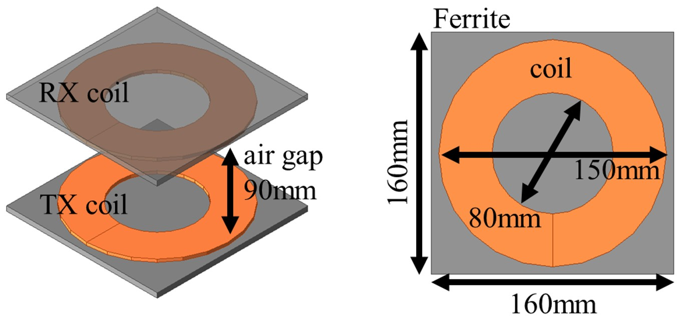
Figure 3 shows the finite-element coil model used to obtain the nominal magnetic reference. The transmitter and receiver coils face each other across a 90 mm air gap, both backed by ferrite plates, with the principal coil and ferrite dimensions marked in the figure. The model was solved at 85 kHz , the nominal receiver-side resonant frequency of the S–S system studied here.
Table 2 lists the setup and the resulting reference values. The nominal transmitter and receiver self-inductances are both 37.0 μ H , and the simulated mutual inductance is 4.14 μ H ; through Equation (49) these give a nominal coupling coefficient k 0 = 0.1119 , rounded to 0.112 in the table.
At k 0 0.112 the magnetic path is weak, so the reflected secondary impedance in Equation (3) is small and strongly frequency-dependent: it grows near the short-circuit secondary resonance and shrinks away from it. This is a demanding setting for the residual step, because any error in the primary self-impedance subtraction propagates directly into A ( ω ) , B ( ω ) , and hence D ( ω ) . A weak-coupling case therefore tests the normalization more severely than a strongly coupled one would.

3.1.2. Simulation Procedure and Error Definition

At each applied frequency the simulated v p ( t ) and i 1 ( t ) were reduced to their fundamental phasors, converted to the real and imaginary parts u ( ω ) and v ( ω ) of Section 2.2, and, after the Mode 1 primary self-impedance was removed, mapped to D ( ω ) through Equation (22). The receiver self-inductance, mutual inductance, and coupling coefficient then followed from the zero crossing and slope of the linear relation in Equation (26).
The finite-element values in Table 2 served as the nominal reference. The additional L 2 and M cases in Section 3.1.4 were imposed parametrically in the circuit model to emulate receiver-coil tolerance and coupling variation; they were used only to compute errors and were never supplied to the extraction. The percentage error of an extracted parameter was defined as
e x = x ^ x ref x ref × 100 % ,
where x ref is the reference value and x ^ the extracted value.

3.1.3. Mode 1 Result: Extraction of L 1 and R 1

Table 3 reports the Mode 1 result under the receiver open-circuit condition. The transmitter self-inductance is recovered as 36.99 μ H against a 37.0 μ H reference, an error of 0.03 % . The primary equivalent resistance is recovered as 0.051 Ω against 0.050 Ω , an error of 2.0 % .
The inductance is accurate enough to anchor the short-state residual. The larger relative error in R 1 reflects only its small magnitude: the absolute discrepancy is 1 m Ω on a 50 m Ω value. Because Modes 2 and 3 subtract the full primary self-impedance before forming the reflected secondary term, this Mode 1 result is the baseline for the rest of the sequence.

3.1.4. Mode 2 and Mode 3 Results: Extraction of L 2 and M

To test the separation directly, the receiver-side parameters were varied in the circuit model. Seven cases were used. Case 1 is the nominal finite-element condition. Cases 2–4 raise the receiver self-inductance by 10 % ( L 2 = 40.7 μ H ) and Cases 5–7 lower it by 10 % ( L 2 = 33.3 μ H ); since C 2 is fixed, each change shifts the receiver series resonance. Within each shifted- L 2 group, M was set to a nominal, a higher, and a lower value, so that coupling varies independently of the inductance tolerance.
Table 4 gives the extracted L 2 and M. Every case recovers L 2 to the displayed precision. The mutual inductance is likewise recovered to the displayed precision except in Case 1, where M ^ = 4.139 μ H against 4.140 μ H , a 0.024 % error. The zero-valued entries should be read as zero error at the printed precision, not as exact recovery.
This pattern is what Equation (26) predicts. The zero crossing of the D ω 2 line sits at p rx = 1 / ( L 2 C 2 ) and is therefore fixed by L 2 alone; the mutual inductance enters only as the common factor 1 / M 2 that scales D, changing the slope but leaving the zero crossing in place. Mode 2 thus returns the correct L 2 for the nominal and the ± 10 % conditions regardless of M. Mode 3 then reads the slope after L 2 is already known, so a receiver-inductance shift is never charged to the coupling, and a coupling change is never charged to the inductance.

3.1.5. Coupling-Coefficient Estimation Result

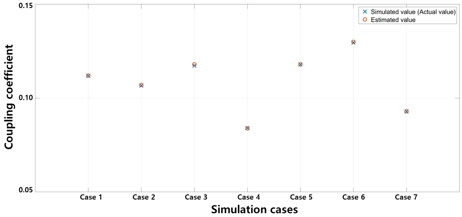
Table 5 and Figure 4 compare the reference and extracted coupling coefficients, computed from the extracted L 1 , L 2 , and M through Equation (49). The largest error is 0.014 % , and the mean is about 0.013 % , and the extracted values track the reference across both the inductance and the coupling variations. The agreement holds because k is formed from the extracted receiver inductance rather than from a nominal value.
The trends follow directly from k = M / L 1 L 2 . Raising L 2 from 37.0 to 40.7 μ H at fixed M = 4.14 μ H lowers the reference k from 0.111892 to 0.106685 , while lowering L 2 to 33.3 μ H raises it to 0.117944 ; the extracted values reproduce both. At fixed L 2 , raising M raises k and lowering M lowers it. Because the method recovers L 2 and M separately, these two influences appear as the distinct effects they are.
The simulation therefore confirms the model-level sequence: Mode 1 fixes the primary self-impedance, Mode 2 recovers the actual receiver inductance even under a ± 10 % resonance shift, Mode 3 recovers the mutual inductance from the slope, and k follows from the extracted inductances and coupling. The coupling-coefficient error stays below 0.014 % throughout. Switching ripple, probe phase error, and nonideal short-state impedance are absent here and are examined next in Section 3.2.

3.2. Experimental Verification

The method was then verified on an S–S compensated WPT prototype to confirm that the sequence of Section 2 survives real switching waveforms rather than only ideal simulation phasors. Only the inverter output voltage v p ( t ) and the primary current i 1 ( t ) were measured; both were reduced to the fundamental phasors V p ( ω ) and I 1 ( ω ) by the synchronous projection of Section 2.2, and no receiver-side quantity entered the extraction.
The open- and short-terminal states were the same as in the method. Mode 1 used the open state to identify the primary self-impedance. For the short state, because the derivation requires only that D ( ω ) be affine in ω 2 , the minimum two-point Mode 2 and two-point Mode 3 calculations were replaced by a single least-squares fit through all measured short-state points. The zero crossing of the fitted line gives the receiver resonance, and its slope gives the mutual inductance. This overdetermined form is the same line as Equation (26); using every point at once averages out oscilloscope quantization, switching ripple, and short-state nonideality. It also permits the short-state frequencies to avoid the immediate high-current neighborhood of the resonance while still bracketing the zero crossing; once the relation is known to be linear, both the zero crossing and the slope can be read from a single fit through well-separated points.

3.2.1. Experimental Prototype and Measurement Conditions

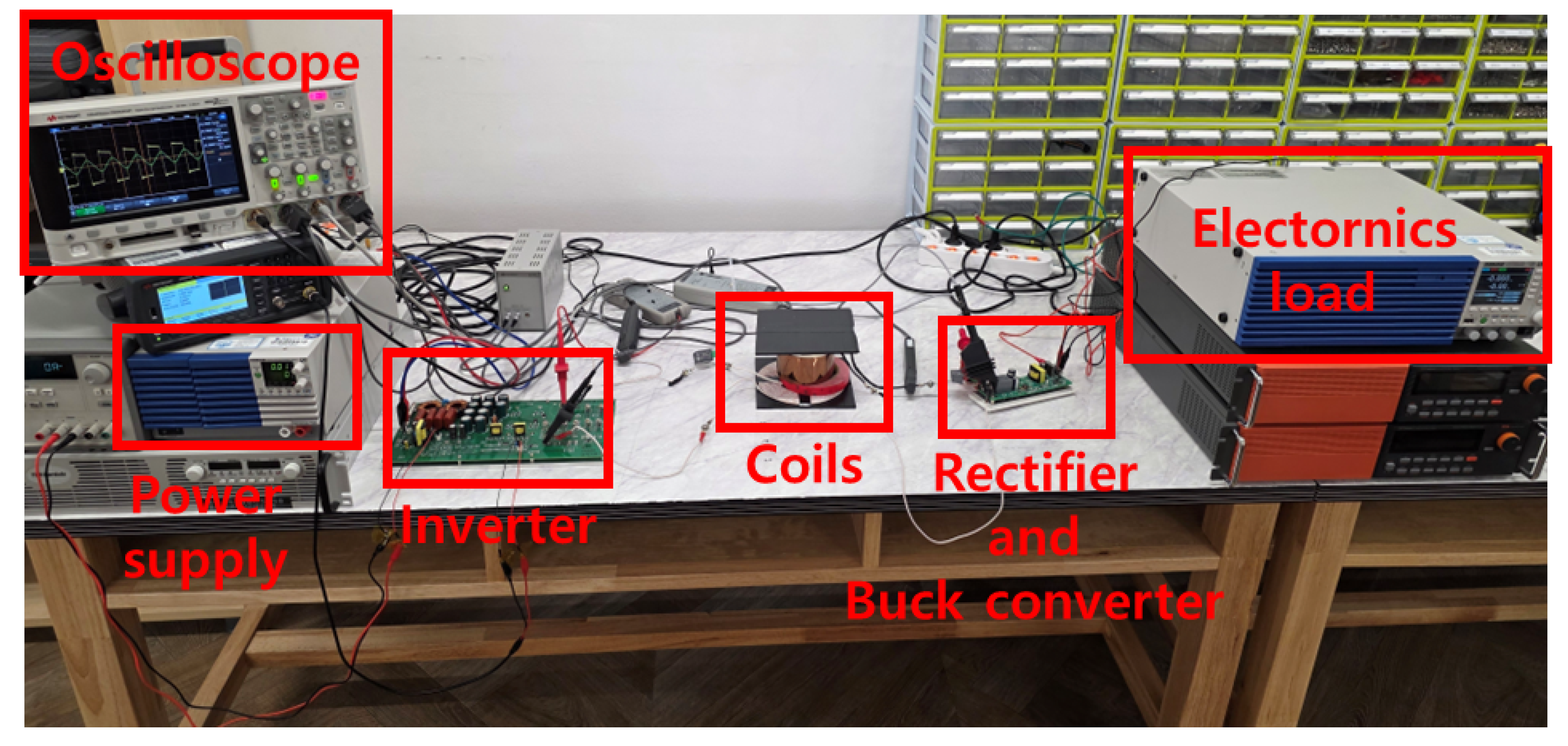
The coils reproduced the finite-element geometry of Figure 3: a 90 mm air gap, ferrite backing, 12 turns, and the same conductor and principal dimensions. Table 6 lists the reference parameters, which were used only to evaluate the extraction error. Figure 5 shows the hardware: a DC power supply, a full-bridge inverter, the coil pair, the rectifier and buck-converter stage that imposes the receiver terminal condition, an electronic load, and the oscilloscope that captured v p ( t ) and i 1 ( t ) at each commanded frequency.
The notation follows Figure 1: L 1 , C 1 form the transmitter branch, L 2 , C 2 the receiver branch, and M , k the magnetic coupling. With the listed reference inductances and mutual inductance, Equation (49) gives k ref = 0.1052 . The coil-resistance entries describe the fabricated coils and are not inputs to the algorithm; the primary equivalent resistance used in the extraction is taken from the Mode 1 open-state ratio.
The short-state sweep points lie below and above the expected receiver resonance and deliberately skip the immediate resonance region, where the short-circuit current is largest. The points at 75 and 95 kHz bracket the zero crossing, and the remaining points extend the lever arm for the slope, in keeping with the safety considerations of Section 2.5.

3.2.2. Measured Waveforms and Fundamental-Phasor Extraction

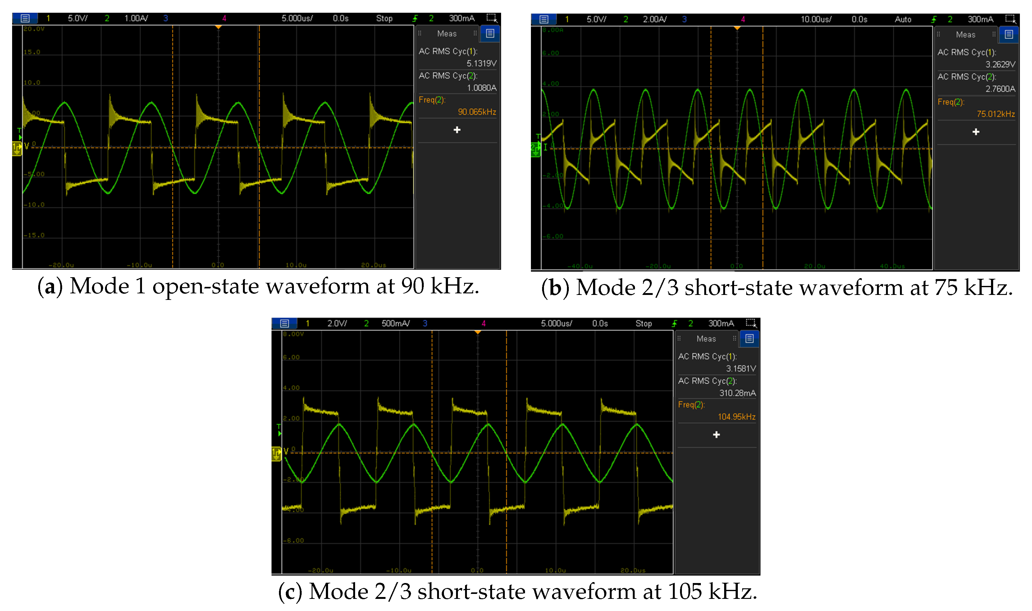
Figure 6 shows representative waveforms: the Mode 1 open state at 90 kHz in (a), and the short state at 75 and 105 kHz in (b) and (c). The bridge voltage carries switching edges and parasitic ringing, and the primary current is visibly non-sinusoidal under off-resonant and short-state operation. RMS magnitudes and zero-crossing phase differences would be unreliable on such waveforms, so each record was projected onto the fundamental at its applied frequency and then converted into u ( ω ) and v ( ω ) .

3.2.3. Mode 1 Result: Primary Self-Impedance Extraction

Table 7 summarizes the Mode 1 result. From the imaginary part of the open-state ratio, the transmitter self-inductance is L ^ 1 = 36.10 μ H against a 35.31 μ H reference, an error of 2.24 % . From the real part, the primary equivalent resistance is R ^ 1 = 0.043 Ω .
The relative error in R 1 is large ( 25.9 % ) because R 1 is a milliohm-level quantity read from the real part of the ratio, where current-probe phase error, inverter dead time, parasitic conduction, and residual non-fundamental components all leave a mark; in absolute terms, the gap is only 15 m Ω . The reference value in Table 7 is the primary-branch equivalent resistance used for model comparison, whereas the coil-resistance entries in Table 6 describe the fabricated windings. Thus, R 1 here should be interpreted as the effective resistance seen by the fundamental-phasor model under the open-state measurement, not as the winding resistance alone. This R 1 uncertainty enters the residual through A ( ω ) in Equation (18), the in-phase part of the reflected term, so it bears mainly on the slope, and hence on M, rather than on the zero crossing. After Mode 1, the measured primary self-impedance was subtracted at each short-state frequency, and D ( ω ) was formed through Equation (22).

3.2.4. Mode 2 and Mode 3 Results: Receiver Resonance and Mutual Inductance

Table 8 lists D ( ω ) at the eight short-state frequencies, scaled by 10 17 . The sign change between 75 and 95 kHz already places the zero crossing near the receiver series resonance.
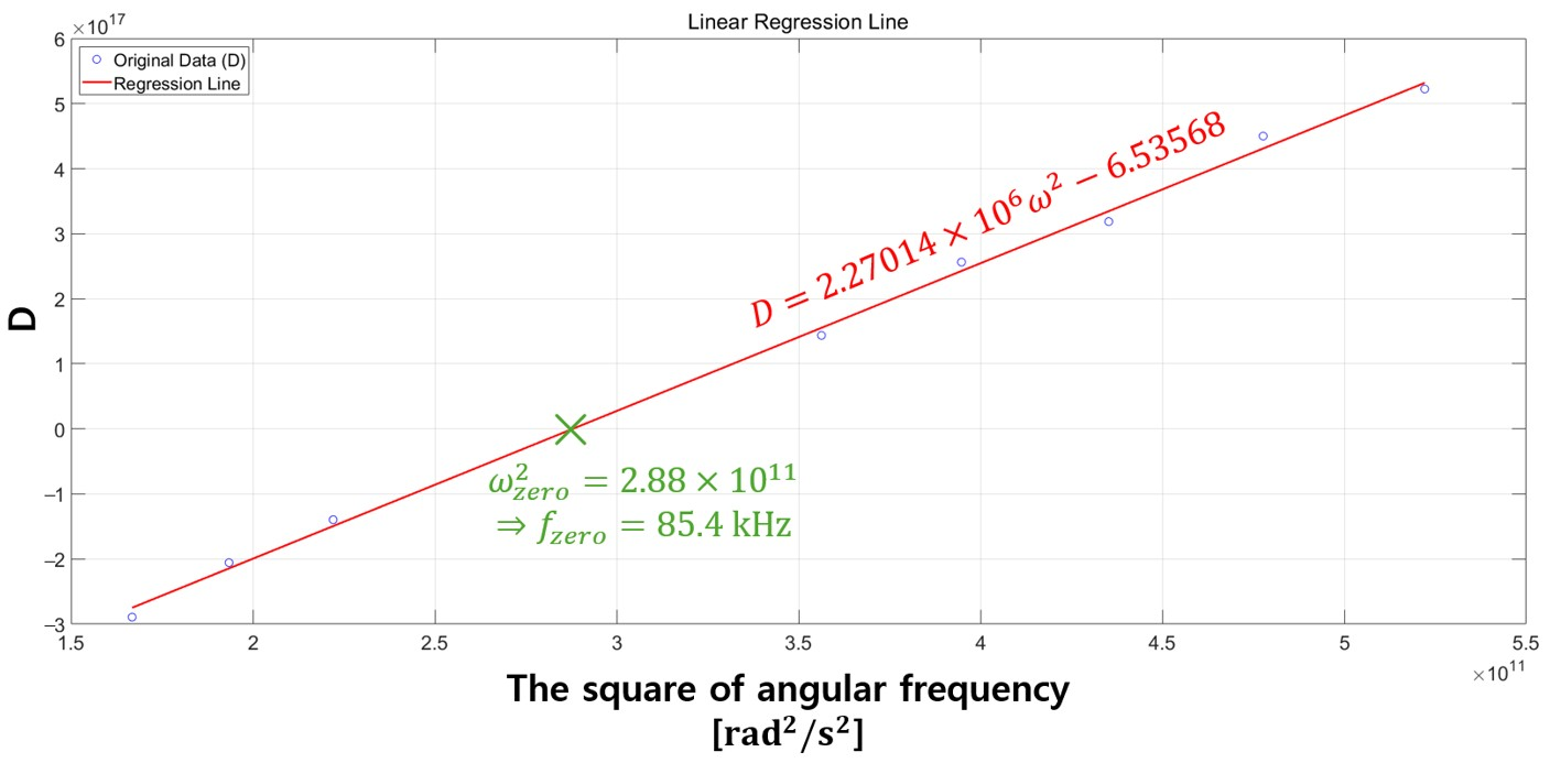
Figure 7 regresses these values against p = ω 2 , giving
D ^ ( p ) = a ^ p + b ^ = 2.27014 × 10 6 p 6.53517 × 10 17 , R 2 = 0.9979 .
The coefficient of determination R 2 = 0.9979 shows that the measured residuals follow the affine law of Section 2.3 closely, despite the switching harmonics, ringing, and short-state nonideality in the raw waveforms. The fit is the overdetermined realization of the single line in Equation (26), not a separate extraction model.
The zero crossing of Equation (53) is p ^ rx = 2.8787 × 10 11 rad 2 / s 2 , that is f ^ rx = 85.39 kHz ; Equation (41) with C 2 = 96.6 nF then gives L ^ 2 = 35.96 μ H . The slope, through Equation (47), gives M ^ = 3.98 μ H .
Table 9 compares these with the reference. The receiver self-inductance error is 0.9 % , and the mutual-inductance error is 5.7 % . The split is expected from the structure of the extraction: the zero crossing in Equation (40) is a ratio of D values in which common multiplicative factors cancel, so it tolerates scale errors well, whereas the slope in Equation (47) carries the absolute magnitude of D and therefore absorbs the R 1 -subtraction, probe-phase, quantization, and short-state errors identified in Section 3.2.3.

3.2.5. Coupling-Coefficient Extraction Result

The coupling coefficient was formed from the extracted inductive parameters, not from a nominal receiver inductance. Equation (49) applied to L ^ 1 = 36.10 μ H , L ^ 2 = 35.96 μ H , and M ^ = 3.98 μ H gives k ^ = 0.1105 , a 5.03 % error against k ref = 0.1052 by Equation (52), as summarized in Table 10.
The result carries the parameter separation into hardware: the receiver inductance came from the zero crossing of the measured D ω 2 line and the mutual inductance from its slope, so k rests on the extracted L 1 , L 2 , and M rather than on an assumed receiver inductance. The error exceeds the simulation figure for the reasons traced in Section 3.2.3 and Section 3.2.4, and is dominated by the slope-based mutual inductance.

3.2.6. Effect of Receiver-Resonance-Based Frequency Adjustment

A separate power-transfer test illustrates how the resonance information can guide the operating point; it is not part of the parameter-extraction error budget. The low-power short-state extraction places the receiver’s intrinsic series resonance at 85.39 kHz , close to its 85 kHz design value. Under load, with the rectifier, buck stage, and output load all active, the best tested operating point of the assembled system lay near 84 kHz . The two values describe different conditions—a diagnostic short-state resonant branch and a loaded power-transfer network—and are therefore not expected to coincide exactly.
Table 11 expands the frequency comparison with the electrical quantities needed to judge the potential application range of the prototype. Here, the transmission voltage denotes the DC input voltage applied to the transmitter inverter, the transferred power denotes the DC load power delivered to R L , and the transmission loss is calculated as P loss = P i n P o u t . The listed 90 mm air gap is the maximum transfer distance evaluated in this prototype, not a fundamental distance limit of the proposed extraction method.
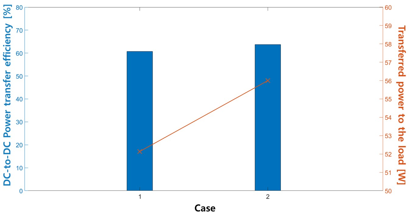
Two operating points were compared on the same hardware. Case 1 fixes the inverter at the nominal 85 kHz receiver resonance, whereas Case 2 uses the resonance-informed loaded operating point of about 84 kHz . At the same 20 V transmitter input and 90 mm air gap, Case 2 increased the transferred load power from 52.1 W to 56.0 W , improved the DC-to-DC efficiency from 60.7 % to 63.7 % , and reduced the transmission loss from 33.8 W to 31.9 W . This corresponds to about a 7.4 % increase in load power, a 3.04 -percentage-point efficiency improvement, and a 5.6 % reduction in loss when calculated from the unrounded measurements.
Figure 8 visualizes the two quantities most directly affected by the operating-frequency adjustment: load power and DC-to-DC efficiency. The extracted intrinsic resonance does not equal the loaded optimum; the value of transmitter-side monitoring is that it makes the relevant resonance information available without receiver-side sensing so that the operating frequency can be selected around measured resonance information rather than from a fixed nominal assumption alone.
The experiment thus supports the full transmitter-side sequence: Mode 1 sets the primary self-impedance baseline; the short-state measurements produce a near-linear D ω 2 relation; its zero crossing yields the receiver self-inductance and its slope the mutual inductance; and k follows from the extracted L 1 , L 2 , and M. The power-transfer comparison further characterizes the present prototype as a 20 V , 50 W -class laboratory WPT link over a maximum tested 90 mm air gap, while remaining separate from the low-power extraction validation.

4. Discussion

4.1. Practical Use, Strengths, Limitations, and Future Research

The method separates a receiver-resonance shift from a coupling change using transmitter-side measurements alone, returning L 1 , L 2 , M, and k as distinct quantities rather than inferring k from a nominal inductance. On the prototype, the measured residuals followed the predicted affine D ω 2 relation with R 2 = 0.9979 , and the extracted coupling matched the reference within about 5 % . Its strengths are that it reuses the inverter output voltage v p and primary current i 1 that the controller already digitizes, adding no sensing coil or receiver-side telemetry; the extraction is closed-form in its minimum two-point implementation and needs no iterative zero-phase search; optional least-squares fitting can also be used when extra points are available for noise averaging; and the receiver resonance and coupling are read as the zero crossing and the slope of one line, separating the two effects by construction.
In practice, the method can run as a coordinated low-power start-up or periodic diagnostic routine in a WPT charger. The receiver back-end imposes the open- and short-terminal states through local firmware, an active rectifier, or a predefined start-up command sequence, while the transmitter records only v p and i 1 ; no receiver-side measured value or cross-coupler measurement feedback is required. For systems whose receiver back-end already supports these terminal states, the method can be added mainly as firmware and calibration logic with little or no added sensing hardware—its practical and scientific value being that quantities otherwise requiring receiver-side measurement become transmitter-side readings. The power-transfer test illustrated the benefit: using measured resonance information to choose the loaded operating frequency raised both the load power and the DC-to-DC efficiency. For application positioning, the present prototype should be interpreted as a low-voltage, approximately 50 W -class WPT link demonstrated at a maximum tested transfer distance of 90 mm ; at the resonance-informed operating point, it delivered 56.0 W at 63.74 % efficiency with 31.86 W loss. A formal evaluation together with a wireless-power-system manufacturer has not yet been undertaken and forms part of the planned industrial validation below.
Several limitations remain. The method needs a receiver back-end that can impose the open- and short-terminal conditions—an active rectifier or a controllable load-regulation stage—so a purely passive diode rectifier cannot use it directly without an added controllable terminal-state path, and its measurement intervals briefly pause power transfer, so it is not yet a continuous in-operation monitor. The short state near the receiver resonance draws a large circulating current, which limits the usable excitation voltage and can reduce the signal-to-noise ratio when all measurement points must be moved farther from resonance for safety. The coupling is the least accurate output, since the slope-derived mutual inductance absorbs the primary-resistance subtraction, current-probe phase, and quantization errors, raising the prototype M error to 5.7 % and the k error to about 5 % . Validation was also confined to a weak-coupling case at a single 90 mm air gap.
Future work includes better primary-side calibration—current-probe phase compensation, inverter dead-time correction, and higher-resolution acquisition—to reduce the mutual-inductance error; a small-signal perturbation overlapping normal power transfer to make the technique a continuous online monitor; broader validation across coupling strength, misalignment, load, and temperature with an industrial pilot to clarify the noise immunity that matters at higher power and longer distance; and extension of the closed-form construction from the S–S tank to topologies such as LCC–S and LCC–LCC, building on the LCC-series formulation that preceded this work [11], broadening the framework to a family of WPT compensation networks.

4.2. Comparison with Existing Transmitter-Side Identification Methods

Transmitter-side parameter identification for S–S WPT has been pursued along two lines, and contrasting their contributions clarifies the gap that the present method fills. The first line estimates the magnetic coupling and often the load while treating the receiver resonance as already known. Yin et al. [14] obtain the mutual inductance and the load resistance from the input voltage and current at a single operating frequency; Yang et al. [24] determine the coupling coefficient within tens of milliseconds through an active-rectifier front end and without any wireless link; Zeng et al. [25] reach sub-one-percent coupling accuracy in a few milliseconds with an adaptive primary-side frequency sweep; and the harmonics-based monitor of [29] tracks the mutual inductance and load movement online, even at the resonant frequency. These schemes are fast and accurate, but each presumes a known receiver resonant frequency, so a detuned, mistuned, or aged receiver lies outside their scope. The second line estimates the receiver resonance jointly with the coupling: the universal-receiver method of [26] and the unknown-parameter S–S method of [27] both return the coupling coefficient together with the receiver resonant frequency, the latter assuming no prior receiver knowledge at all. They reach this richer result through auxiliary sensing—an added transmitter-current phase sensor in [26], and a receiver-coupled sensing coil with a zero-crossing detector in [27]—and through one or two frequency-sweep searches for the zero-phase-angle points.
The proposed method belongs to this second line but removes both of its costs. It extracts the receiver resonance and the coupling from the same transmitter-side fundamental phasors of v p and i 1 that the controller already digitizes—adding no sensing coil, no phase sensor, and no receiver-side telemetry—and it does so in closed form, reading the receiver resonance as the zero crossing and the coupling as the slope of one affine D ω 2 line, so that no iterative zero-phase search is required; the required frequencies are pre-assigned measurement points rather than search results. Table 12 compares the schemes on the capabilities that matter for transmitter-side deployment. Among the surveyed methods, the proposed one is the only scheme that simultaneously extracts both the receiver resonance and the coupling, does not assume nominal receiver inductance or coupling values, adds no auxiliary sensing element, and remains fully closed-form, while using the known compensation capacitances of the tank.
In experimental terms, this architectural simplicity costs little accuracy: the measured coupling-coefficient error of about 5 % is on par with the 4.91 % reported by the closest unknown-receiver method [27], yet the present method needs neither its sensing coil nor its two frequency sweeps. The sweep-based schemes do retain an edge in raw speed, completing within a few milliseconds, and in coupling accuracy down to the sub-one-percent level [25]; the proposed method instead exchanges a brief open- and short-terminal measurement sequence at pre-assigned frequencies for hardware and algorithmic simplicity, which is the more relevant figure of merit when the routine must execute inside an existing transmitter-side controller without added sensing.

4.3. Noise Immunity at Longer Transfer Distances

Because the prototype was characterized at a single 90 mm gap, it is worth stating how the method behaves as the transfer distance grows. A larger gap weakens the coupling, which lowers the reflected secondary contribution relative to the primary self-impedance and thus reduces the signal-to-noise ratio of the short-state measurement—the noise-immunity concern that arises for longer-range industrial links. Two features of the method already counter this. First, every measured quantity is obtained by synchronous fundamental-phasor projection at the known excitation frequency, as in Section 2, so coherent out-of-band switching components are rejected by orthogonality and broadband noise is reduced by averaging the projection over several cycles. Second, in an overdetermined implementation, the receiver resonance and the coupling can be read from a least-squares fit of the affine D ω 2 relation over multiple frequencies, so independent measurement noise is averaged down rather than propagated directly; the prototype fit quality of R 2 = 0.9979 reflects this averaging. For an industrial prototype at longer range, the same robustness is reinforced by standard, low-cost measures—sampling synchronized to the inverter clock, shielded and differential voltage and current sensing, a longer averaging window, and, where needed, repetition of the brief open- and short-terminal sequence—and the residual noise immunity at higher power and distance will be quantified in the planned industrial pilot noted in Section 4.1.

4.4. Economic Considerations for Implementation

The incremental cost is low when the method is applied to regulated WPT hardware that already contains the required terminal-state switches and primary-side voltage/current sensing. On the capital side, it introduces no new power stage in such systems: a transmitter inverter is already present to drive the primary coil, and the receiver commonly contains an output-regulation stage—an active rectifier or a regulated DC–DC converter—for normal charging. In this common regulated case, the stage can place the rectifier input in the open- and short-terminal states the method requires, so no additional sensing coil or measurement-feedback link is needed; systems whose receiver is a purely passive diode rectifier remain excluded unless an additional controllable terminal-state circuit is added, as noted in Section 4.1. The transmitter-side voltage and current used by the method, v p and i 1 , are already digitized by the existing controller for inverter regulation, so no extra primary-side sensors are added either. On the operating side, the routine executes as firmware and calibration logic, requiring only a short open- and short-terminal measurement sequence before normal power transfer resumes. Thus, in compatible regulated platforms, adoption mainly requires firmware integration, calibration, and validation, while the additional energy use and maintenance cost are negligible.

5. Conclusions

This study improved transmitter-side monitoring of S–S compensated WPT by separating receiver-resonance drift from magnetic-coupling variation, rather than estimating k from nominal receiver parameters. Compared with previous transmitter-side and front-end developments that rely on known resonator parameters, auxiliary sensing, phase-sensor information, or iterative frequency searches [14,24,26,27], the proposed method extracts L 1 , L 2 , and M before calculating k. This improvement was achieved using known compensation capacitances and the fundamental phasors of the inverter output voltage and primary current under brief receiver open- and short-terminal states; the open state identifies the primary self-impedance, and the normalized short-state residual D ( ω ) provides f rx and L 2 from its zero crossing and M from its slope.
In simulation, seven cases combining nominal and ± 10 % receiver-inductance variation with different mutual inductances verified this separation. The extracted L 2 matched the reference at the displayed precision in all cases, the maximum M error was 0.024 % , and the coupling-coefficient error remained below 0.014 % . Therefore, a receiver-resonance shift was not misinterpreted as a coupling variation, which is the main improvement over methods that evaluate k using a fixed receiver model.
In the prototype, the measured short-state residuals followed the predicted affine D ω 2 relation with R 2 = 0.9979 . The extracted receiver resonance was f ^ rx = 85.39 kHz , and the extracted parameters were L ^ 2 = 35.96 μ H with 0.9 % error, M ^ = 3.98 μ H with 5.7 % error, and k ^ = 0.1105 with 5.03 % error relative to k ref = 0.1052 . In the power-transfer test, the prototype operated from a 20 V transmitter input across a maximum tested 90 mm air gap and delivered 56.0 W at 63.74 % efficiency when the operating frequency was adjusted to 84 kHz , with 31.86 W transmission loss. The prototype coupling error is comparable to the 4.91 % error reported by the closest unknown-receiver monitoring method, while avoiding its sensing coil and frequency-search steps [27]. These results demonstrate that receiver resonance and coupling coefficient can be obtained in closed form from known compensation capacitances and transmitter-side voltage and current measurements under controlled receiver terminal states, without receiver-side resistance measurement, an auxiliary sensing coil, or iterative zero-phase search.


Author Contributions

Conceptualization, Y.S.; methodology, Y.S. and D.J.; software, D.J.; validation, D.J. and S.W.; formal analysis, D.J. and Y.S.; investigation, D.J. and S.W.; resources, Y.S.; data curation, D.J.; writing—original draft preparation, D.J.; writing—review and editing, Y.S. and S.W.; visualization, D.J.; supervision, Y.S.; project administration, Y.S.; funding acquisition, Y.S. All authors have read and agreed to the published version of the manuscript.

Funding

This research was supported by Korea Institute for Advancement of Technology (KIAT) grant funded by the Korea Government (MOTIE) (P0020536, HRD Program for Industrial Innovation).

Institutional Review Board Statement

Not applicable.

Informed Consent Statement

Not applicable.

Data Availability Statement

The data presented in this study are available on request from the corresponding author.

Acknowledgments

The authors would like to thank ANSYS Korea for the technical support.

Conflicts of Interest

The authors declare no conflict of interest.

References

  1. Abou Houran, M.; Yang, X.; Chen, W. Magnetically coupled resonance WPT: Review of compensation topologies, resonator structures with misalignment, and EMI diagnostics. Electronics 2018, 7, 296. [Google Scholar] [CrossRef] [Scilit]
  2. Okasili, I.; Elkhateb, A.; Littler, T. A review of wireless power transfer systems for electric vehicle battery charging with a focus on inductive coupling. Electronics 2022, 11, 1355. [Google Scholar] [CrossRef] [Scilit]
  3. Liu, X.; Xu, B.; Zheng, K.; Zheng, H. Throughput maximization of wireless-powered communication network with mobile access points. IEEE Trans. Wirel. Commun. 2023, 22, 4401–4415. [Google Scholar] [CrossRef] [Scilit]
  4. Gati, E.; Kokosis, S.; Patsourakis, N.; Manias, S. Comparison of series compensation topologies for inductive chargers of biomedical implantable devices. Electronics 2020, 9, 8. [Google Scholar] [CrossRef] [Scilit]
  5. Wen, F.; Chu, X.; Li, Q.; Gu, W. Compensation parameters optimization of wireless power transfer for electric vehicles. Electronics 2020, 9, 789. [Google Scholar] [CrossRef] [Scilit]
  6. Zhu, Y.; Wu, H.; Li, F.; Zhu, Y.; Pei, Y.; Liu, W. A comparative analysis of S–S and LCCL–S compensation for wireless power transfer with a wide range load variation. Electronics 2022, 11, 420. [Google Scholar] [CrossRef] [Scilit]
  7. Bertolini, V.; Faba, A.; Dionigi, M.; Cardelli, E. Frequency domain model of a resonant LCC–S converter for high-frequency wireless power transfer applications considering switching losses in MOSFETs bridge. Appl. Sci. 2025, 15, 5878. [Google Scholar] [CrossRef] [Scilit]
  8. Wang, X.; Guo, Y.; Wang, R.; Zhang, Y. Coordinated control of constant output voltage and maximum efficiency in wireless power transfer systems. Appl. Sci. 2024, 14, 6546. [Google Scholar] [CrossRef] [Scilit]
  9. Zhang, X.; Wang, X.; Sun, P.; Sun, J.; Cai, J. Mutual and self-inductance variation in misaligned coupler of inductive power transfer system: Mechanism, influence, and solutions. Energies 2023, 16, 5173. [Google Scholar] [CrossRef] [Scilit]
  10. Chen, Y.; Yang, S.; Zheng, M.; Yan, X. Design of inductive power transfer charging system with weak coupling coefficient. Energies 2024, 17, 3836. [Google Scholar] [CrossRef] [Scilit]
  11. Shin, Y.; Woo, S.; Rhee, J.; Lee, C.; Kim, H.; Huh, S.; Park, B.; Ahn, S. Accurate method for extracting the coupling coefficient of an LCC-series wireless power transfer system. IEEE Trans. Power Electron. 2022, 37, 11406–11422. [Google Scholar] [CrossRef] [Scilit]
  12. Xu, L.; Ke, G.; Chen, Q.; Zhang, B.; Ren, X.; Zhang, Z. Multi-parameter estimation for an S/S compensated IPT converter based on the phase difference between Tx and Rx currents. Electronics 2022, 11, 1023. [Google Scholar] [CrossRef] [Scilit]
  13. Liu, C.; Han, W.; Yan, G.; Duan, X. Dual-loop control based receiver resonant frequency tracking and mutual inductance identification in wireless power transfer system. In Proceedings of the IECON 2024–50th Annual Conference of the IEEE Industrial Electronics Society, Chicago, IL, USA, 3–6 November 2024; pp. 1–6. [Google Scholar] [CrossRef] [Scilit]
  14. Yin, J.; Lin, D.; Parisini, T.; Hui, S.Y.R. Front-end monitoring of the mutual inductance and load resistance in a series–series compensated wireless power transfer system. IEEE Trans. Power Electron. 2016, 31, 7339–7352. [Google Scholar] [CrossRef] [Scilit]
  15. Yang, Y.; Jiang, Y.; Tan, S.C.; Hui, S.Y.R. A frequency-sweep based load monitoring method for weakly-coupled series–series compensated wireless power transfer systems. In Proceedings of the 2018 IEEE PELS Workshop on Emerging Technologies: Wireless Power Transfer (WoW), Montreal, QC, Canada, 3–7 June 2018; pp. 1–5. [Google Scholar] [CrossRef] [Scilit]
  16. Shin, H.; Chung, E.; Ha, J.-I. Cost-effective high-performance digital control method in series–series compensated wireless power transfer system. Electronics 2020, 9, 1772. [Google Scholar] [CrossRef] [Scilit]
  17. Trachtenberg, O.; Kuperman, A. Quadrature demodulator-assisted estimation of load voltage and resistance based on primary-side information of a wireless power transfer link. Electronics 2021, 10, 1858. [Google Scholar] [CrossRef] [Scilit]
  18. Yang, D.; Won, S.; Tian, J.; Cheng, Z.; Kim, J. A method of estimating mutual inductance and load resistance using harmonic components in wireless power transfer system. Energies 2019, 12, 2728. [Google Scholar] [CrossRef] [Scilit]
  19. Shen, H.; Wang, X.; Sun, P.; Wang, L.; Liang, Y. Mutual inductance and load identification of LCC-S IPT system considering equivalent inductance of rectifier load. Electronics 2023, 12, 3841. [Google Scholar] [CrossRef] [Scilit]
  20. Abrantes, G.C.; Costa, V.S.; Perdigao, M.S.; Cruz, S. Mutual inductance estimation using an ANN for inductive power transfer in EV charging applications. Energies 2024, 17, 1615. [Google Scholar] [CrossRef] [Scilit]
  21. Mo, L.; Wang, X.; Wang, Y.; Zhang, B.; Jiang, C. Mutual inductance estimation of SS-IPT system through time-domain modeling and nonlinear least squares. Energies 2024, 17, 3307. [Google Scholar] [CrossRef] [Scilit]
  22. Liao, Z.-J.; Gao, B.; Yi, F.; Liu, Z.-P.; Jin, Z.-Y.; Xia, C.-Y. A universal mutual inductance and load identification methodology for MC-WPT systems with arbitrary topology. IEEE Trans. Power Electron. 2024, 39, 16943–16954. [Google Scholar] [CrossRef] [Scilit]
  23. Lee, S.; Lee, S.-H. Observer-based online parameter identification of series-series tuned inductive power transfer system. IEEE Trans. Ind. Electron. 2025, 72, 2927–2937. [Google Scholar] [CrossRef] [Scilit]
  24. Yang, Y.; Tan, S.C.; Hui, S.Y.R. Fast hardware approach to determining mutual coupling of series–series-compensated wireless power transfer systems with active rectifiers. IEEE Trans. Power Electron. 2020, 35, 11026–11038. [Google Scholar] [CrossRef] [Scilit]
  25. Zeng, J.; Chen, S.; Yang, Y.; Hui, S.Y.R. A primary-side method for ultrafast determination of mutual coupling coefficient in milliseconds for wireless power transfer systems. IEEE Trans. Power Electron. 2022, 37, 15706–15716. [Google Scholar] [CrossRef] [Scilit]
  26. Zeng, J.; Yang, Y.; Li, K.; Chen, S.; Hui, S.Y.R. An ultrafast estimation method for coupling coefficient and receiver resonant frequency in universal wireless power transfer systems. IEEE Trans. Power Electron. 2024, 39, 4870–4883. [Google Scholar] [CrossRef] [Scilit]
  27. Zeng, J.; Chen, S.; Li, K.; Hui, S.Y.R. A front-end monitoring method for coupling coefficient and receiver resonant frequency in the SS-compensated wireless power transfer systems with unknown receiver parameters. IEEE Trans. Power Electron. 2024, 39, 6466–6476. [Google Scholar] [CrossRef] [Scilit]
  28. Liu, C.; Han, W.; Hu, Y.; Zhang, B. Simultaneous identification of multiple parameters in wireless power transfer systems using primary variable capacitors. Appl. Sci. 2024, 14, 793. [Google Scholar] [CrossRef] [Scilit]
  29. Zeng, J.; Li, K.; Yuan, H.; Yang, Y.; Tan, S.C.; Parisini, T.; Hui, S.Y.R. A fast front-end monitoring method for mutual inductance and load movement in SS-compensated wireless power transfer systems based on harmonics extraction. IEEE Trans. Power Electron. 2025, 40, 2569–2580. [Google Scholar] [CrossRef] [Scilit]
Figure 1. Example circuit of the S–S compensated WPT system targeted by the proposed method. The red dashed frame indicates the back-end load-regulation stage, which is here implemented as a synchronous buck converter; the same procedure applies to any switching topology, including an active rectifier, that can place the rectifier input either an open or a short state.
Applsci 16 05928 g001
Figure 2. Equivalent secondary terminal conditions used by the proposed method. (a) The post-rectifier current path is interrupted, suppressing the fundamental secondary current. (b) The post-rectifier loop is tied to a low-impedance path, establishing a short-circuit measurement condition at the rectifier input.
Applsci 16 05928 g002
Figure 3. Finite-element coil model used for the simulation verification. The transmitter and receiver coils are separated by a 90 mm air gap, and the coil and ferrite dimensions are indicated in the figure.
Applsci 16 05928 g003
Figure 4. Comparison of the reference and extracted coupling coefficients for the seven simulation cases.
Applsci 16 05928 g004
Figure 5. Experimental hardware setup for the S–S compensated WPT verification. The prototype includes the DC power supply, full-bridge inverter, transmitter and receiver coils, rectifier and buck-converter stage, electronic load, and oscilloscope used for measuring v p ( t ) and i 1 ( t ) .
Applsci 16 05928 g005
Figure 6. Representative experimental waveforms used for transmitter-side phasor extraction. The measured inverter output voltage and primary current are projected onto the fundamental component at each applied frequency before evaluating V p ( ω ) / I 1 ( ω ) .
Applsci 16 05928 g006
Figure 7. Experimental regression of D ( ω ) with respect to ω 2 . The zero crossing gives the receiver resonant frequency, and the slope gives the mutual inductance after using the extracted receiver self-inductance.
Applsci 16 05928 g007
Figure 8. Comparison of DC-to-DC power-transfer efficiency and transferred load power for nominal-frequency operation and resonance-informed frequency adjustment. Case 1 operates at 85 kHz by assuming the nominal receiver resonance, whereas Case 2 operates at the resonance-informed loaded operating frequency of approximately 84 kHz .
Applsci 16 05928 g008
Table 1. Summary of the three measurement modes and their role in the closed-form extraction.
ModeReceiver StateMeasurement FrequenciesExtracted ParametersFeature of the D ω 2 Line
Mode 1Open, ( S 1 , S 2 ) = ( 0 , 0 ) Single point ω oc R 1 , L 1 [Equations (31) and (32)]Reflected term absent; sets the primary self-impedance baseline
Mode 2Short, ( S 1 , S 2 ) = ( 1 , 1 ) ω m , 1 , ω m , 2 Ω rx (≥2 points near resonance) ω rx , L 2 [Equations (40) and (41)]Zero crossing; independent of M
Mode 3Short, ( S 1 , S 2 ) = ( 1 , 1 ) Ω k outside Ω rx (≥2 points off resonance)M, k [Equations (47) and (49)]Slope = L 2 / M 2 ; carries the coupling
Table 2. Finite-element magnetic-simulation setup and nominal reference parameters.
ParameterValue
Air gap between TX and RX coils 90 mm
Simulation frequency 85 kHz
Number of turns per coil12
Conductor diameter 2.8 mm
Nominal TX self-inductance, L 1 , 0 37.0 μ H
Nominal RX self-inductance, L 2 , 0 37.0 μ H
Estimated coil resistance 50 m Ω
Nominal mutual inductance, M 0 4.14 μ H
Nominal coupling coefficient, k 0 0.112
Table 3. Mode 1 open-circuit extraction results.
ParameterReference ValueExtracted ValueError
Primary self-inductance, L 1 37.0 μ H 36.99 μ H 0.03 %
Primary equivalent resistance, R 1 0.050 Ω 0.051 Ω 2.0 %
Table 4. Mode 2 and Mode 3 extraction results for L 2 and M. All inductance values are in μ H .
CaseSimulation Condition L 2 , ref L ^ 2 e L 2 M ref M ^ e M
Case 1Nominal L 2 , nominal M37.037.0 0.000 % 4.1404.139 0.024 %
Case 2 L 2 = 1.1 L 2 , 0 , nominal M40.740.7 0.000 % 4.1404.140 0.000 %
Case 3 L 2 = 1.1 L 2 , 0 , higher M40.740.7 0.000 % 4.5504.550 0.000 %
Case 4 L 2 = 1.1 L 2 , 0 , lower M40.740.7 0.000 % 3.2603.260 0.000 %
Case 5 L 2 = 0.9 L 2 , 0 , nominal M33.333.3 0.000 % 4.1404.140 0.000 %
Case 6 L 2 = 0.9 L 2 , 0 , higher M33.333.3 0.000 % 4.5504.550 0.000 %
Case 7 L 2 = 0.9 L 2 , 0 , lower M33.333.3 0.000 % 3.2603.260 0.000 %
Table 5. Reference and extracted coupling coefficients.
Case k ref k ^ Error
Case 10.1118920.111880 0.011 %
Case 20.1066850.106699 0.013 %
Case 30.1172500.117266 0.014 %
Case 40.0840080.084019 0.013 %
Case 50.1179440.117960 0.014 %
Case 60.1296250.129642 0.013 %
Case 70.0928740.092887 0.014 %
Table 6. Experimental setup parameters. Symbols follow Figure 1; f sc denotes the short-state sweep frequencies used for the overdetermined Mode 2/3 extraction.
GroupSymbolValue
GeometryCoil/ferrite layoutSame as Figure 3
d airgap 90 mm
Number of turns, N 1 , N 2 12, 12
Litz wire 2.8 mm diameter, 0.05 mm × 1300 strands
Reference parameters f ref 85 kHz
L 1 , R 1 , coil 35.31 μ H , 75 m Ω
L 2 , R 2 , coil 36.29 μ H , 78 m Ω
M ref , k ref 3.765 μ H , 0.1052
Compensation C 1 ; nominal TX resonance 112 nF ; 80 kHz
C 2 ; nominal RX resonance 96.6 nF ; 85 kHz
Measurement f oc 90 kHz
f sc 65, 70, 75, 95, 100, 105, 110, and 115 kHz
Table 7. Mode 1 open-state extraction results in the hardware experiment.
ParameterReference ValueExtracted ValueError
Primary self-inductance, L 1 35.31 μ H 36.10 μ H 2.24 %
Primary equivalent resistance, R 1 0.058 Ω 0.043 Ω 25.9 %
Table 8. Measured short-state values of D ( ω ) . The second column is scaled by 10 17 .
Frequency, f [kHz] D ( ω ) [ 10 17 ]
65 2.892
70 2.056
75 1.396
95 1.437
100 2.564
105 3.185
110 4.500
115 5.224
Table 9. Mode 2 and Mode 3 extraction results in the hardware experiment.
ParameterReference ValueExtracted ValueError
Secondary self-inductance, L 2 36.29 μ H 35.96 μ H 0.9 %
Mutual inductance, M 3.765 μ H 3.98 μ H 5.7 %
Table 10. Experimental coupling-coefficient estimation result.
k ref k ^ Error
0.10520.1105 5.03 %
Table 11. Power-transfer operating conditions and measured electrical results. The table reports the transmit-side DC-bus voltage, transferred power, maximum tested transfer distance, and transmission loss for the two operating-frequency cases.
QuantityCase 1: Nominal-Frequency OperationCase 2: Resonance-Informed Operation
Operating frequency 85 kHz 84 kHz
Selection basisNominal RX resonanceBest tested loaded point selected using measured resonance information
DC input voltage, V i n 20.0 V 20.0 V
Maximum tested transfer distance, d airgap 90 mm 90 mm
Input current, I i n 4.3 A 4.4 A
Input power, P i n 85.9 W 87.9 W
Load voltage, V o u t 9.8 V 10.2 V
Load current, I o u t 5.3 A 5.5 A
Transferred load power, P o u t 52.1 W 56.0 W
Transmission loss, P loss = P i n P o u t 33.8 W 31.9 W
DC-to-DC efficiency, η 60.7 % 63.7 %
Table 12. Comparison of transmitter-side parameter-identification schemes for S–S compensated WPT. A marks a capability the scheme provides and × marks one it does not; f rx is the receiver resonant frequency, M the mutual inductance, k the coupling coefficient, and R L the load resistance. The proposed method assumes the compensation capacitances are known.
CriterionYin [14]Yang [24]Zeng [25]Zeng [26]Zeng [27]This Work
Extracted parametersM, R L kkk, f rx k, f rx f rx , M, k
Receiver resonance and coupling both extracted×××
No nominal L 2 or f rx assumption××
No auxiliary sensing element beyond primary voltage/current sensing××
Closed-form (no iterative frequency search)×××
Disclaimer/Publisher’s Note: The statements, opinions and data contained in all publications are solely those of the individual author(s) and contributor(s) and not of MDPI and/or the editor(s). MDPI and/or the editor(s) disclaim responsibility for any injury to people or property resulting from any ideas, methods, instructions or products referred to in the content.