Article

Constrained Dynamic Time Warping and Polyline Distance for Anomaly Detection in Semiconductor Manufacturing

1
Semi-Tech, Shanghai 201101, China
2
School of Information Science and Technology, ShanghaiTech University, Shanghai 201210, China
*
Author to whom correspondence should be addressed.
Appl. Sci. 2026, 16(12), 5779; https://doi.org/10.3390/app16125779
Submission received: 1 April 2026 / Revised: 26 May 2026 / Accepted: 3 June 2026 / Published: 8 June 2026

Abstract

Semiconductor manufacturing demands exceptional precision, as even minor process deviations can result in significant yield degradation. The increasing deployment of sensors generates extensive time-series data. However, such data are often affected by temporal misalignments, nonlinear distortions, and inter-wafer variability, complicating direct comparison and automated anomaly detection. To address these challenges, this paper proposes a robust framework that employs a Dynamic Time Warping (DTW)-based two-stage alignment strategy with Sakoe–Chiba constraint followed by a bidirectional polyline distance measure to identify subtle anomalies. This approach effectively handles scarce anomaly labels and high variability in sensor data, enabling reliable process health monitoring. Experimental results on real semiconductor production data demonstrate that the framework enhances detection accuracy, contributing to early fault identification and reduced wafer scrap in manufacturing environments.

1. Introduction

Driven by advances in microelectronics, semiconductors have become essential to many industries, from consumer electronics to critical infrastructure. Semiconductor manufacturing is a highly precise process that transforms silicon or other materials into wafers and fabricates complex micro-circuit structures through a series of sophisticated procedures.
The wafer processing takes place in specialized chambers, which are enclosed reaction environments within equipment designed to carry out specific process steps. These chambers are equipped with various sensors to monitor and collect real-time physical parameters (e.g., voltage, current, temperature, etc.) during the production process.
Recent studies have further emphasized the importance of efficient monitoring and process control in semiconductor manufacturing. In wafer manufacturing, effective sampling strategies are necessary to balance metrology cost, process risk, and inspection efficiency [1]. Meanwhile, proactive monitoring and timely corrective actions are critical for improving manufacturing efficiency and yield in wafer-level quality control [2]. These studies further motivate the development of reliable sensor-based anomaly detection methods for early fault identification in semiconductor production.
Engineers often need to manually track potential anomalous events in sensor log data and analyze the causes of such anomalies. To reduce manual workload and provide real-time alerts, thereby preventing abnormal wafers from progressing to downstream processes, numerous Fault Detection and Classification (FDC) techniques have emerged ranging from traditional statistical methods [3,4,5,6] to deep learning based models [7,8,9]. However, FDC systems in semiconductor manufacturing face the following two major challenges:
  • Scarcity of Anomalous Data: Anomalous events are rare in wafer production, leading to insufficient labeled data and constraining the training of supervised learning models.
  • High Variability in Time-Series Data: Time-series data generated by different sensors exhibit significant differences in length and patterns, and the definitions of anomalous events also vary considerably. Even experts struggle to define the boundaries of anomalous events, necessitating dynamic adjustments to the definitions of anomalies within FDC systems.
In this paper, we present a multi stage alignment and anomaly detection framework that integrates constrained Dynamic Time Warping (DTW) with a polyline based distance measure to address two major challenges in semiconductor FDC systems. The DTW driven alignment module enables reliable matching of process traces that differ in length or exhibit temporal distortions, allowing the framework to adapt to dynamic pattern shifts without requiring extensive labeled anomaly data. Complementing this, the polyline-based anomaly detection strategy offers a more robust mechanism for capturing subtle or rapidly changing abnormalities within the signal, particularly in scenarios where conventional statistical thresholds may fail. Together, these components form a unified approach that delivers both robustness and interpretability under real world manufacturing conditions, ultimately supporting early fault discovery and helping reduce wafer scrap rates in semiconductor production environments.
The main contributions of this work are summarized as follows:
  • We propose a two-stage constrained DTW alignment strategy for wafer-level sensor traces.
  • We introduce a bidirectional polyline distance for post-alignment anomaly measurement.
  • We evaluate the proposed framework on real semiconductor production line data.

2. Related Work

Fault Detection and Classification (FDC) technology is widely used to monitor sensor parameters in semiconductor manufacturing to prevent defective wafers from flowing into downstream processes. Currently, the implementation of FDC algorithms can be primarily divided into two categories, statistical FDC and learning-based FDC.

2.1. Statistical FDC

Statistical FDC employs conventional statistical methodologies to automatically identify anomalies. Gang et al. [3] applies principal component analysis to enable efficient anomaly detection and rapid analysis of high-sampling-rate FDC data in semiconductor manufacturing. Owens et al. [4] leverages process recipe step transitions as domain-specific constraints for Dynamic Time Warping to better align semiconductor equipment sensor signals in the time dimension, thereby improving the performance of downstream anomaly detection models. Chien et al. [5] proposes and applies a data mining framework that integrates the Kruskal–Wallis test and K-means clustering algorithms to analyze semiconductor manufacturing data for identifying root causes of defects and enhancing production yield. Khakifirooz et al. [6] develops and applies a statistical framework that integrates Bayesian inference, Gibbs sampling, and Cohen’s kappa coefficient to mine semiconductor manufacturing big data for yield enhancement and fault detection.

2.2. Learning-Based FDC

Learning-based FDC utilizes machine learning or deep learning models to learn patterns of normal and abnormal states from historical data, enabling more adaptive and complex fault identification. Lee et al. [7] proposes a convolutional neural network architecture FDC-CNN to perform simultaneous fault classification and diagnosis in semiconductor manufacturing processes. Kim et al. [8] integrates a self-attention mechanism with convolutional neural networks to directly process variable-length sensor data in semiconductor manufacturing. Chen et al. [10] combines spectral transformation and stacked autoencoders to perform unsupervised anomaly detection using semiconductor sensory data. Hsu and Liu [11] proposes a multiple time-series convolutional neural network model for fault detection and diagnosis in semiconductor manufacturing.
More recently, Hwang et al. [12] proposes an unsupervised anomaly detection model based on a recurrent autoencoder for semiconductor multivariate time-series data. Kim et al. [13] proposes a variational autoencoder-based fault detection model to improve robustness against process drift caused by incomplete maintenance in semiconductor manufacturing. Lee et al. [9] proposes TRACE-GPT, a novel deep learning architecture to perform unsupervised fault detection and classification on time-series sensor data in semiconductor manufacturing. Liu et al. [14] proposes a time-invariant transformer framework for multivariate time-series anomaly detection. Shyalika et al. [15] proposes a robust and interpretable anomaly prediction framework for manufacturing assembly pipelines using sensor time-series data.

2.3. Positioning of This Work

This work tackles the fundamental issue of temporal misalignment in semiconductor equipment sensor data, which undermines the reliability of both statistical and learning-based FDC methods. Conventional statistical approaches, including DTW-based alignment methods, can improve temporal comparability between process traces, but they may still suffer from over-warping or insufficient correction when inter-wafer variations are complex. In contrast, our method emphasizes temporal morphology by explicitly addressing and correcting temporal warping through a two-stage constrained DTW strategy. Furthermore, unlike learning-based models that often operate as black boxes, the proposed framework is inherently explainable and maintains robustness under conditions of severe data scarcity. Consequently, this research fills a critical practical gap by providing a principled and interpretable solution for fault detection in semiconductor manufacturing. Recent benchmarking studies on Industry 4.0 anomaly detection have also emphasized that practical deployment requires not only detection accuracy, but also robustness, computational feasibility, and appropriate evaluation metrics [16].

3. Problem Space

A time series in the semiconductor manufacturing process is defined as a temporally ordered sequence of multi-variate observations. Each time series instance S corresponds to the complete processing history of a single wafer and is represented as:
S = ( o 1 , o 2 , , o m )
where m denotes the total number of observations for the wafer. Each observation tuple o j is defined as:   
o j = ( t j , k j , s j )
with the following components:
  • t j R + is a timestamp indicating when the j-th sample was recorded. The sequence { t 1 , t 2 , , t m } is non-uniformly sampled, meaning t j + 1 t j is not constant.
  • k j K is a process step identifier, where K = { 1 , 2 , , K } represents the finite set of all manufacturing steps in the process recipe.
  • s j R n is a sensor reading vector from n distinct sensors, such that s j = ( s j ( 1 ) , s j ( 2 ) , , s j ( n ) ) , where s j ( i ) denotes the measured value from the i-th sensor at observation j.
To improve readability, Table 1 provides an illustrative example of one observation record.
Based on the established formalization, effective anomaly detection operates under the principle that sensor readings from different wafers undergoing the same process step k should form a consistent, coherent pattern. Significant deviations from this pattern are potential indicators of process faults that can lead to defective wafers. However, our empirical analysis of the sensor data reveals that this task is complicated by three fundamental types of distortion:
  • Temporal Irregularity and Sparsity. As per the formal definition, the timestamps t j are inherently non-uniform. The number of sampling points and their intervals can vary significantly even for the same process step k across different wafers. This irregular sampling introduces a primary distortion in the raw signal, making direct point-to-point comparison of time-series in the original time domain unreliable without further alignment.
  • Non-uniform Inter-Process Idling. The transitions between consecutive process steps ( k j to k j + 1 ) are characterized by variable idle periods. These intervals are not only unequal in length across wafers but also contain sensor behaviors (e.g., equipment stabilization) that are largely irrelevant to the core process physics. This phenomenon make it impossible to simply apply linear temporal alignment across complete wafer histories.
  • Systematic Sensor Drift and Shift. Sensor data often exhibit inherent non-stationarity, displaying as baseline shifts or gradual drifts over time. These are influenced by external factors such as maintenance cycles, ambient environmental changes, or consumable degradation. Consequently, an anomaly detection scheme focusing solely on the absolute value of sensor readings is highly susceptible to false alarms. A robust approach must therefore prioritize the identification of anomalies based on the relative shape and dynamic trends of the signal within a process step.
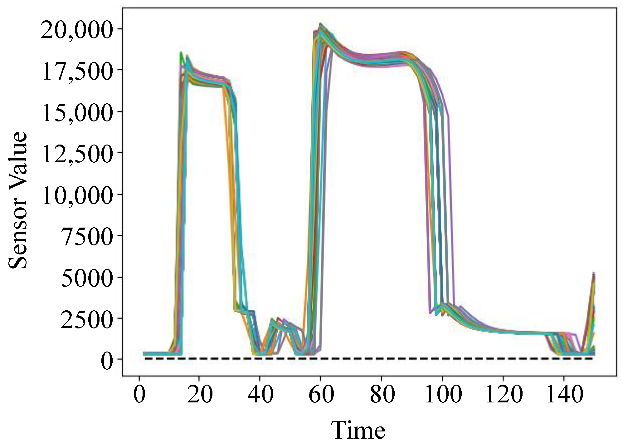
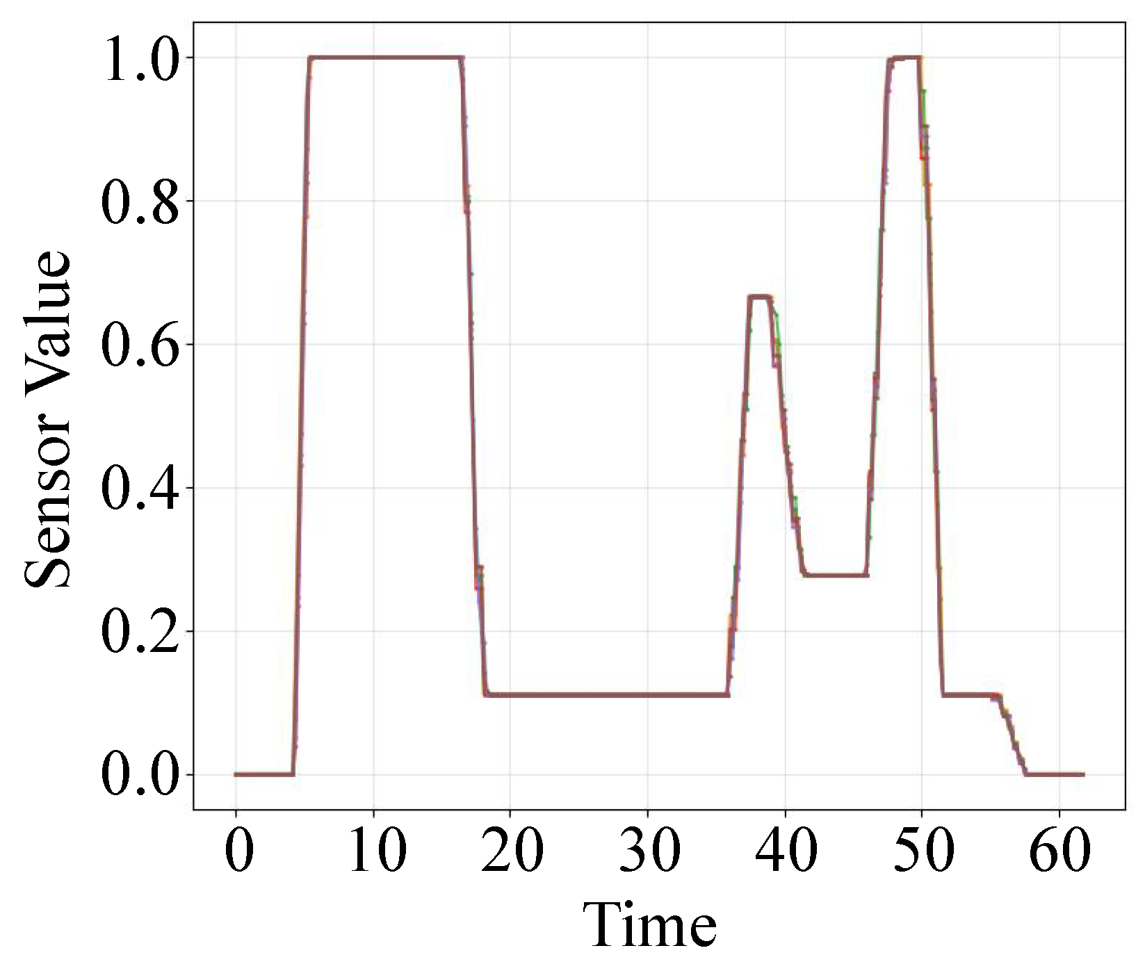
Specifically, Figure 1 depicts the value profiles of a sensor across different wafers within the same manufacturing process. From the figure, we can find the sensor readings exhibit significant inter-wafer distortions. Our objective is to identify anomalous patterns among them.
Therefore, an ideal anomaly detection framework must be architected around two components. First, it necessitates a deliberately designed alignment procedure to explicitly mitigate the distortions outlined above. Second, it requires a robust and sensitive similarity metric capable of effectively identifying anomalous patterns. We will elaborate on our proposed anomaly detection framework in Section 5.

4. Basics on Dynamic Time Warping

Dynamic Time Warping (DTW) is a classical method for comparing two temporal sequences that may share similar overall patterns but differ in their local timing or length. Intuitively, DTW finds a flexible alignment between sequences by allowing local stretching or compression of the time axis while preserving the global temporal order.
Formally, let X = ( x 1 , x 2 , , x m ) and Y = ( y 1 , y 2 , , y n ) . DTW considers a cost matrix C ( i , j ) that measures the distance between points x i and y j , and searches for a path through the matrix that minimizes the total accumulated cost:
D T W ( X , Y ) = min P ( i , j ) P C ( i , j ) ,
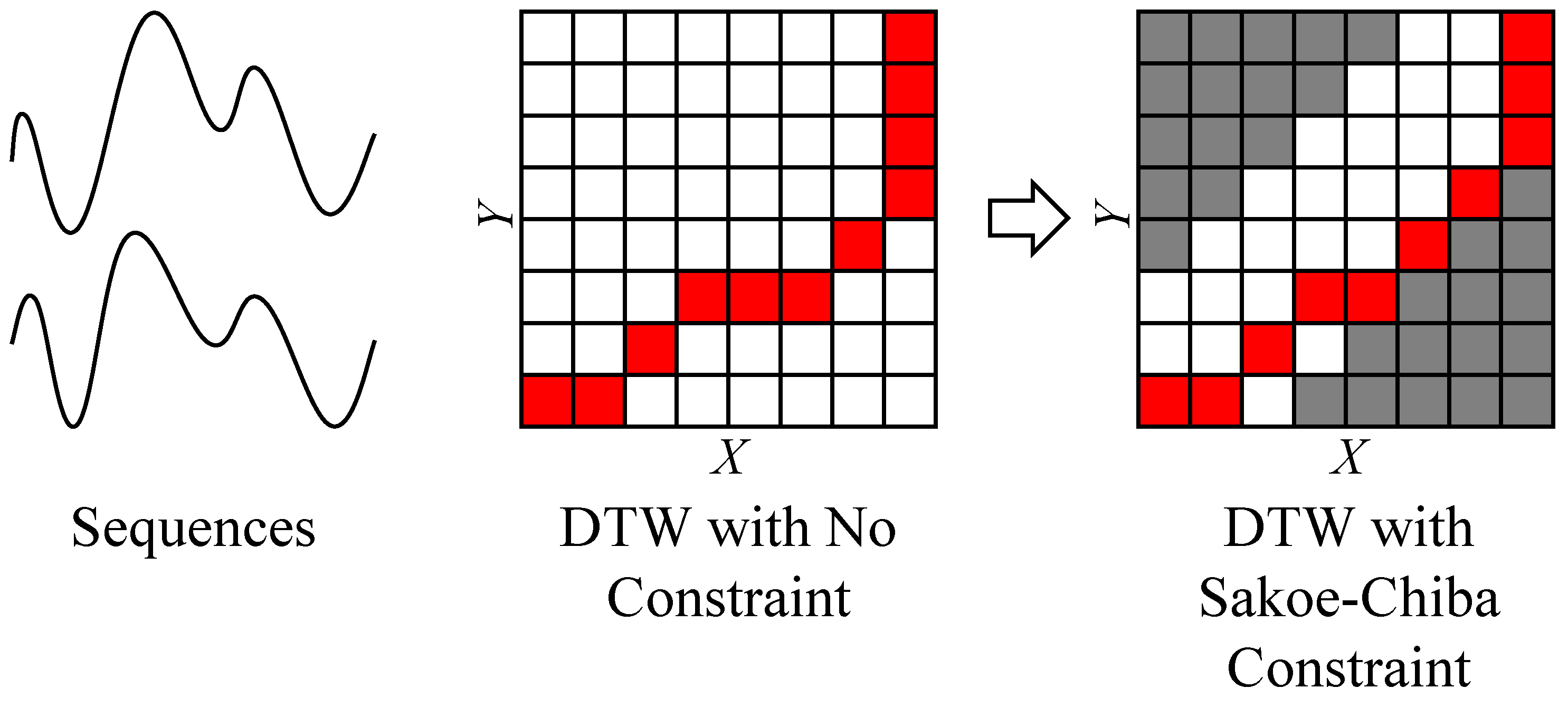
where P is a sequence of matched index pairs respecting start/end boundaries, temporal order, and allowed steps. Figure 2 (center) illustrates an example cost matrix and the optimal warping path, and the left panel shows two sequences with similar shapes but misaligned in time.

4.1. Constrained DTW

While DTW is flexible, allowing unrestricted warping may lead to unrealistic matches or high computational cost. Constrained DTW addresses this by restricting the warping path to a predefined region around the diagonal of the cost matrix, limiting how much local stretching or compression is allowed. This prevents extreme distortions and improves computational efficiency.
A common constraint is the Sakoe–Chiba band, which restricts the warping path such that each aligned pair ( i , j ) satisfies
| i j | w ,
where w is the band width that controls the maximal allowed temporal deviation from the diagonal. Figure 2 (right) illustrates a warping path constrained within such a band: the path still adapts to local timing variations but cannot deviate excessively from the diagonal.
This simple constraint not only improves efficiency by reducing the number of evaluated cells in the cost matrix but also produces more interpretable alignments by preventing very short segments from being matched to very long segments. Other types of constraint regions, such as the Itakura parallelogram, enforce similar slope-based restrictions with slightly different shapes.

4.2. Signal Alignment and DTW Average

The warping path obtained by DTW provides an explicit point-to-point correspondence between two sequences, showing which parts of one sequence match which parts of another, even if they progress at different speeds. This allows us to “align” sequences in time, effectively stretching or compressing segments to match each other.
Formally, if P is the warping path between sequences X and Y, we can define an aligned version of X with respect to Y as X ˜ , where each point in X ˜ corresponds exactly to the matched points in Y along the path P. This alignment preserves the original temporal order while compensating for local speed differences.
This idea can be naturally extended to multiple sequences { X ( k ) } k = 1 K . The goal is to compute a representative “average” sequence that captures the common pattern among all sequences. The procedure, often called the DTW average, works iteratively:
  • Initialization: Choose one sequence (or a simple pointwise average) as the initial estimate of the average sequence X ¯ .
  • Alignment: Align each sequence X ( k ) to the current average X ¯ using DTW, producing aligned sequences X ˜ ( k ) .
  • Update: Compute a new average by taking the pointwise mean of the aligned sequences:
    x ¯ j = 1 K k = 1 K x ˜ j ( k ) .
  • Iteration: Repeat the alignment and update steps until convergence.
Therefore, the DTW average can be used to capture the shared temporal patterns while ignoring local timing variations. In contrast, a naive pointwise average would blur features if sequences are misaligned in time.

5. Anomaly Detection Framework

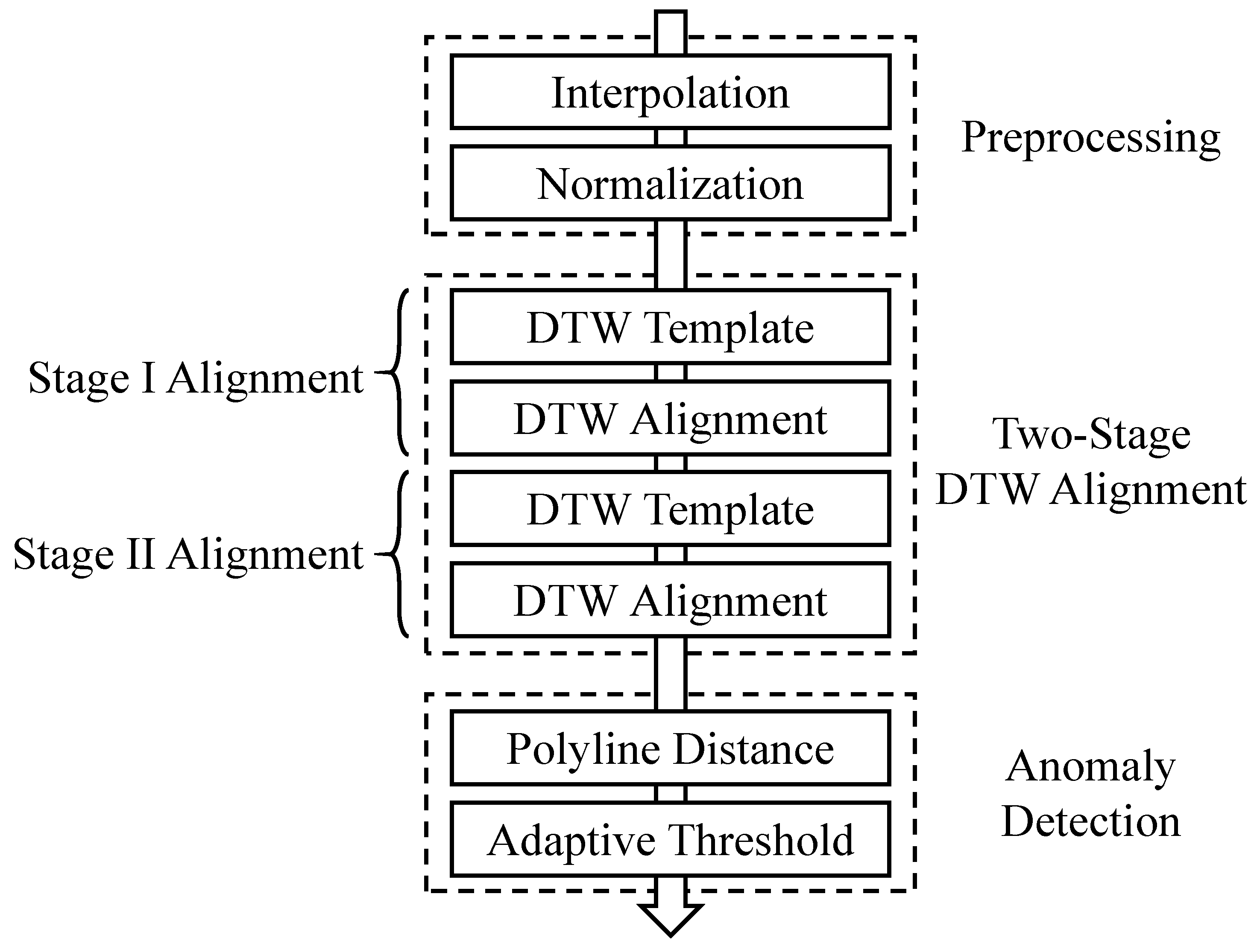
As shown in Figure 3, our proposed framework is structured into three sequential phases: Preprocessing, Two-Stage DTW Alignment, and Anomaly Detection. The initial Preprocessing process involves interpolation and normalization of the raw sensor data to mitigate inconsistencies in sampling (Section 5.1). Subsequently, the Two-Stage DTW Alignment process refines the data by constructing representative templates and performing non-linear temporal alignment to address inter-wafer variations (Section 5.2). Finally, the Anomaly Detection process employs a polyline distance metric in conjunction with an adaptive thresholding mechanism to identify anomalous patterns (Section 5.3). Each of these core components will be elaborated in detail in the subsequent sections.

5.1. Preprocessing

The preprocessing process transforms raw sensor data into a standardized format suitable for subsequent analysis. Two critical operations are performed: data interpolation and normalization.
Data Interpolation. The original sensor time series often exhibit irregular sampling intervals and varying lengths across different wafers. To address this, we apply linear interpolation to create uniform time grids. For each wafer’s sensor data, we calculate the average time step from the original process times and generate a denser temporal grid with 5× increased resolution, which is used to preserve local signal variations while avoiding excessive computational overhead. Sensor values are interpolated linearly, while step information undergoes nearest-neighbor interpolation to preserve discrete step identifiers. This process ensures all wafers share comparable temporal resolution while maintaining data integrity.
Min-Max Normalization. Sensor measurements from different wafers may exhibit varying value ranges due to systematic sensor drift and shift. We apply global Min-Max normalization to scale all sensor values to the [0,1] interval. The global minimum and maximum values are computed across all wafers’ sensor data. The transformation is defined as:
x norm = x x min x max x min
where x min and x max represent the global minimum and maximum sensor values respectively.

5.2. Two-Stage DTW Alignment

Dynamic Time Warping Barycenter Averaging (DBA) [17] is an algorithm for generating a representative time-series template from a set of sequences. It iteratively refines an initial template to capture the common morphological pattern shared across multiple input sequences, effectively minimizing the collective dynamic time warping (DTW) distance to all members in the set. This derived representative template serves as a reference for subsequent data alignment and anomaly detection tasks.
A problem is that directly applying standard DTW for alignment can lead to undesirable temporal distortions. DTW optimizes alignment by non-linearly warping the time axis to minimize point-wise Euclidean distances between sequences. A key limitation is that such unconstrained warping may excessively compress or expand certain temporal regions. For instance, a sustained anomaly spanning multiple time steps may be severely compressed during alignment, causing its amplitude or duration to be underestimated and ultimately missed by subsequent threshold-based detection methods.
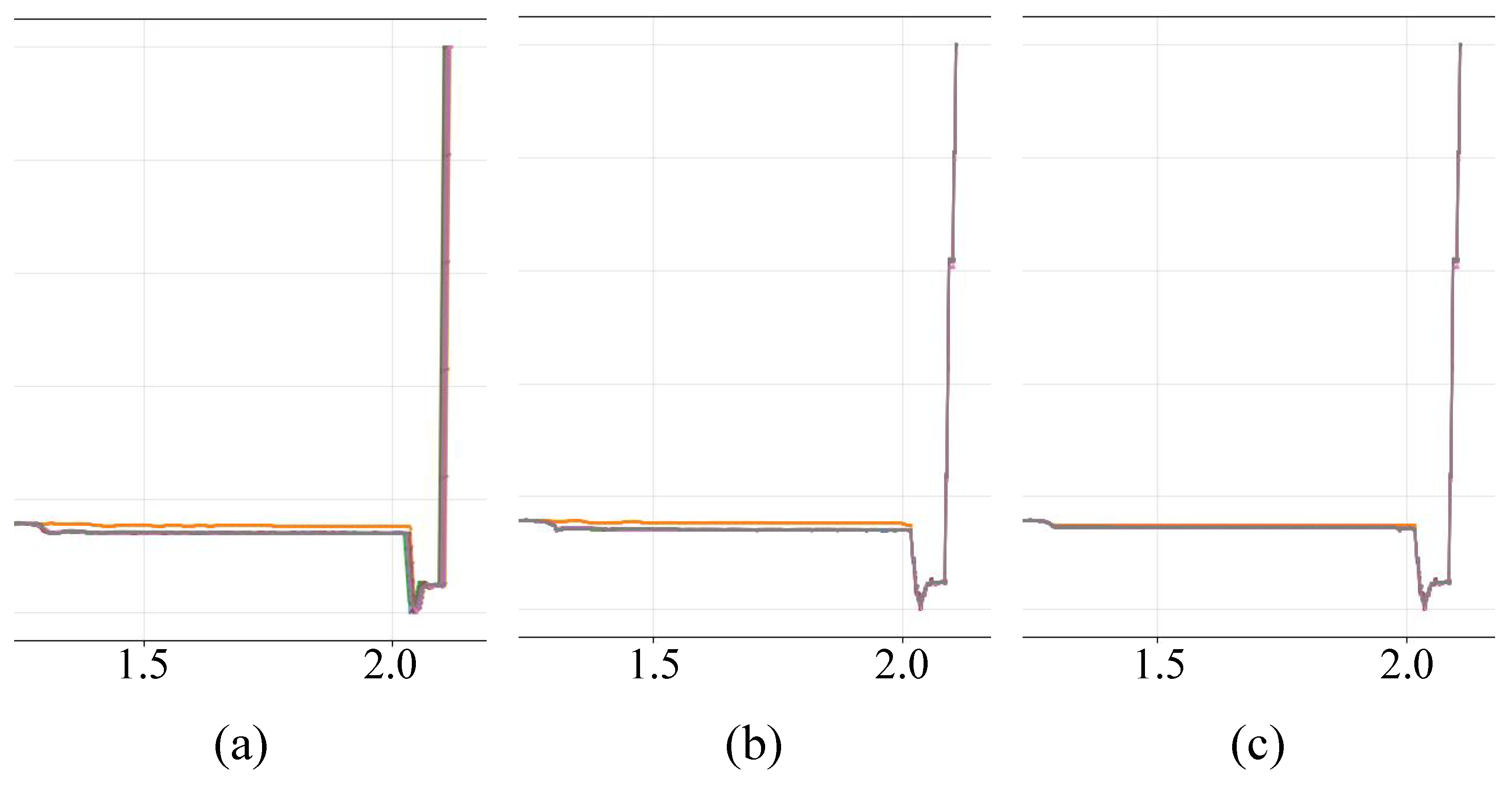
To mitigate this issue, the Sakoe–Chiba constraint [18] is introduced. This restricts the maximum allowable shift along the time axis, thereby preserving the local temporal structure and preventing extreme warping that could distort meaningful patterns. Figure 4 illustrates the effect of the Sakoe–Chiba constraint. From the figure, it can be observed that when the Sakoe–Chiba constraint is applied (Figure 4b), the original shape of the data is better preserved. In contrast, when the constraint is not used (Figure 4c), the alignment is overly permissive, which results in the failure to detect anomalies (the orange line).
The process of aligning a new data sequence to a DBA-generated template under such constraints involves the following core steps:
  • Distance Matrix Calculation: Compute the constrained DTW distance matrix between the input sequence and the reference template. This matrix encapsulates the pairwise Euclidean distances between every point in the two sequences subject to the allowed warping window.
  • Optimal Warping Path Identification: Find the optimal alignment path through the distance matrix that minimizes the cumulative distance. This path defines the non-linear mapping between the indices of the input sequence and those of the template.
  • Temporal Re-mapping: Based on the identified optimal warping path, re-map the timestamps of the input sequence to align its salient features with corresponding points in the template.
  • Interpolation and Length Normalization: Finally, apply interpolation techniques to the warped sequence to generate a uniformly sampled sequence of a standardized length, facilitating direct point-wise comparison with other aligned sequences.
However, a single DTW alignment faces inherent trade-offs: aggressive warping with large windows may overfit noise and produce unstable templates, while conservative constraints may fail to correct significant temporal shifts.
Therefore, based on the Dynamic Time Warping Barycenter Averaging algorithm, we design a two-stage alignment strategy to better handle the complex temporal distortions inherent in semiconductor manufacturing data. The key idea is to decompose the alignment process into coarse temporal correction and fine local refinement, rather than relying on a single DTW operation. Specifically, the first stage establishes coarse temporal correspondence using a relatively flexible Sakoe–Chiba window, while the second stage reconstructs an improved template and performs fine-grained alignment using a stricter window.
Let w c and w f denote the Sakoe–Chiba window sizes used in the coarse and fine alignment stages. Since the second stage is intended to correct residual misalignment after coarse alignment, we set w f w c .
Stage 1: Coarse Alignment. The initial alignment employs DTW with a constraint controlled by the coarse-stage window size w c . A reference template is computed via DBA from the normalized raw sequences. This stage is designed to accommodate substantial timing variations and correct major phase differences and rate variations, transforming disparate sequences into a more consistent temporal domain.
Stage 2: Fine Alignment. Building upon the coarsely aligned sequences, we recalculate the template and perform a second DTW alignment using a stricter constraint controlled by the fine-stage window size w f . This refined template exhibits reduced variance and better represents the common temporal pattern. The original sequences are then realigned to this improved template, enabling more precise temporal correspondence while limiting excessive local warping.
This hierarchical approach progressively improves temporal correspondence: the coarse stage handles macro temporal variations, while the fine stage addresses residual misalignments. The final aligned sequences provide a reliable foundation for subsequent anomaly detection, with temporal distortions systematically mitigated through the proposed two-stage process. The specific values of w c and w f used in the experiments are selected based on the parameter analysis in Section 6.1.

5.3. Anomaly Detection

This section presents a comprehensive anomaly detection process comprising two components: a bidirectional polyline distance metric for precise deviation quantification and an adaptive thresholding mechanism for robust decision boundaries.
Bidirectional Polyline Distance. After obtaining the time-series template via DTW-based DBA, a straightforward approach for anomaly detection is to compute the DTW distance between each wafer sequence and the template. However, this can be misleading. For instance, two sequences may have identical shapes but differ by a temporal shift. Although DBA can generate a mean template by aligning multiple sequences, the direct DTW distance between a sequence and the template may still be large. In real manufacturing data, such temporal shifts are common and should not be interpreted as anomalies.
To address this, we first “shift” each wafer sequence to minimize its DTW distance to the template, effectively compensating for temporal misalignment. This ensures that sequences with similar shapes but shifted in time are properly aligned before further distance computation.
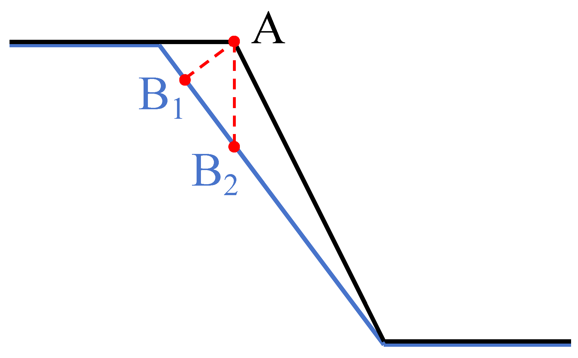
Even after DTW-based alignment, using time-based vertical distances (i.e., comparing values at corresponding time points) is still problematic. In regions with rapid changes, some points may exhibit large deviations despite overall alignment (illustrated in Figure 5, where black and blue lines are DTW-aligned sequences, but A B 2 show large residual distance).
To robustly quantify the residual geometric discrepancy, we introduce a bidirectional polyline distance. Unlike DTW or time-based distances, this metric measures the geometric distance between curves (distance A B 1 in Figure 5). For each point on the wafer sequence, we compute its shortest Euclidean distance to the template polyline, and conversely, from each template point to the wafer polyline. The local anomaly score is then defined as the maximum of these two distances:
d bidirectional = max ( d wafer template , d template wafer ) .
This bidirectional computation captures deviations from both perspectives. The point-to-polyline distance uses vector projection to find the shortest distance to line segments, with a local search restricted to temporally adjacent segments for efficiency. This geometric distance metric effectively captures both magnitude and temporal pattern deviations, providing robust and interpretable anomaly detection.
Adaptive Threshold. An adaptive thresholding strategy automatically determines anomaly detection boundaries based on the statistical distribution of bidirectional distances. The algorithm is described in Algorithm 1. We compute the global mean ( μ ) and standard deviation ( σ ) of all bidirectional distance values across all wafers. The detection threshold is defined as:
τ = μ + α · σ
where α is a sensitivity parameter controlling detection strictness. We implement a two-threshold mechanism: single-point anomalies are identified when individual distance values exceed τ , while continuous anomalies are detected when the sum of three consecutive distance values exceeds β τ where β is the continuous anomaly multiplier. In this study, both α and β are set to 2.0 by default to provide a conservative detection threshold. This setting reduces sensitivity to isolated fluctuations while still allowing continuous abnormal deviations to be detected. This ensures appropriate sensitivity to the specific statistical characteristics of the data, providing robust anomaly detection across varying process conditions.
Algorithm 1 Adaptive Anomaly Detection
Require: D: Bidirectional distance values for all wafers α : Sensitivity parameter (default: 2.0) β : Continuous anomaly multiplier (default: 2.0) τ min : Minimum threshold (default: 0.01)
Ensure: Anomaly flags for each temporal point
1:
μ mean ( D ) {Global mean of bidirectional distances}
2:
σ std ( D ) {Global standard deviation}
3:
τ max ( μ + α · σ , τ min ) {Adaptive threshold}
4:
for each wafer sequence W do
5:
    for each temporal point t in W do
6:
      if  d t > τ  then
7:
           flag [ t ] TRUE {Single-point anomaly detection}
8:
      end if
9:
      if  t 2 and i = t 2 t d i > β · τ  then
10:
           flag [ t 2 : t ] TRUE {Continuous anomaly detection}
11:
   end if
12:
  end for
13:
end for
14:
return flag

6. Case Study and Evaluation

We evaluate the performance of the proposed framework.

6.1. Parameter Selection

The Sakoe–Chiba window sizes in the two-stage DTW alignment control the flexibility of temporal warping. To examine their influence, we compare three window-size settings: ( w c , w f ) { ( 20 , 10 ) , ( 10 , 5 ) , ( 5 , 3 ) } .
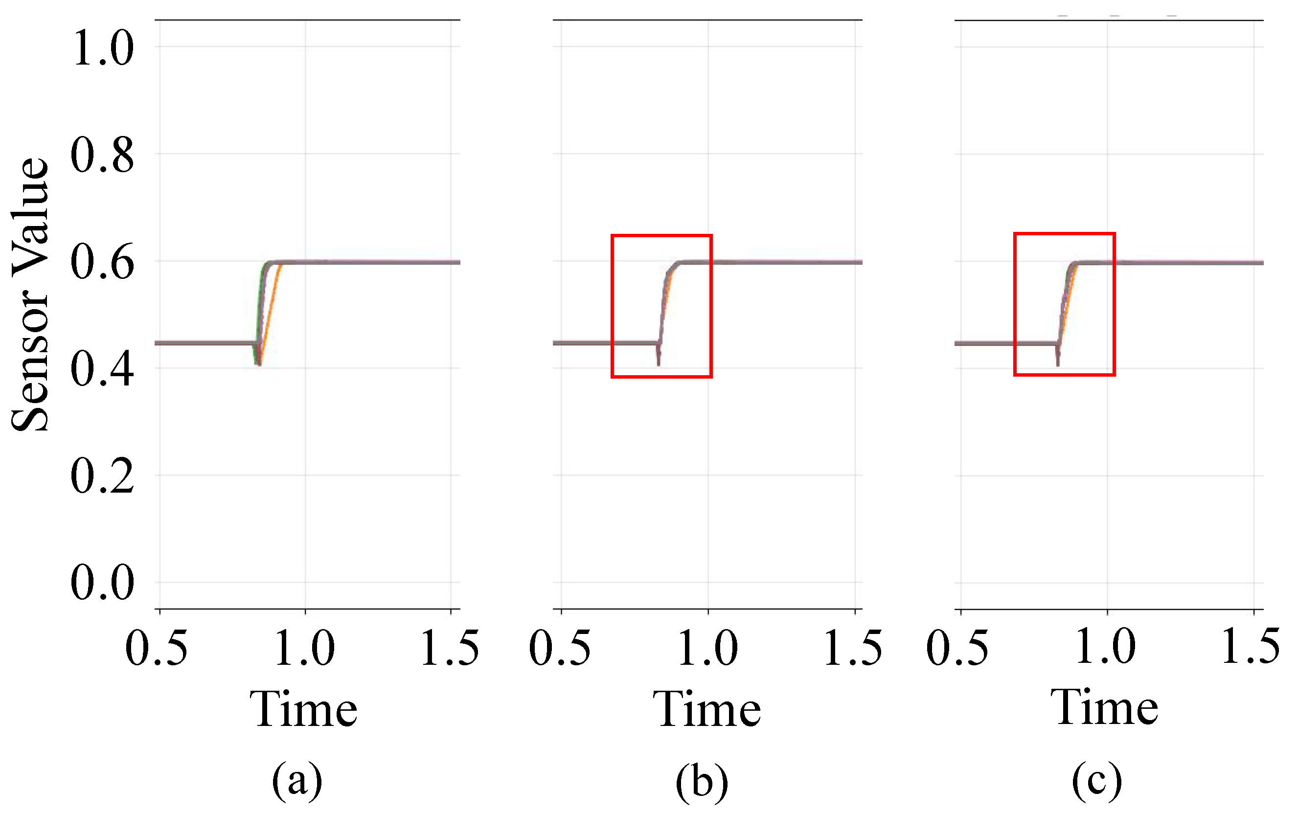
Figure 6 shows a case where the larger window setting ( 20 , 10 ) causes over-alignment. The red box highlights an abnormal region. Under ( 20 , 10 ) , the alignment is overly flexible and partially absorbs the abnormal pattern, making the anomaly less distinguishable. In contrast, ( 10 , 5 ) better preserves the local abnormal signal after alignment.
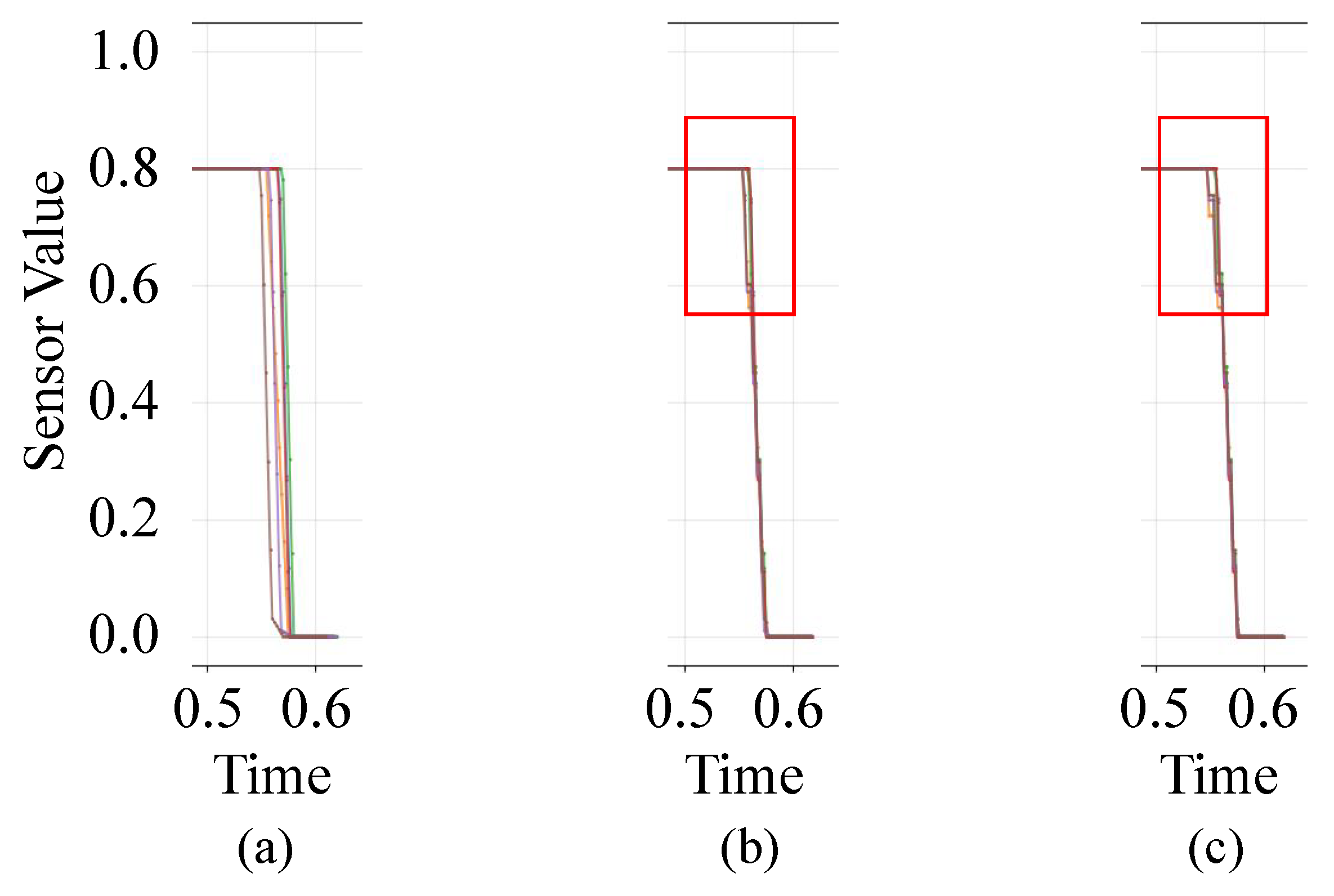
Figure 7 shows a case where the smaller window setting ( 5 , 3 ) causes under-alignment. The red box marks the region with misalignment. Under ( 5 , 3 ) , the window is too restrictive to correct the temporal shift, producing artificial differences that may lead to false positives. By comparison, ( 10 , 5 ) achieves better temporal correspondence in the highlighted region.
Based on these observations, we use ( w c , w f ) = ( 10 , 5 ) in the subsequent experiments. This setting provides a practical balance between avoiding excessive warping and correcting sufficient temporal misalignment.

6.2. Case Study I: Alignment Case

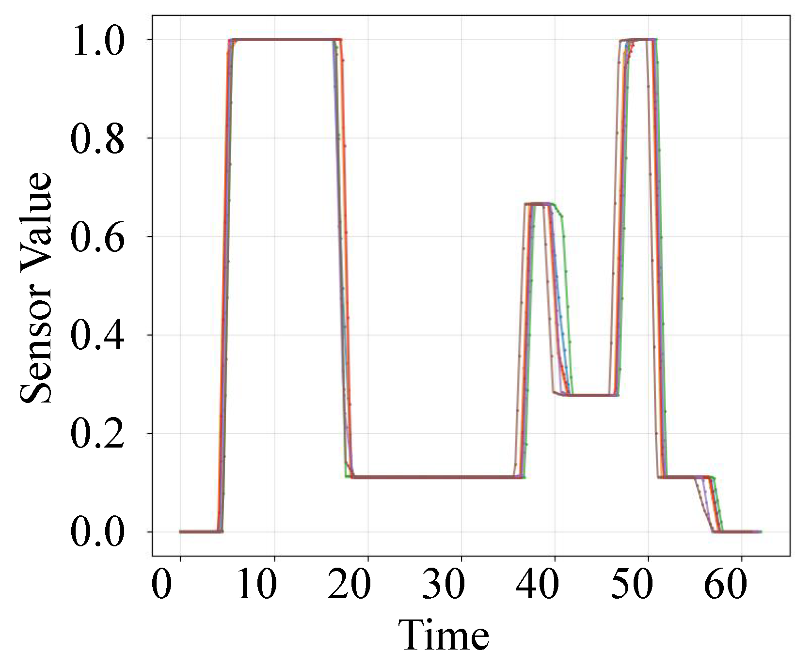
Figure 8 presents the unaligned sensor sequences from multiple wafers, exhibiting noticeable temporal shifts and morphological inconsistencies due to varying process conditions and sampling irregularities. These discrepancies complicate direct comparison and anomaly detection. In contrast, Figure 9 illustrates the results after applying our two-stage DTW alignment framework. The aligned sequences demonstrate significantly improved temporal coherence across wafers. This confirms the efficacy of the two-stage DTW strategy in mitigating inter-wafer temporal distortions.

6.3. Case Study II: Anomaly Detection Case

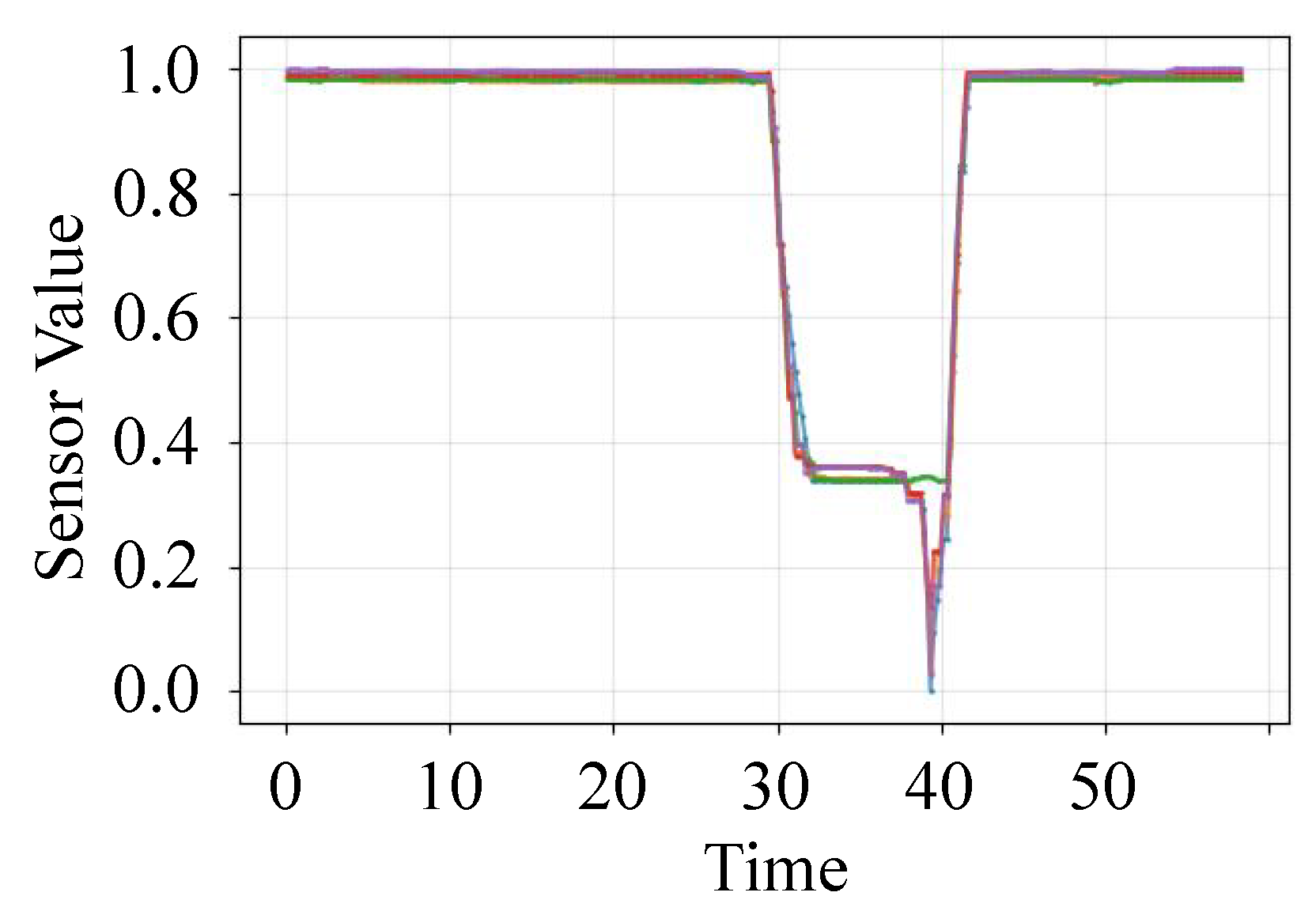
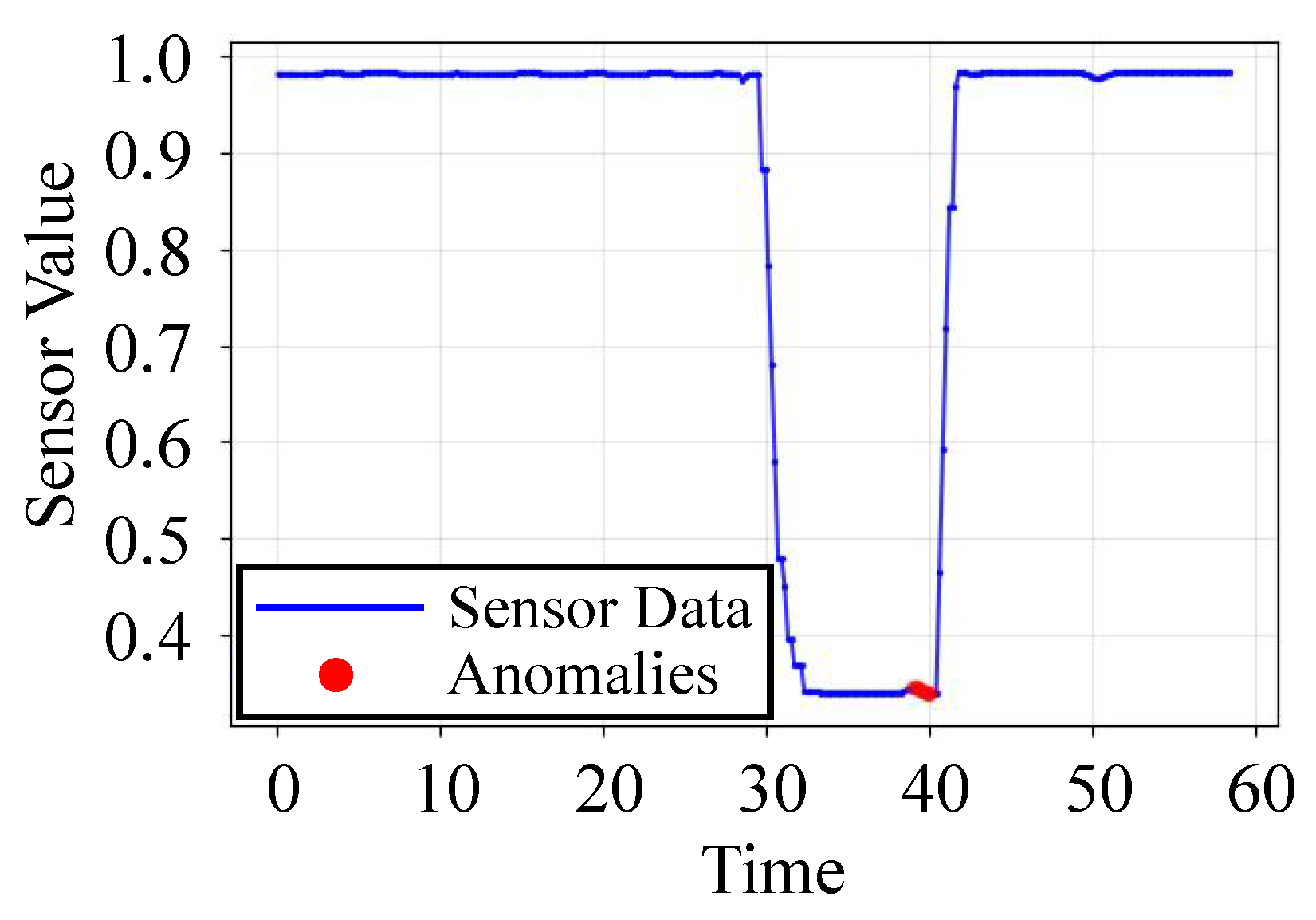
As depicted in Figure 10, the aligned sensor profiles of multiple wafers collectively form a consistent pattern, reflecting normal process behavior under stable conditions. However, a detailed examination of one specific wafer in Figure 11 reveals clear anomalous segments, highlighted in red. These regions exhibit substantial deviations from the reference template, captured effectively by our bidirectional polyline distance metric. The detected anomalies correspond to abnormal process states, which could indicate potential defects or process faults. This case demonstrates the sensitivity and discriminative capability of our anomaly detection.

6.4. Performance Evaluation

To quantify the effectiveness of the proposed framework, we conducted a comparative study against two baseline methods. The proposed method integrates constrained Dynamic Time Warping with Sakoe–Chiba constraint for alignment and the bidirectional polyline distance for anomaly detection. The two baselines are defined as follows:
  • Naive Alignment: employs standard DTW without temporal constraints for alignment, followed by the same polyline distance metric.
  • Naive Distance: uses the constrained DTW alignment as in the proposed method, but computes anomaly scores by directly comparing sensor values at the same aligned time step. Specifically, after DTW alignment, the distance is calculated as the pointwise difference between corresponding sensor values.
The selected baselines are derived from commonly used DTW-based procedures for time-series alignment and anomaly detection, and therefore provide relevant references for the scope of this study. In addition, the comparison helps show how the two-stage constrained alignment strategy and the bidirectional polyline distance improve the detection results over these basic DTW-based procedures.
The experimental evaluation is conducted on a proprietary dataset of 120 wafers, provided by Semi-Tech, a leading provider of semiconductor manufacturing software solutions. The dataset consists of multi-sensor time-series data collected directly from a semiconductor production line during a critical etching process. Specifically, the data were collected from two tools and include measurements from 17 sensors. Each data contains approximately 3000 sampling points, covering the production processes of multiple wafers. All anomaly labels were manually annotated by production line domain experts, with approximately 12% of the wafers containing identified anomalous segments.
We adopt two widely used metrics in anomaly detection: False Positive Rate (FPR) and False Negative Rate (FNR). They are defined as:
FPR = n false   positive n false   positive + n true   negative
FNR = n false   negative n false   negative + n true   positive
In semiconductor manufacturing, a low FPR is critical to avoid unnecessary process interruptions, while a low FNR ensures that defective wafers are reliably identified before moving to downstream stages.
In addition, we also report precision, recall, and F1-score to provide a more comprehensive evaluation of detection performance.
The performance comparison of the three methods is summarized in Table 2. The results demonstrate that the proposed framework achieves the lowest FPR and FNR among all methods. From the results, we observe that employing alignment without the Sakoe–Chiba constraint leads to an increase in both the FPR and FNR. This is primarily because excessive temporal warping can obscure certain anomalous patterns, thereby reducing the detection sensitivity and contributing to a higher FNR. Simultaneously, such over-alignment tends to reduce the overall variance of the aligned data, which in turn lowers the adaptive detection threshold. In some scenarios, this artificially lowered threshold can cause an increase in FPR due to the heightened sensitivity to minor fluctuations that are not truly anomalous. Furthermore, the use of point-wise absolute distance results in a substantial rise in FPR, rendering the detection system practically ineffective under realistic manufacturing conditions.

6.5. Computational Overhead

To evaluate the computational overhead of the proposed framework, we measured the runtime on a single sensor subset of the dataset used in the above experiments. This subset contains 5 wafer traces, where each wafer was monitored for approximately one minute, resulting in a total of 2936 sampling points. The reported runtime covers the full pipeline on this subset. We repeated the runtime test five times, and the measured runtime was 2.39 ± 0.11 s. These results show that the proposed framework introduces very low computational overhead. The main computational steps, including Sakoe–Chiba constrained DTW alignment and bidirectional polyline distance computation, both scale approximately linearly with the sequence length. Therefore, the runtime is expected to increase moderately with longer sequences, more sensors or more wafers. Since the current processing time is much shorter than the data acquisition duration, and the implementation can be further optimized, the method can support real-time anomaly detection in practical production-line scenarios.

7. Conclusions

This paper presents an integrated anomaly detection framework for semiconductor manufacturing through a two-stage DTW alignment strategy and a polyline distance-based detection mechanism. The coarse-to-fine alignment progressively mitigates inter-wafer temporal variations, while the bidirectional polyline distance metric with adaptive thresholding enables robust identification of anomalies. Experimental validation confirms the framework’s capability to handle real-world manufacturing data variability, providing a practical and scalable solution for wafer-level fault detection that enhances process monitoring and yield management.

Limitations and Future Work

Although the proposed framework has been validated on real semiconductor production-line data, the current evaluation is still limited by the scale and availability of proprietary industrial data. As a result, the generalizability of the findings may be limited. In addition, the experimental comparison is limited to DTW-based baselines, and broader comparisons with other anomaly detection methods remain to be further explored. In future work, we will further test the method in production-line deployments and explore anonymized benchmark datasets for broader reproducibility.

Author Contributions

Conceptualization, G.L. and Z.Y. (Zhice Yang); methodology, G.L., Y.H., Z.Y. (Zaizhou Yang) and Z.Y. (Zhice Yang); software, G.L., Y.H. and Z.Y. (Zaizhou Yang); validation, G.L., Y.H., Z.Y. (Zaizhou Yang) and Z.Y. (Zhice Yang); formal analysis, G.L. and Y.H.; investigation, Y.H.; resources, G.L.; data curation, G.L.; writing—original draft preparation, G.L. and Y.H.; writing—review and editing, Z.Y. (Zhice Yang); visualization, G.L. and Y.H.; supervision, Z.Y. (Zhice Yang); project administration, G.L. All authors have read and agreed to the published version of the manuscript.

Funding

This research received no external funding.

Institutional Review Board Statement

Not applicable.

Informed Consent Statement

Not applicable.

Data Availability Statement

The data used in this study are proprietary semiconductor manufacturing data and are not publicly available.

Acknowledgments

During the preparation of this manuscript, the authors used GPT-5.4 and DeepSeek-V3.2 for the purposes of translation, text polishing, and coding assistance. The authors have reviewed and edited the output and take full responsibility for the content of this publication.

Conflicts of Interest

This work was supported by Semi-Tech. Gangjiang Li serves as Chairman of Semi-Tech. The remaining authors declare no conflicts of interest.

Abbreviations

The following abbreviations are used in this manuscript:
DTWDynamic Time Warping
FDCFault Detection and Classification
DBADynamic Time Warping Barycenter Averaging
FPRFalse Positive Rate
FNRFalse Negative Rate

References

  1. Chen, H.-Y.; Chen, C. Reviews of the Static, Adoptive, and Dynamic Sampling in Wafer Manufacturing. Appl. Syst. Innov. 2025, 9, 1. [Google Scholar] [CrossRef] [Scilit]
  2. Yeo, W.; Chang, Y.C.; Chen, L.C.; Chang, K.H. A Novel Out-of-Control Action Plan (OCAP) for Optimizing Efficiency and Quality in the Wafer Probing Process for Semiconductor Manufacturing. Sensors 2024, 24, 5116. [Google Scholar] [CrossRef] [Scilit] [PubMed]
  3. Gang, D.; He, Y.; Shao, X. Anomaly Detection and Analysis of FDC Data. In Proceedings of the 2021 5th IEEE Electron Devices Technology & Manufacturing Conference (EDTM); IEEE: New York, NY, USA, 2021; pp. 1–3. [Google Scholar] [CrossRef] [Scilit]
  4. Owens, R.; Sun, F.K.; Venditti, C.; Blake, D.; Dillon, J.; Boning, D. Dynamic Time Warping Constraints for Semiconductor Processing. In Proceedings of the 2024 35th Annual SEMI Advanced Semiconductor Manufacturing Conference (ASMC); IEEE: New York, NY, USA; pp. 1–6. [CrossRef] [Scilit]
  5. Chien, C.F.; Wang, W.C.; Cheng, J.C. Data mining for yield enhancement in semiconductor manufacturing and an empirical study. Expert Syst. Appl. 2007, 33, 192–198. [Google Scholar] [CrossRef] [Scilit]
  6. Khakifirooz, M.; Chien, C.F.; Chen, Y.J. Bayesian inference for mining semiconductor manufacturing big data for yield enhancement and smart production to empower industry 4.0. Appl. Soft Comput. 2018, 68, 990–999. [Google Scholar] [CrossRef] [Scilit]
  7. Lee, K.B.; Cheon, S.; Kim, C.O. A Convolutional Neural Network for Fault Classification and Diagnosis in Semiconductor Manufacturing Processes. IEEE Trans. Semicond. Manuf. 2017, 30, 135–142. [Google Scholar] [CrossRef] [Scilit]
  8. Kim, E.; Cho, S.; Lee, B.; Cho, M. Fault Detection and Diagnosis Using Self-Attentive Convolutional Neural Networks for Variable-Length Sensor Data in Semiconductor Manufacturing. IEEE Trans. Semicond. Manuf. 2019, 32, 302–309. [Google Scholar] [CrossRef] [Scilit]
  9. Lee, S.; Choi, J.; Kim, M.S. Generative pre-training of time-series data for unsupervised fault detection in semiconductor manufacturing. arXiv 2023, arXiv:2309.11427. [Google Scholar]
  10. Chen, C.Y.; Chang, S.C.; Liao, D.Y. Equipment anomaly detection for semiconductor manufacturing by exploiting unsupervised learning from sensory data. Sensors 2020, 20, 5650. [Google Scholar] [CrossRef] [Scilit] [PubMed]
  11. Hsu, C.Y.; Liu, W.C. Multiple time-series convolutional neural network for fault detection and diagnosis and empirical study in semiconductor manufacturing. J. Intell. Manuf. 2021, 32, 823–836. [Google Scholar] [CrossRef] [Scilit]
  12. Hwang, R.; Park, S.; Bin, Y.; Hwang, H.J. Anomaly detection in time series data and its application to semiconductor manufacturing. IEEE Access 2023, 11, 130483–130490. [Google Scholar] [CrossRef] [Scilit]
  13. Kim, Y.; Lee, H.; Kim, C.O. A variational autoencoder for a semiconductor fault detection model robust to process drift due to incomplete maintenance. J. Intell. Manuf. 2023, 34, 529–540. [Google Scholar] [CrossRef] [Scilit]
  14. Liu, Y.; Wang, W.; Wu, Y. Titad: Time-invariant transformer for multivariate time series anomaly detection. Electronics 2025, 14, 1401. [Google Scholar] [CrossRef] [Scilit]
  15. Shyalika, C.; Roy, K.; Prasad, R.; Kalach, F.E.; Zi, Y.; Mittal, P.; Narayanan, V.; Harik, R.; Sheth, A. RI2AP: Robust and interpretable 2D anomaly prediction in assembly pipelines. Sensors 2024, 24, 3244. [Google Scholar] [CrossRef] [Scilit] [PubMed]
  16. Cools, A.; Belarbi, M.A.; Mahmoudi, S.A. Benchmarking of anomaly detection methods for industry 4.0: Evaluation, ranking, and practical recommendations. Big Data Cogn. Comput. 2025, 9, 128. [Google Scholar] [CrossRef] [Scilit]
  17. Petitjean, F.; Ketterlin, A.; Gançarski, P. A global averaging method for dynamic time warping, with applications to clustering. Pattern Recognit. 2011, 44, 678–693. [Google Scholar] [CrossRef] [Scilit]
  18. Sakoe, H.; Chiba, S. Dynamic programming algorithm optimization for spoken word recognition. IEEE Trans. Acoust. Speech Signal Process. 2003, 26, 43–49. [Google Scholar] [CrossRef] [Scilit]
Figure 1. Time Series in Semiconductor Manufacturing. The value profiles of a sensor across different wafers within the same manufacturing process. Different colored lines represent sensor traces from different wafers.
Applsci 16 05779 g001
Figure 2. An example of DTW with Sakoe–Chiba constraint. Red cells denote the optimal warping path, gray cells denote excluded regions, and white cells denote feasible regions.
Applsci 16 05779 g002
Figure 3. Overview of the DTW-based multi-stage alignment and anomaly detection framework.
Applsci 16 05779 g003
Figure 4. Alignment with Sakoe–Chiba constraint vs. w/o Sakoe–Chiba constraint. (a) Before Alignment; (b) Align with Sakoe–Chiba Constraint; (c) Align without Sakoe–Chiba Constraint. Different colored lines represent sensor traces from different wafers.
Applsci 16 05779 g004
Figure 5. Distance between polyline distance ( A B 1 ) and time-based distance ( A B 2 ).
Applsci 16 05779 g005
Figure 6. Over-alignment case under a large window setting. (a) Sequences before alignment; (b) Alignment with ( w c , w f ) = ( 20 , 10 ) ; (c) Alignment with the proposed setting ( 10 , 5 ) . The red box highlights an abnormal region that is overly warped and becomes less distinguishable under ( 20 , 10 ) , while it is better preserved under ( 10 , 5 ) . Different colored lines represent sensor traces from different wafers.
Applsci 16 05779 g006
Figure 7. Under-alignment case under a small window setting. (a) Sequences before alignment; (b) Alignment with ( w c , w f ) = ( 5 , 3 ) ; (c) Alignment with the proposed setting ( 10 , 5 ) . The red box marks a region with residual misalignment under ( 5 , 3 ) , which is better corrected by the proposed setting ( 10 , 5 ) . Different colored lines represent sensor traces from different wafers.
Applsci 16 05779 g007
Figure 8. Sensor values before two-stage DTW alignment. Different colored curves represent sensor traces of different wafers, which show temporal shifts before alignment.
Applsci 16 05779 g008
Figure 9. Sensor values after two-stage DTW alignment. Different colored curves represent sensor traces of different wafers. The aligned curves exhibit improved temporal consistency.
Applsci 16 05779 g009
Figure 10. Aligned sensor data for anomaly detection. Different colored lines denote the sensor data of different wafers.
Applsci 16 05779 g010
Figure 11. Detected Anomalies. The time-series sensor data is the green line in Figure 10.
Applsci 16 05779 g011
Table 1. Example of one observation record.
TimeWafer_IDStepNumberSensor_1Sensor_2Sensor_3Sensor_4
100WAFER_A0110.00100.02340
Table 2. Performance evaluation results.
MethodFPR (%)FNR (%)PrecisionRecallF1-Score
Naive Alignment23.3646.150.220.540.31
Naive Distance38.3230.770.180.690.29
Ours6.5430.770.560.690.62
Note: Bold values indicate the best performance for each metric, with ties also shown in bold.
Disclaimer/Publisher’s Note: The statements, opinions and data contained in all publications are solely those of the individual author(s) and contributor(s) and not of MDPI and/or the editor(s). MDPI and/or the editor(s) disclaim responsibility for any injury to people or property resulting from any ideas, methods, instructions or products referred to in the content.