Article

Development of Ultra-Fast Surface Acoustic Wave-Based NO2 Sensor Incorporating a Monolayered Graphene: MoS2 Sensing Material and a Microheater for Spacecraft Applications

by
Faisal Nawaz
1,
Hyunho Lee
2,
Wen Wang
3 and
Keekeun Lee
1,2,*
1
Department of Electrical and Computer Engineering, Ajou University, Suwon 16499, Republic of Korea
2
Department of Intelligence Semiconductor Engineering, Ajou University, Suwon 16499, Republic of Korea
3
Institute of Acoustic, Chinese Academy of Sciences, Beijing 100190, China
*
Author to whom correspondence should be addressed.
Appl. Sci. 2025, 15(7), 4050; https://doi.org/10.3390/app15074050
Submission received: 22 February 2025 / Revised: 30 March 2025 / Accepted: 31 March 2025 / Published: 7 April 2025
(This article belongs to the Section Surface Sciences and Technology)

Abstract

:
A surface acoustic wave-based NO2 sensor and its interface electronics, utilizing monolayered two-dimensional sensing materials, were developed for internal pollution monitoring in spacecraft. The sensor system consists of a two-port SAW delay line with monolayered graphene/MoS2 flakes in the cavity region between two interdigital transducers, along with the interface electronics. A microheater was integrated adjacent to the sensor to maintain a stable temperature field on the sensor surface, thereby enhancing sensitivity, response/recovery times, and selectivity. The monolayered graphene/MoS2 sensing material, with its high surface-to-volume ratio, excellent mobility, and moderate bonding force with target molecules, enables the rapid response and recovery times of less than 2.5 and 8 s, respectively—among the fastest reported in SAW gas sensor technology. The developed sensor combines the conductivity changes, the mass loading effect, and a synergistic effect that promotes carrier separation caused by a built-in potential barrier between the two monolayers, providing exceptionally high sensitivity of 578 Hz/ppm. Additionally, the sensor’s interface electronics were engineered to mitigate the effects of external factors, such as temperature and humidity, ensuring a stable and reliable performance under varying harsh conditions.

1. Introduction

The number of astronauts who stay inside a confined spacecraft for several months or years while carrying out missions is increasing. Despite the presence of air purification systems, it is known that air pollution inside the spacecraft is 2 to 5 times higher than in enclosed environments with a terrestrial atmosphere [1]. According to NASA’s manned lunar exploration program, the Artemis mission, astronauts have reported that they may suffer from severe odors caused by bathroom waste throughout the duration of the mission [2]. The main sources of polluted gases inside the spacecraft include gas production from heat and friction during equipment manipulation, degassing from internal materials over time, leaks from gas pipelines, and gases generated by astronauts’ physical activity, metabolism, and waste during their stay [3,4]. According to NASA’s Spacecraft Maximum Allowable Concentrations (SMAC) list, over 300 gases have been reported inside spacecraft. Of these, 21 are classified as hazardous [5]. Table 1 presents the main hazardous gases and their respective allowable concentration limits within the spacecraft. Among them, NO2 is particularly toxic and dangerous [6,7,8,9,10]. It is acidic, highly reactive, has an unpleasant odor, and is continuously produced and released into the atmosphere as a result of human activities. Even at low concentrations (~1 ppm), NO2 can cause serious damage to the respiratory system and lung tissues. It can also lead to diseases, such as emphysema and bronchitis, while exacerbating existing heart conditions. Given its toxicity and hazards, there is an urgent need for the accurate and rapid detection of low NO2 levels in the environment.
Several NO2 sensing materials have been reported, including graphene, transition metal dichalcogenides (TMDs), metal oxide nanostructures, and others [11,12]. Among these, single-layer two-dimensional (2D) materials exhibit the most ideal characteristics for NO2 sensing [13,14,15]. Two-dimensional materials, such as graphene and MoS2, exhibit a high surface-to-volume ratio, high mobility, and moderate bonding with target molecules, leading to fast response and recovery times. MoS2 exists in two possible crystal phases, trigonal and hexagonal. The hexagonal phase is semiconducting, while the trigonal phase exhibits metallic properties. In its bulk semiconducting (hexagonal) phase, MoS2 has an indirect bandgap of 1.2 eV. However, when reduced to a monolayer, MoS2 transitions to a direct bandgap of 1.8 eV [16,17,18]. The weak van der Waals forces between the layers in the bulk form facilitate the easy exfoliation and transfer of the material. Additionally, ideal MoS2 is known to be free of dangling bonds. However, at defect sites (such as vacancies, dopants, adsorbates, adatoms, and impurities) and along the edges of the 2D material, strong bonding interactions occur, enhancing its reactivity with gas molecules [19,20,21,22]. Furthermore, MoS2 can exhibit either n-type or p-type behavior, depending on the perturbations caused by defects. Graphene, another 2D material, has a zero bandgap [23,24]. Similar to MoS2, its electronic properties can be modified by defects, which can result in the formation of strong bonds with target molecules. Although 2D NO2 sensing materials with high performance have been reported in the literature, several challenges remain [25,26].
This study focuses on the development of an NO2 sensor for spacecraft applications. In such environments, the sensor must meet several key requirements, including proper operation in oxygen-free and zero-gravity conditions, high sensitivity, fast response/recovery times, no degassing from the sensor itself, effective compensation for temperature and humidity, and UV-C radiation. The key innovations and advantages of the developed surface acoustic wave (SAW)-based NO2 sensor system are as follows: For the first time, a monolayer 2D sensing material has been integrated into SAW technology to create an NO2 sensor. Our SAW sensor platform eliminates the need for direct current or voltage applied to the sensing material, thereby preventing Joule heating, atomic evaporation from the surface, and degassing from the sensor itself. The sensor demonstrates exceptionally rapid response and recovery times by utilizing a monolayer graphene/MoS2 heterostructure within SAW technology. Most importantly, it operates effectively in both oxygen-free and zero-gravity environments, thanks to the use of the 2D sensing materials. The sensor capitalizes on both conductivity changes and mass loading, resulting in exceptionally high sensitivity. Additionally, the sensor’s interface electronics incorporates a built-in compensation feature that mitigates the effects of external perturbation factors, such as temperature, humidity, and UV-C radiation, ensuring stable performance under varying conditions.

2. Optimal Design Consideration and Analytical Modeling

2.1. Operating Mechanism

Figure 1 shows the overall schematic of the developed SAW-based NO2 sensor and interface electronics. The system consists of two SAW devices with identical structure and performance, two oscillators, a mixer, a low-pass filter (LPF), a comparator, a field-programmable gate array (FPGA), and a PC. A microheater and temperature sensor are integrated around the sensor to maintain a stable temperature field. A two-port SAW delay line is formed on a 128° YX LiNbO3 substrate. The reason for employing the two-port SAW delay line is to provide a larger sensing area between the two interdigital transducers (IDTs). The NO2 sensing material (2D graphene/MoS2) is applied to the cavity region between the two IDTs.
The adsorption of NO2 molecules on the sensing material increases the hole concentration in the p-type MoS2, leading to an increase in conductivity. Similarly, NO2 molecules, acting as electron acceptors, enhance the conductivity of the p-type graphene sensing material. A built-in potential barrier is formed between the two monolayers due to the potential energy (P.E.) difference between the two materials, which creates a synergistic effect that promotes carrier separation without the immediate recombination of carriers. Specifically, electrons are transferred from MoS2 to graphene, and holes are transferred from graphene to MoS2, minimizing recombination and enhancing charge conductivity. The bonding between the two monolayers is Van der Waals bonding.
Furthermore, the adsorption of NO2 molecules induces mass loading on the sensing material, which reduces the propagation velocity of surface acoustic waves. This results in an amplified change in amplitude and a frequency downshift at the output IDT. By calibrating the frequency change with NO2 concentration, the sensor provides measurable output information.

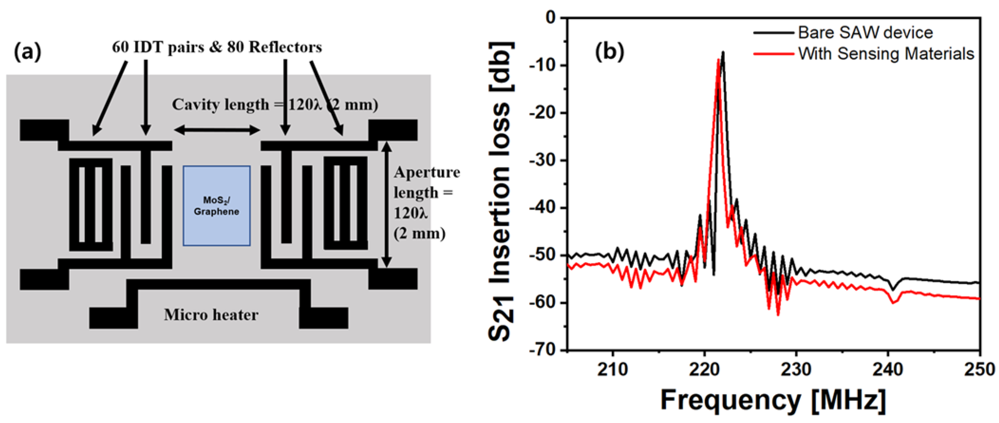
2.2. COM Modeling of the SAW Sensor Platform

A two-port SAW delay line with a center frequency of 222 MHz was designed on a 128° YX LiNbO3 piezoelectric substrate using coupling of mode (COM) modeling. The SAW-based sensor platform involves several parameters, including substrate, center frequency, IDT pair, aperture length, metal selection, metal thickness, cavity length, and so on. By modulating these parameters, the optimal design specifications are derived. Figure 2 shows the S21 scattering parameter as a function of frequency, obtained using the optimized parameters listed in Table 2. The S21 characteristics show low insertion loss at the center frequency of 222 MHz, high side lobes, and minimal parasitic conduction at high frequencies. The sensing material is applied to the cavity region between the two IDTs. No significant change in the central frequency was observed due to the minimal mass loading of the monolayer sensing material. Based on this, the sensor was fabricated, and the experimental results closely matched the analytical modeling predictions. The detailed process of COM modeling has been thoroughly explained in our previous research [27,28,29]; therefore, this study omits that explanation.

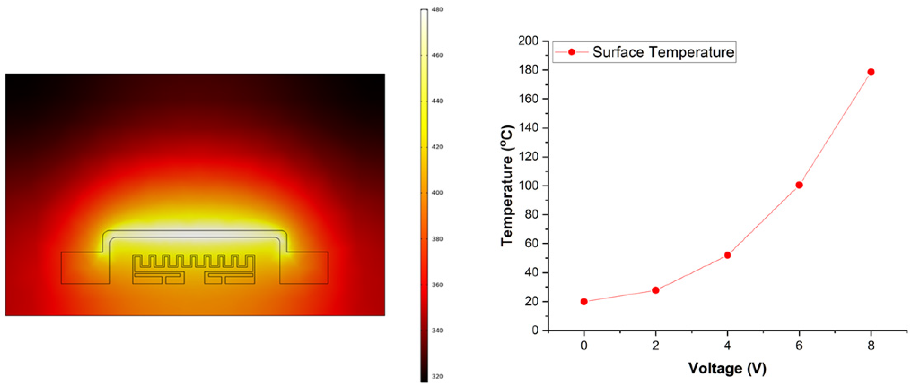
2.3. COMSOL Simulation of the Microheater

A microheater was integrated adjacent to the sensor to maintain a stable surface temperature, thereby enhancing the sensor’s sensitivity, response/recovery time, and selectivity. The operating principle of the microheater is that, when a voltage is applied, an electric field is generated inside the conductor. This electric field accelerates the electrons, which then collide with the lattice. The energy from these collisions is converted into thermal energy, proportional to the intensity of the electric field. As a result, heat is generated within the conductor, and simultaneously, the heat is transferred to the surrounding medium through thermal conduction, thermal radiation, and thermal convection. The maintenance of a stable temperature is not solely due to radiative heat loss but rather a balance between all heat transfer mechanisms, including conduction, convection, and radiation. In our system, the thermal energy generated by electron–lattice collisions reaches equilibrium with the heat dissipated through conduction (to the substrate and surrounding structures), convection (to the surrounding air), and radiation (to the environment). This balance ensures an almost stable temperature filed during operation.
Using the COMSOL simulator (V6.3), a microheater was designed on a 128° YX LiNbO3 substrate. The structural parameters of the microheater include the material, length, thickness, and width. By optimizing these parameters, the microheater’s specifications were derived for optimal performance. Its placement and orientation were carefully designed to maximize heat transfer efficiency to the sensing area, ensuring stable and uniform thermal distribution (Figure 3). COMSOL thermal simulations served two primary purposes: (1) the modeling and visualizing the propagation of heat toward the cavity region (sensing area) under microheater activation, and (2) optimizing the heater design (e.g., length, width, placement) to maximize heat delivery efficiency. The temperature distribution demonstrates effective heat localization, achieving the necessary thermal conditions for enhanced sensor performance. Platinum (Pt) was selected as the material for the microheater due to its stable properties, even at very high temperatures over extended periods. Platinum (Pt) generally has a high melting point of 1768 °C. At driving temperatures below 90 °C, Pt degassing due to Joule heating is expected to be minimal. The microheater dimensions are 2 mm in length, 100 nm in thickness, and 500 µm in width. The temperature sensor, located directly below the microheater in the same position as the sensing area, has dimensions of 1.5 mm in length, 100 nm in thickness, and 500 µm in width. The heater exhibits a resistance of 50 ohms at room temperature. A DC voltage was applied to the designed microheater (Figure 3), leading to a temperature increase around the cavity of the SAW sensor. In our simulation setup, applied voltage was set to 5 V, the temperature in the cavity region was estimated to be approximately 90 °C based on the designed structure. Additionally, it was confirmed that the microheater exhibited excellent response time, recovery time, long-term stability, and repeatability.

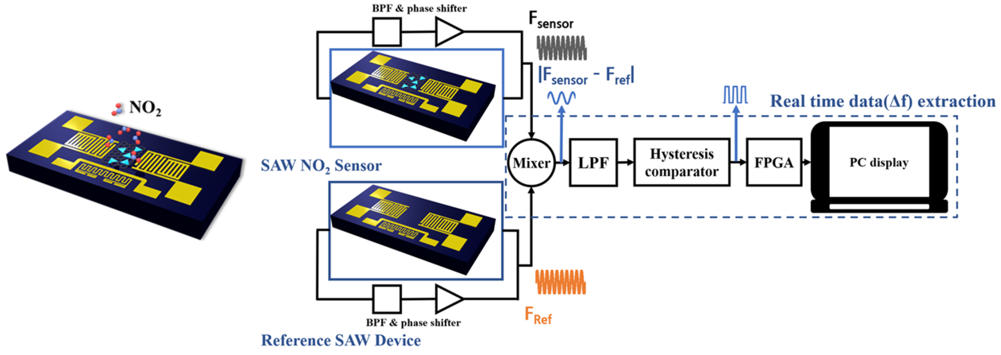
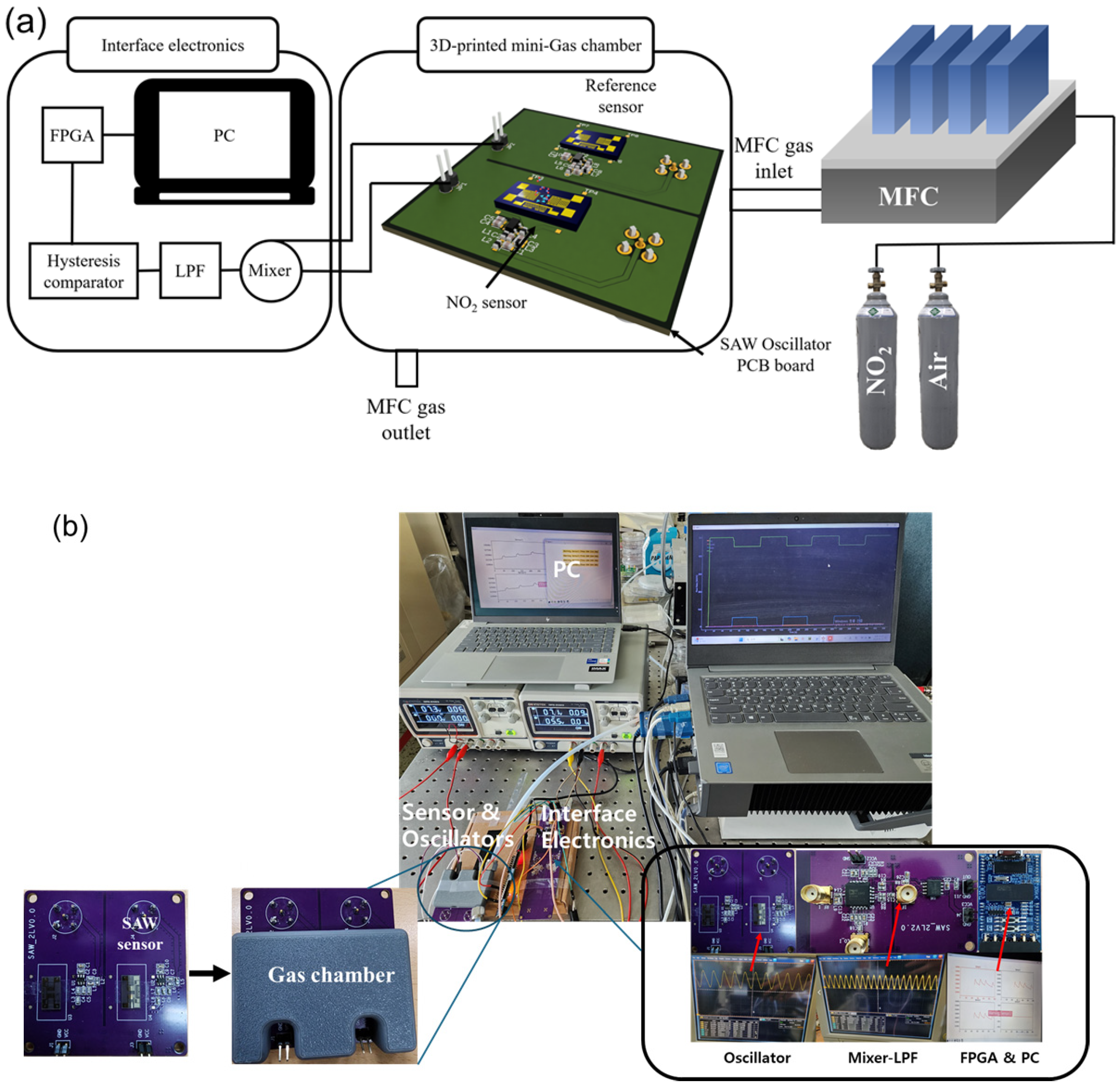
3. Experimental Methods

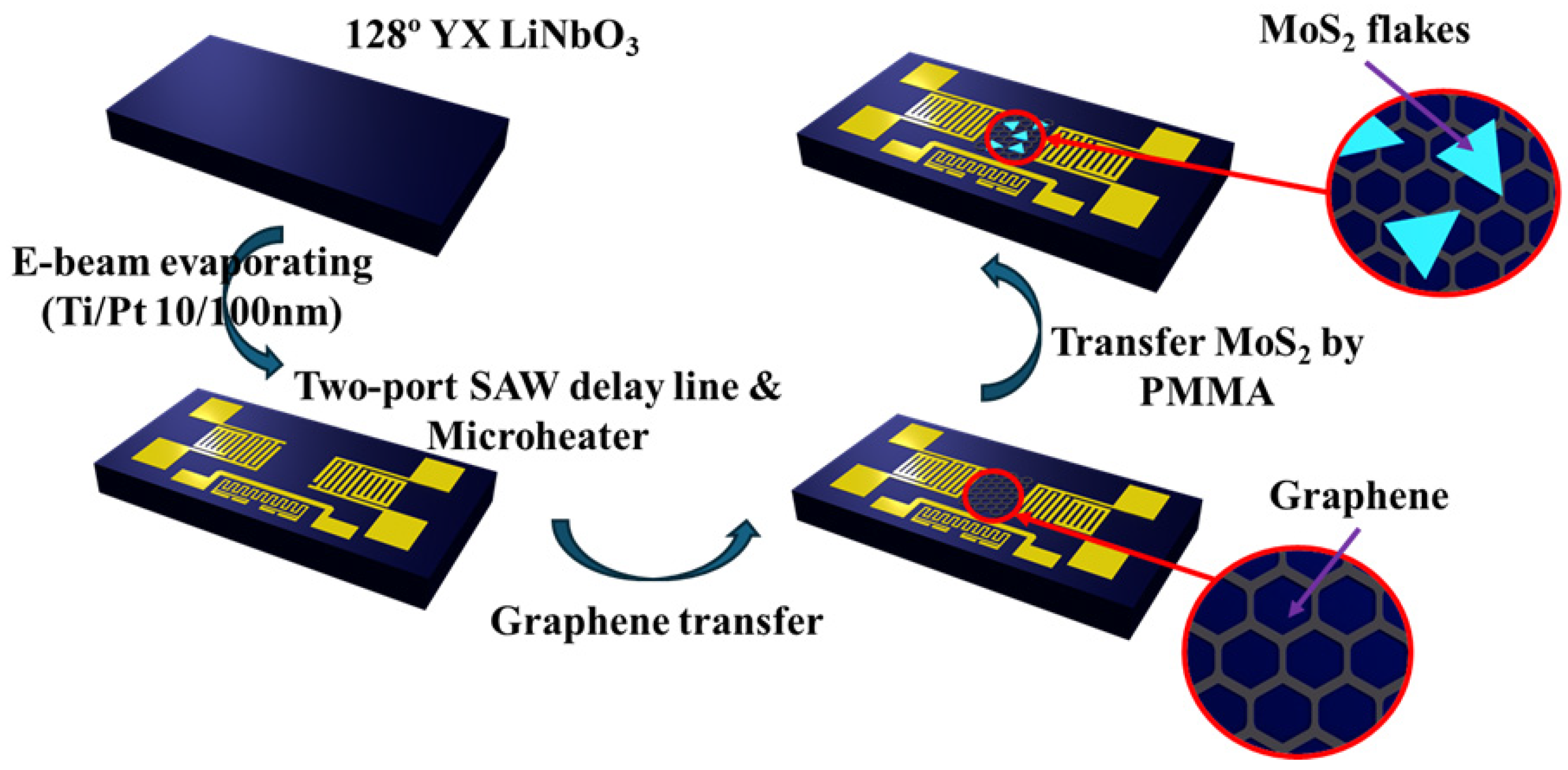
3.1. SAW Sensor Platform Fabrication

Figure 4 shows the fabrication process of the two-port SAW delay line and microheater. A 4-inch 128° YX LiNbO3 substrate was cleaned in sequence with Acetone, IPA, and DI Water to remove organic materials and residues from the surface. The DNR-L300 negative photoresist (PR) was then spin-coated onto the wafer, with coating speeds of 500/4000/500 rpm to form a thickness of approximately 3 μm, followed by a soft bake at 90 °C for 90 s on a hot plate. UV exposure was carried out using a chrome mask, with a UV power of 13.4 mW for approximately 15 s. After exposure, a hard bake was performed at 110 °C for 90 s to enhance the stability of the PR. Finally, the exposed patterns were developed by immersing the wafer in Developer AZ 300 MIF solution for 30 s. The PR-patterned wafer was then subjected to Ti/Pt deposition (10/100 nm thickness) using an E-beam evaporator, followed by a lift-off process to complete the two-port SAW delay line and the microheater. A dicing saw was used to separate the wafer into individual devices.

3.2. Sensing Material Fabrication

Two different sensing materials were fabricated. The first sensor is a heterostructure combining graphene and MoS2 flakes grown by chemical vapor deposition (CVD). The second sensor is a heterostructure combining graphene and MoS2 film grown by RF magnetron sputtering. Figure 4 shows the SAW sensor using graphene/MoS2 flakes. A mechanical exfoliation was used to transfer both graphene and MoS2 flakes to the SAW sensor’s cavity region. Graphene, grown on Cu foil, was attached to the thermal release tape (TRT), and the Cu was then removed with a Cu etchant. Afterward, the graphene was transferred to the SAW sensor’s surface. Heat was applied to leave only the graphene on the surface, as TRT loses its adhesive properties at 110 °C. Next, MoS2 flakes were transferred onto the graphene. For this, MoS2, grown by CVD on a SiO2 substrate, was spin-coated with PMMA and then placed in DI water to separate the PMMA/MoS2 flakes from the SiO2 substrate. The separated PMMA/MoS2 flakes were then placed on top of the previously transferred graphene and heat-treated at 90 °C for 1 h to transfer the MoS2 flakes onto the graphene. PMMA was then removed using acetone. Similar to the graphene/MoS2 flake transfer method, a graphene/MoS2 film was also fabricated to compare the sensor properties with those of a sensor utilizing a larger volume of sensing material. The graphene was transferred using TRT, followed by MoS2 deposition via RF sputtering to a thickness of 30 nm, with a shadow mask used to confine the film to the designated regions. The RF power was set to 120 W in an argon environment with a flow rate of 30 sccm. MoS2 was deposited at a rate of 1 nm/min for 30 min. To improve crystallinity, an annealing treatment was performed in a rapid thermal annealing (RTA) chamber under an Ar atmosphere at 300 °C for 30 min.

3.3. Interface Electronics Fabrication

Figure 1 shows an overview of the SAW-based NO2 sensor system, including the interface electronics. It consists of two SAW devices, two oscillators, a mixer, a low-pass filter (LPF), a comparator, an FPGA, and a PC. On the printed circuit board (PCB), the SAW NO2 sensor and the SAW reference device are placed and wire-bonded to designated pads. The oscillators output the center frequencies of the SAW devices, which are then fed into the mixer. The mixer output provides the frequency difference between the two oscillators. The signal is then passed through the LPF and the comparator, which converts the analog signal into a square wave. The FPGA processes this signal in real time and transmits the square wave data to the PC, which displays the real-time frequency difference between the two SAW devices. Changes in ambient temperature and humidity affect the central frequencies of both sensors equally. However, by subtracting these changes in the mixer, the system features a built-in compensation circuit that prevents output frequency shifts due to variations in ambient temperature and humidity.

3.4. Testing Setup

Inside the chamber, there are two sensors and two oscillators, while the interface system is located outside the chamber (Figure 5). The gas flow into the chamber is controlled by a mass flow controller (MFC). The MFC precisely regulates the composition ratio and flow rate of NO2 and air, delivering the mixed gases at the set ratio to the 3D-printed mini gas chamber. The mini gas chamber has a small internal volume of approximately 10 cm3, allowing the chamber to reach a steady-state gas concentration almost immediately when the target gas is supplied via the MFC.

4. Results

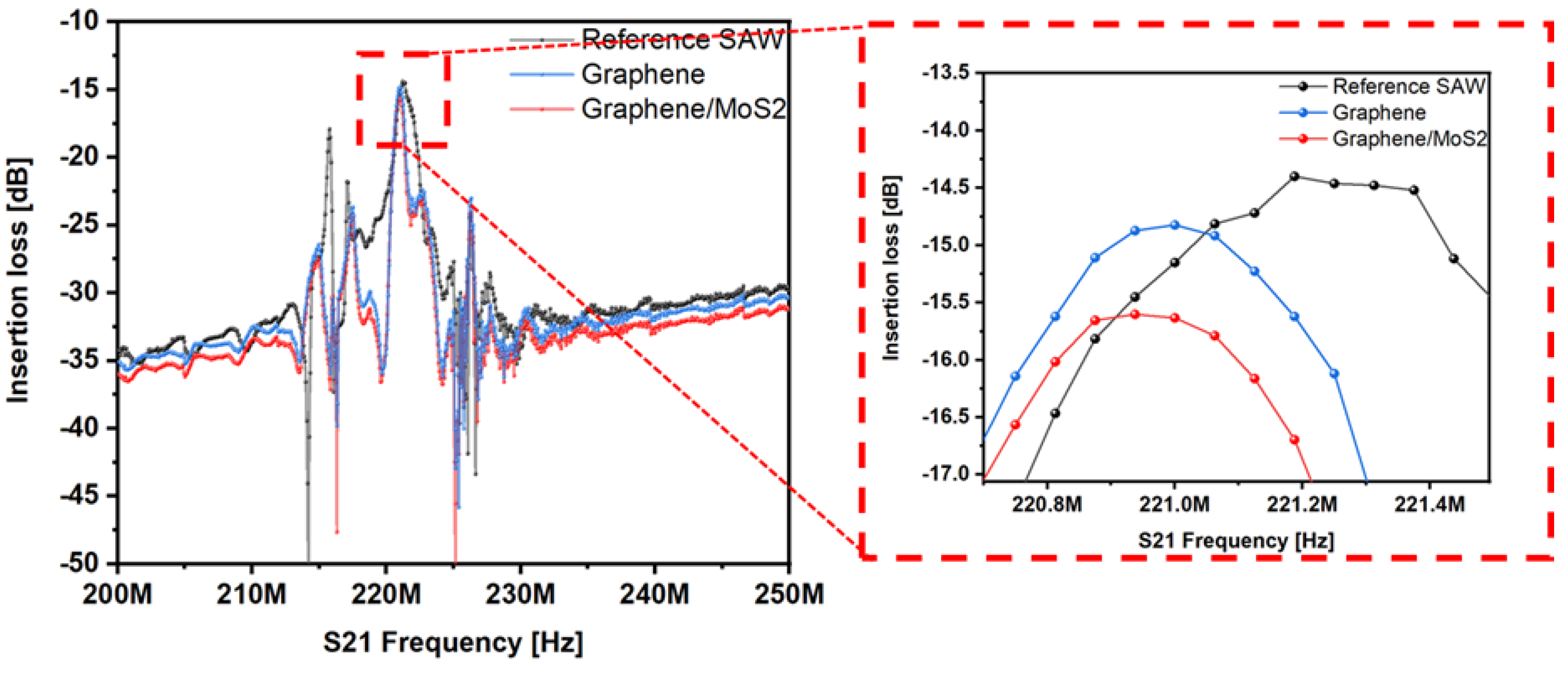
4.1. Fabricated SAW Sensor

Figure 6 shows the fabricated SAW-based NO2 sensor. A two-port SAW delay line was formed on a 128° YX LiNbO3 substrate, and the 2D monolayer graphene/MoS2 were transferred to the cavity region between the two IDTs. The Pt-based microheater and temperature sensor are located near the cavity of the two-port SAW delay line. Figure 6 presents the scanning electron microscopy (SEM) image and energy-dispersive X-ray spectroscopy (EDX) analysis of the MoS2 flake transferred onto the cavity region of the SAW device, along with the MoS2 film deposited by RF sputtering. Stable film formation was confirmed, and the Mo:S composition ratio in the film was estimated to be 56:43.

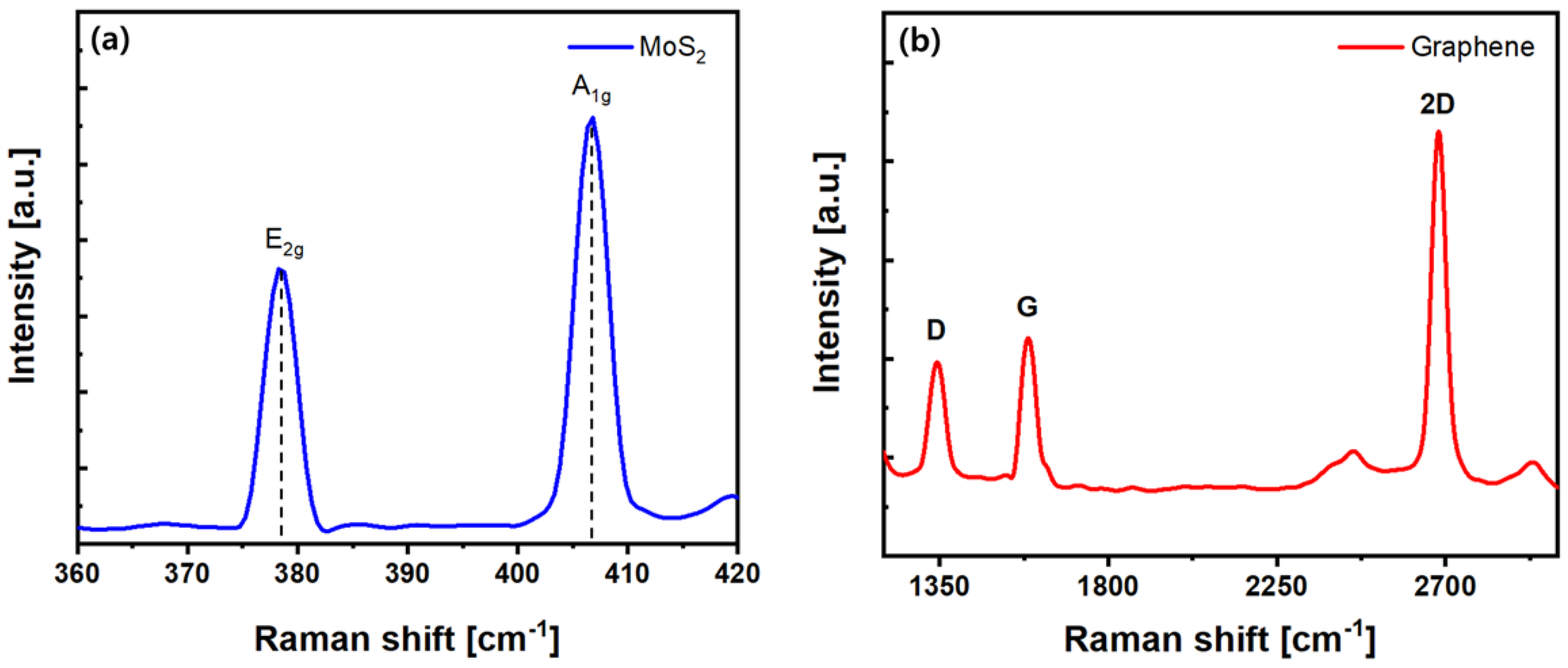
4.2. Analysis of the NO2 Sensing Material

To determine the structural characteristics of the deposited MoS2, including its layer number, phase, and defect density, Raman spectroscopy analysis was conducted. Figure 7 shows the Raman peaks of the deposited MoS2, with two prominent peaks observed at approximately 378 cm−1 (E2g) and 406 cm−1 (A1g), resulting in a separation of ~28 cm−1. Based on these, the deposited MoS2 was identified as the hexagonal phase and confirmed to be multilayer. The extent of defects in the MoS2 film can also be inferred from the positions and intensities of the D-band and D2-band. However, the intensities of these peaks in the deposited MoS2 film are minimal, indicating a low defect density in the material. Next, the Raman spectrum of graphene was analyzed, revealing the D, G, and 2D peaks at approximately 1350, 1580, and 2700 cm−1, respectively. The D band (around 1350 cm−1) is a disorder-related peak that is activated by defects or edges in the graphene lattice. A weak intensity in the D band was observed, indicating the presence of some defects, though it is minimal. The intensity ratio of the G band to the 2D band can be used to determine the number of graphene layers. The I2D/IG ratio was greater than 2, confirming that the deposited graphene is monolayer.

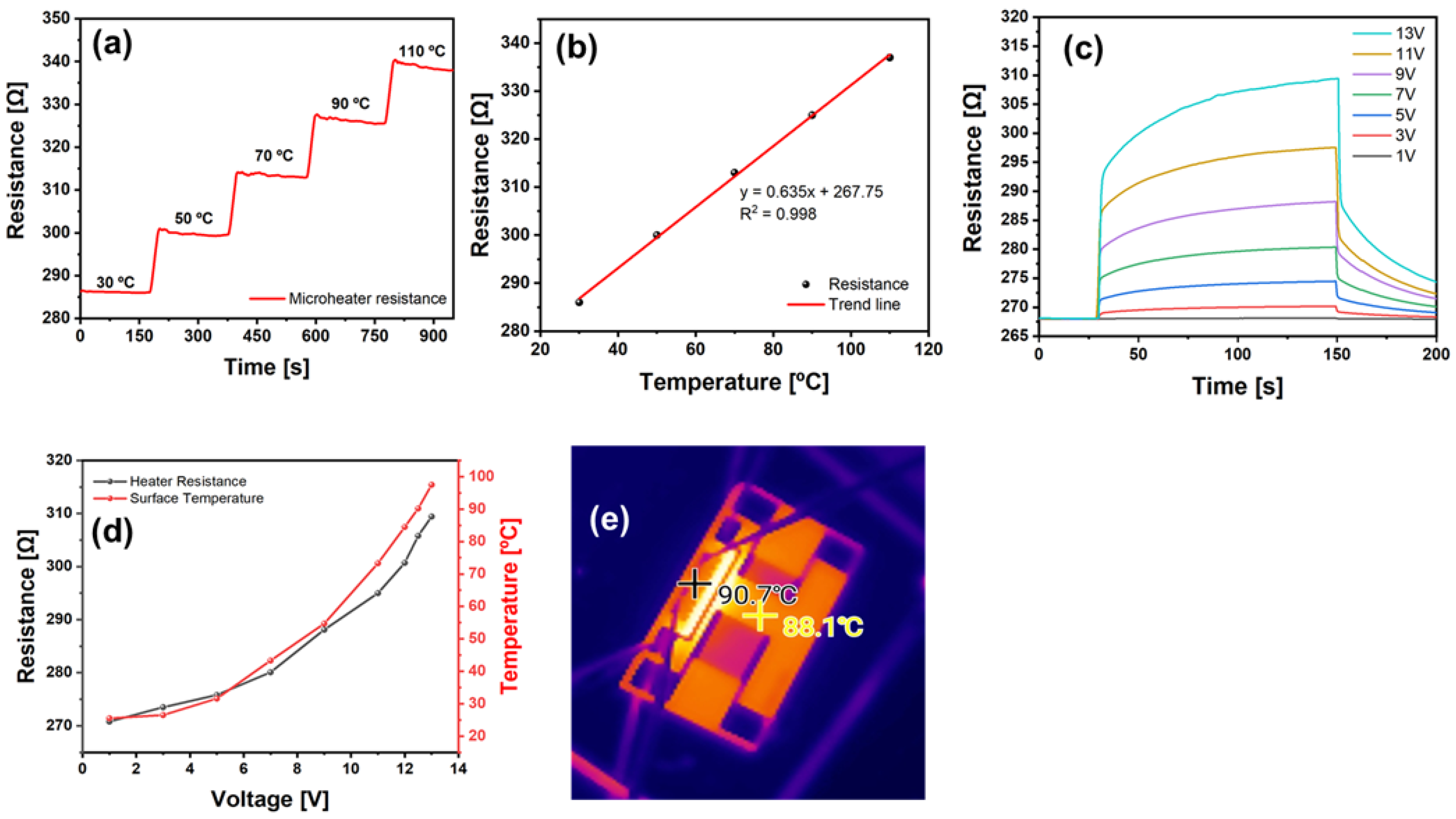
4.3. Microheater Characterization

To enhance the sensor’s sensitivity and selectivity and to achieve ultra-fast response and recovery times, a microheater and a temperature sensor were integrated into the SAW sensor. The temperature sensor is specifically used to monitor the performance of the microheater. For calibration, a known external temperature is applied, and the resistance of the temperature sensor is measured. Then, voltage is applied to the microheater, and the corresponding resistance change in the temperature sensor is monitored to assess the temperature variation induced by the microheater. During testing, the sensor was integrated into the microprobe system (NEXTRON Co., Busan, Republic of Korea), and external temperatures were applied using the MPS temperature controller (NEXTRON Co.). Resistance changes were measured with respect to the externally applied temperature to establish a calibration dataset for future experiments involving voltage application. The measurement system consisted of a chamber equipped with a microprobe system (NEXTRON Co.), a controller (NEXTRON Co.), and a power supply to regulate the sensor surface temperature by applying voltage to the microheater. A source meter (Keithley-2400, Seoul, Republic of Korea) was used to precisely measure the resistance of the sensor. The voltage was supplied through a 4-probe connection, and the change in resistance was monitored using the source meter. Temperature control was managed via the NEXTRON automated program. Data from the temperature sensor were analyzed in real time and saved for calibration purposes. The resistance–temperature correlation data, which are critical for calibrating voltage-driven thermal responses, are presented already in detail in the manuscript. Figure 8 illustrates the temperature change on the SAW sensor surface when voltage is applied to the integrated microheater. As shown in Figure 8a, the resistance of the temperature sensor increases with externally applied temperature, confirming its sensitivity to temperature variations. Figure 8b presents the calibrated temperature sensor response, demonstrating a linear trend with a high coefficient of determination (R2 = 0.998), ensuring accurate temperature measurement. Figure 8c depicts the temperature variation of the microheater at different applied voltages, confirming that the temperature reaches 90 °C with a 12.5 V input to the microheater (calibrated through the resistance change in the temperature sensor), which is slightly different than the simulation result because of differences between the simulated and real-world conditions, such as heat loss, material properties, and experimental setup variations. This figure further confirms the microheater’s response time and long-term stability as a function of applied voltage, showing that the temperature remains steady and approaches a stable condition (rather than saturation). Figure 8d presents the temperature measurements on the sensor surface and calibrated resistance change measurements of the temperature sensor. The power consumed by the microheater at 12.5 V is 2.5 W. Additionally, the temperature change detected by the temperature sensor quickly reaches stability. Once this is achieved, the temperature remains stable for an extended period, demonstrating rapid recovery time and excellent repeatability, as confirmed by the integrated temperature sensor. Figure 8e shows the temperature distribution across the entire SAW sensor surface, captured by an infrared camera (FLIR C5, Seoul, Republic of Korea), in response to the applied voltage to the microheater. The emissivity value used to measure the temperature was set to 0.8, as MoS2/graphene composites typically have emissivity values around 0.8 [30,31,32,33]. A theoretical model explaining the thermodynamics of multi-material properties is discussed in other studies [30,31,32,33]. With a 12.5 V input to the microheater, the temperature at the center of the cavity reaches 90 °C and remains stable under steady-state conditions.

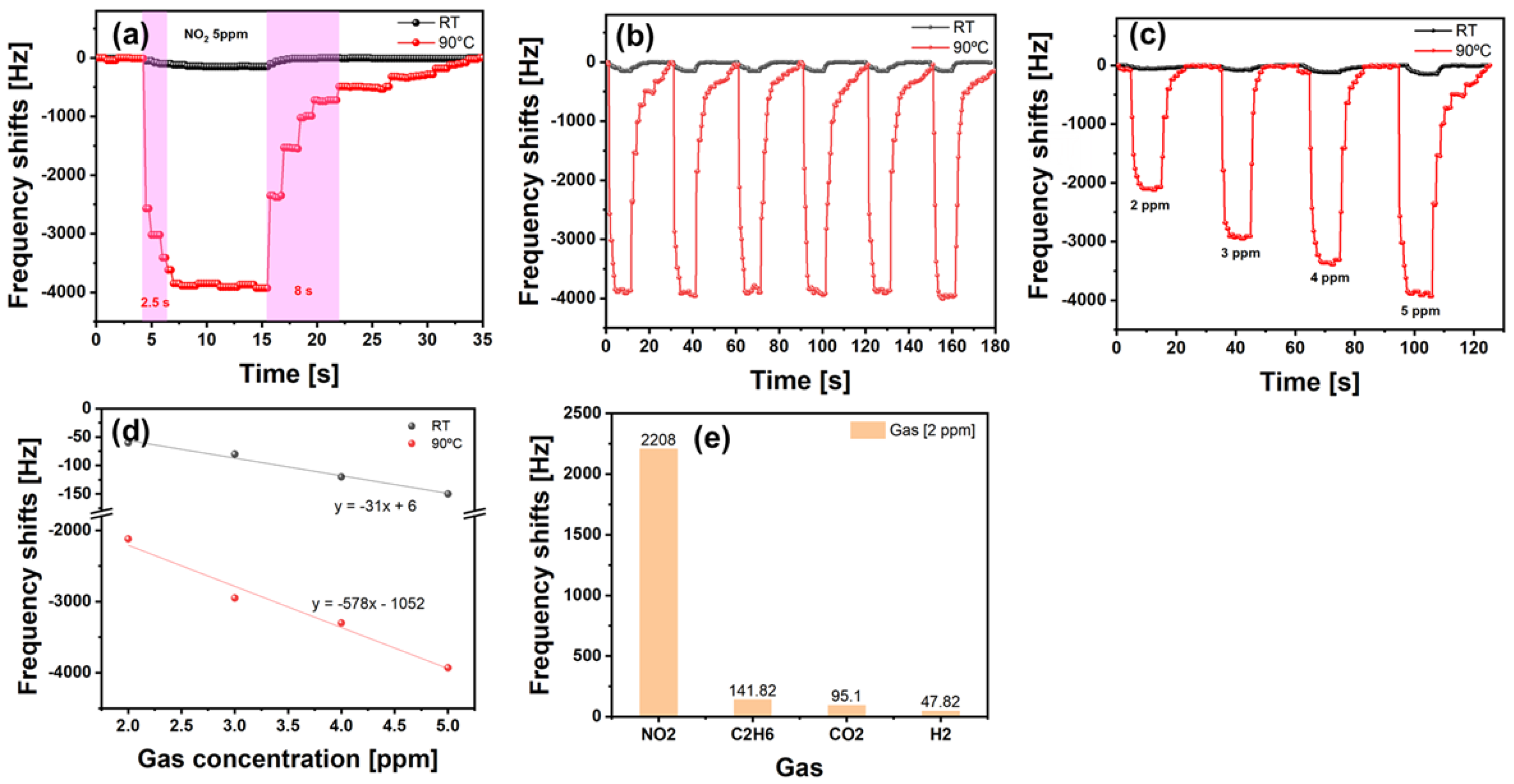
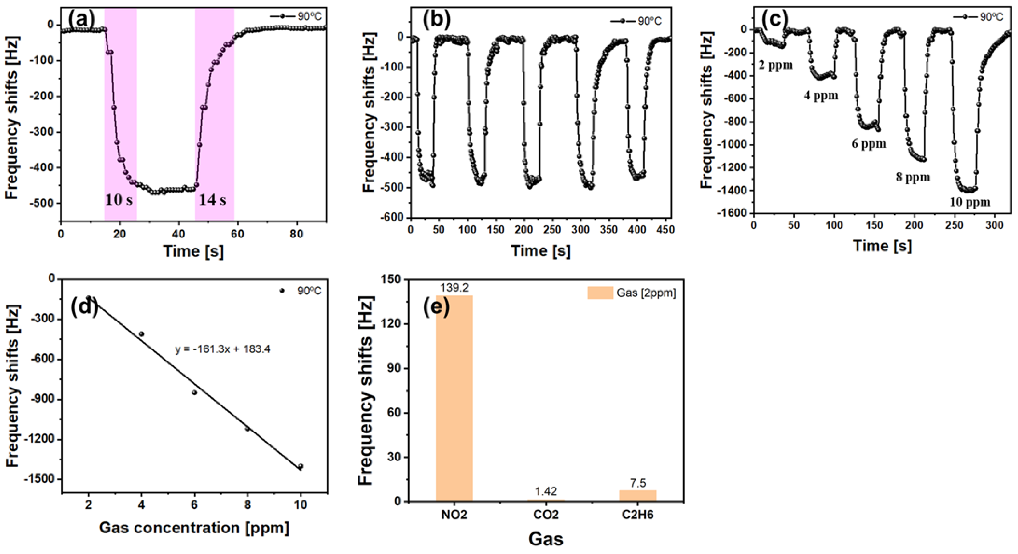
4.4. Sensor Characterizations with Interface Electronics

The fabricated sensor was first measured using a network analyzer. As predicted by COM modeling, it exhibited a center frequency of 222 MHz, low insertion loss (14 dB), and minimal parasitic conductance in the high-frequency range (Figure 9). Owing to the transferred sensing material, a slight downshift in the center frequency and an increase in insertion loss were observed. To preserve the accurate characteristics of our developed interface electronics, the insertion loss must remain below 18 dB.
Two sensors with different sensing materials are fabricated and characterized to compare their properties as a function of the sensing material’s volume (thickness). The first sensor is a heterostructure combining graphene and MoS2 flakes grown by CVD, while the second sensor is a heterostructure combining graphene and MoS2 film grown by RF magnetron sputtering. The sensors are placed in a chamber, where a 5 V DC voltage is applied to the oscillator, and the output frequency is stabilized for an extended period in an N2 environment. Two operating temperatures are tested, room temperature (RT) and 90 °C. The maximum temperature is set to 90 °C to minimize changes in the piezoelectric properties of LiNbO3 and to prevent degassing from the sensor. NO2 gas is injected into the chamber through an MFC, while N2 gas is used as the control (blank) gas. Figure 10 shows the sensor characteristics, including the graphene/MoS2 flake sensing material, in response to varying NO2 concentrations (2–5 ppm) at both RT and 90 °C. Despite the low NO2 concentration (2 to 5 ppm), a substantial frequency change and fast response time are observed at 90 °C, owing to the combined effects of significant changes in the conductivity of the monolayered 2D material and the mass loading effect. As the temperature rises to 90 °C, both the frequency change and response time improve markedly. At RT, the frequency change for 1 ppm (sensitivity) was 31 Hz/ppm, while at 90 °C, the frequency change significantly increased to 578 Hz/ppm.
The evaluated sensor’s response time to reach 90% of the saturation value at 90 °C for 5 ppm was 2.5 s. These characteristics represent the highest performance reported to date among SAW-based sensors (see Table 3), to the best of my knowledge. While NO2 sensors typically exhibit long recovery times, the recovery time in this study to reach 10% of the saturation value at 90 °C for 5 ppm was measured at 8 s. This rapid recovery is attributed to the minimized defects in the NO2 sensing material, the weak interaction between the sensing material and the NO2 gas, and the increased desorption energy provided by the microheater. The repeatability of the sensor’s characteristics was assessed at 90 °C for 5 ppm over five cycles, with nearly identical frequency changes, response times, and consistency observed across all cycles. The sensor’s selectivity to gases similar to those found in spacecraft was evaluated, with the concentrations of the tested gases remaining within the spacecraft’s allowable range. As shown in Figure 10, at 90 °C and a 2 ppm NO2 concentration, the sensor exhibited a significant frequency shift of approximately 2208 Hz, while only minimal changes were observed for C2H6, CO2, and H2 gases. This suggests that the developed sensor exhibits high selectivity for NO2, which can be attributed to the highly reactive sensing material and its optimized operating temperature.
For comparison of the sensor properties in terms of the internal volume of the sensing material, the sensor with a graphene/MoS2 film as the sensing material was also characterized (Figure 11). The entire measurement process was carried out in the same manner as for the previously mentioned sensor. At room temperature, the sensor’s signal-to-noise ratio (SNR) is too low to enable measurements. Using a microheater, the temperature was set to 90 °C, and a 5 ppm NO2 concentration was applied. A significant frequency shift of 500 Hz was observed, along with a fast response time of 10 s and a recovery time of 14 s. The sensitivity, evaluated from the calibration plot for NO2 concentrations in the range of 2–10 ppm, was −161.3 Hz/ppm (Figure 11a). Compared to the initially measured sensor with graphene/MoS2 flakes, the frequency shift and response time of the graphene/MoS2 film sensor were slightly worse. This degradation can be attributed to several factors, including the MoS2 film, which covers the entire sensing surface and limits the carrier changes in the graphene beneath it. Additionally, the increased total mass of the sensing material results in smaller percentage changes in mass due to NO2 gas adsorption. The minimum detection limit (MDL) was approximately 300 ppb, based on the concentration of NO2 that produced a signal three times the standard deviation of the blank (without NO2). The repeatability characteristics were measured over five cycles at a concentration of 5 ppm. Almost identical responsiveness was observed in all cycles, confirming stable repeatability. The evaluated sensitivity was 161 Hz/ppm at 90 °C, which is lower than that of the sensor with graphene/MoS2 flakes as the sensing material (Figure 11d). A selectivity test was conducted using gases that coexist inside spacecraft. The developed sensor exhibited a significant frequency change of 139 Hz for 2 ppm NO2, while CO2 and C2H6 caused only minimal frequency shifts of 1.42 Hz and 7.5 Hz, respectively, at the same 2 ppm concentration (Figure 11e).
Table 3 presents a comparison of the characteristics between the two types of sensors we developed and the existing SAW sensors reported in the literature. The reported SAW gas sensors suffer from long response and recovery times, ranging from tens to hundreds of seconds. In contrast, our SAW sensors with temperature control demonstrate superior performance, particularly in terms of response and recovery times at 90 °C. Additionally, the sensor utilizing graphene/MoS2 flakes as the sensing material outperforms the sensor with a graphene/MoS2 film in terms of sensitivity and response/recovery time. This improvement is attributed to the rapid saturation of NO2 gas on the monolayers, high mobility, and the enhanced combined hybrid effects of conductivity and mass loading.

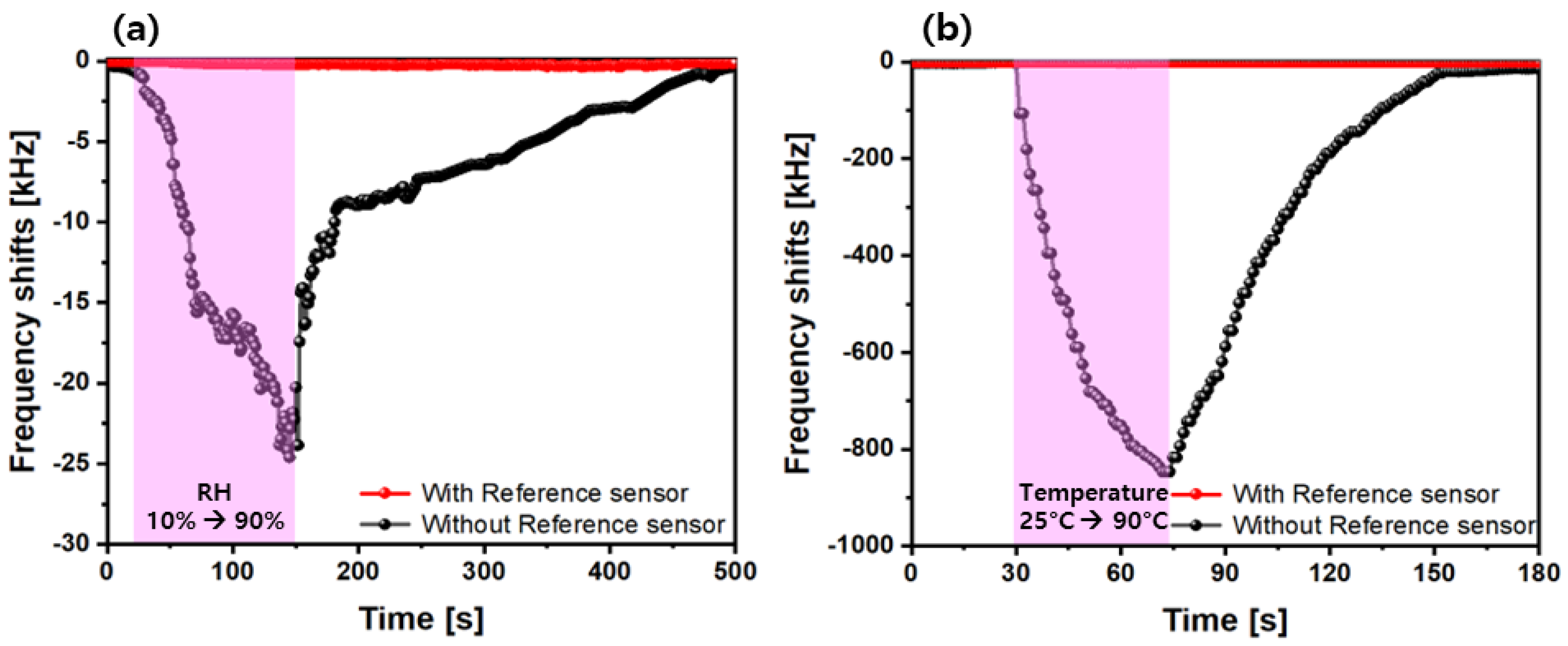
4.5. Humidity/Temperature Compensations via Interface Electronics

The changes in ambient humidity and temperature affect the center frequencies of both the SAW sensor and the reference SAW device equally. By subtracting the frequency shifts from both devices at the mixer, the system can provide built-in compensation that eliminates output frequency shifts caused by variations in ambient temperature and humidity. Two separate experimental tests were conducted to confirm the effectiveness of this built-in compensation. First, the signal generator is connected to the port of the reference SAW device at the mixer. A change in relative humidity (RH) from 10% to 90% causes a significant frequency shift of up to 25 kHz when a constant signal from the signal generator is used as the reference (Figure 12a). This large shift makes it difficult to accurately observe NO2 gas responses due to the influence of humidity. In contrast, when the reference SAW device, with performance identical to the SAW sensor, is used, no noticeable frequency change is observed due to humidity variations, and no frequency shifts are detected at the output. A similar trend was observed for temperature changes. Although the LiNbO3 substrate is sensitive to temperature, the temperature variations are identical in both SAW devices. By subtracting these variations in the mixer, it was confirmed that no change occurs in the output due to ambient temperature fluctuations. Additionally, when the surface temperature of the two SAW devices was raised to 90 °C, and the ambient temperature was lower than the surface temperature of the devices, the output signals from both devices showed no change, owing to the built-in compensation (Figure 12b).

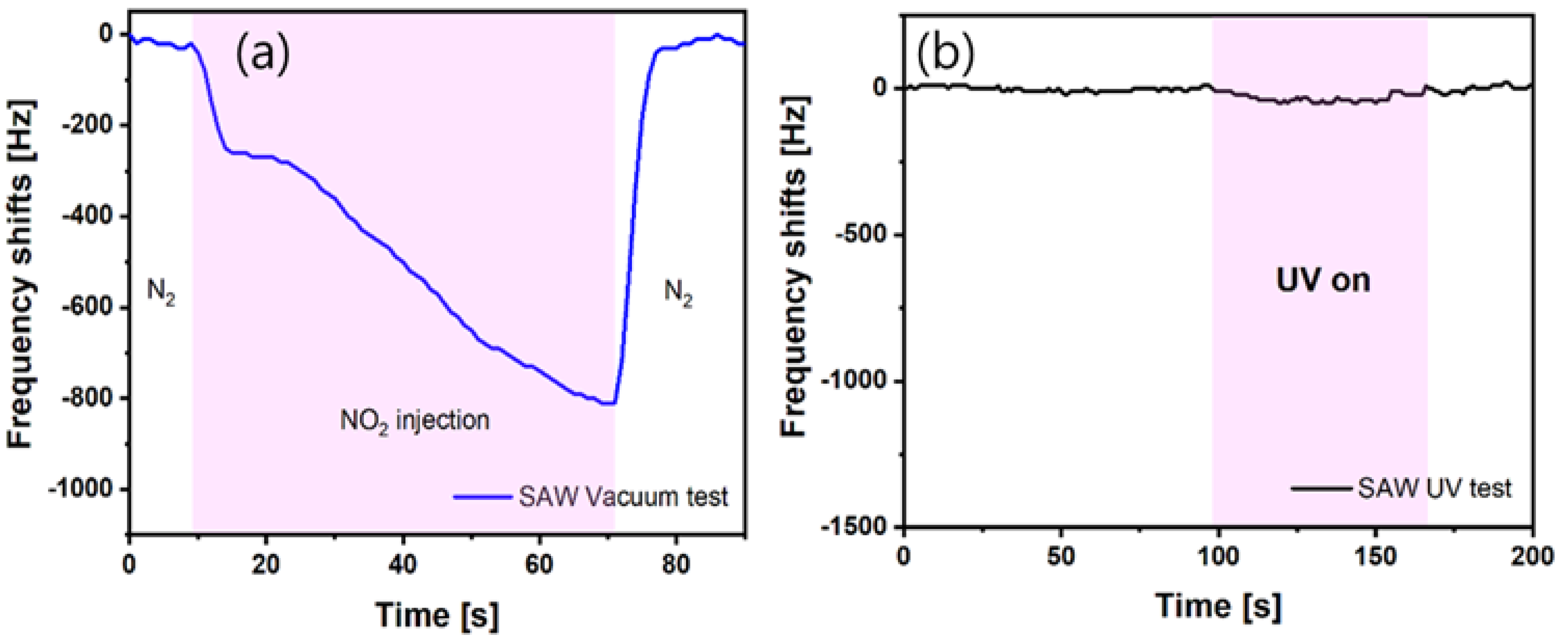
4.6. Field Test Simulating Space Environment

The sensor’s operation must be verified under oxygen-free conditions on the sensor’s surface and exposure to UV-C radiation for use in spacecraft. To test its usability in an oxygen-free environment, the measurement chamber was kept in a vacuum for an extended period. Then, nitrogen (N2) was introduced to remove any oxygen adsorbed on the surface of the sensing material. Following this, NO2 gas was introduced to the sensor surface with increasing concentration over 60 s, and a significant frequency change, consistent with the calibration tests, was observed (Figure 13a). This confirmed that the sensor operates effectively, even in the absence of oxygen. Afterward, when nitrogen (N2) was injected as the control gas, the sensor’s output frequency returned to its original state. The same frequency change was observed across multiple cycles, further confirming the sensor’s reliability in an oxygen-free environment.
Additionally, the sensor was tested under UV-C illumination, and no frequency change was observed, thanks to the built-in compensation system of the two sensors (Figure 13b). Future studies will focus on examining the sensor’s characteristics under gravity-free conditions.

5. Conclusions

We have presented the development of a SAW-based NO2 sensor and its interface electronics for monitoring NO2 gas within spacecraft. The sensor consists of a two-port SAW delay line with 2D sensing materials positioned between two IDTs. Single-layer graphene and MoS2 are used as sensing materials for NO2 detection due to their high surface-to-volume ratio, high mobility, and moderate bonding with target molecules. The interface electronics, which include two oscillators, a mixer, an LPF, a comparator, an FPGA, and a PC, feature a built-in compensation circuit to mitigate output frequency shifts caused by variations in ambient temperature and humidity. The sensor was successfully verified to operate effectively under oxygen-free conditions and UV-C radiation, making it highly suitable for NO2 measurement in spacecraft.

Author Contributions

F.N.: conceptualization, methodology, data curation, formal analysis, writing—original draft. H.L.: conceptualization, methodology, data curation, formal analysis, writing—original draft. F.N. and H.L. contributed equally to this work as first co-authors. W.W.: data curation, funding acquisition. K.L.: conceptualization, methodology, writing—original draft, project administration, funding acquisition. All authors have read and agreed to the published version of the manuscript.

Funding

This research was funded by the Ministry of Science and ICT (RS-2023-00278288 and RS-2024-00457846).

Institutional Review Board Statement

Not applicable.

Informed Consent Statement

Not applicable.

Data Availability Statement

The raw data supporting the conclusions of this article will be made available by the authors on request.

Conflicts of Interest

The authors declare no conflicts of interest.

References

  1. Perry, J.L.; George, J.L. Spacecraft Cabin Air Quality Control and Its Application to Tight Buildings. AIAA J. 1995, 95, 1050. [Google Scholar]
  2. James, J.T.; Limero, T.F. Air Quality in NASA’s Manned Spacecraft: The Artemis Challenge. Aerosp. Med. Hum. Perform. 2021, 92, 537–550. [Google Scholar]
  3. Jones, B.W.; Mason, E.A. Spacecraft Cabin Air Contaminants and Their Control. J. Spacecr. Rocket. 1985, 22, 25–33. [Google Scholar]
  4. Limero, T.F.; Wilson, T. Off-Gassing and Trace Contaminants in Manned Spacecraft Environments. Aerospace Med. Hum. Perform. 2018, 89, 567–575. [Google Scholar]
  5. James, J.T.; Gardner, D.P. Spacecraft Maximum Allowable Concentrations for Airborne Contaminants: 2020 Update; NASA Technical Reports; NASA/TP-2020-50001913; National Aeronautics and Space Administration: Washington, DC, USA, 2020.
  6. Frampton, M.W.; Boscia, J.; Roberts, N.J. Nitrogen Dioxide Exposure: Effects on Airway and Immune Cells. Am. J. Respir. Crit. Care Med. 2002, 166, 1298–1305. [Google Scholar]
  7. Seinfeld, J.H.; Pandis, S.N. Atmospheric Chemistry and Physics: From Air Pollution to Climate Change, 3rd ed.; Wiley-Interscience: Hoboken, NJ, USA, 2016; pp. 872–880. [Google Scholar]
  8. Devlin, R.B.; Horstman, D.P.; Gerrity, T.R. NO2 Effects on Lung Function and Airway Inflammation. Am. J. Respir. Crit. Care Med. 1999, 159, 315–325. [Google Scholar]
  9. Tunnicliffe, W.S.; Harrison, R.M.; Kelly, F.J. NO2 Exposure and Effects on Lung Inflammation and Cardiovascular Function. Thorax 2001, 56, 567–574. [Google Scholar]
  10. Yang, S.; Li, Y.; Wang, C.; Xie, G. Recent Advances in NO2 Gas Sensors: Challenges and Future Directions. Sensors 2020, 20, 3147. [Google Scholar]
  11. Verma, A.; Prasad, M. 2D Materials for Gas Sensing Applications: A Review on Graphene Oxide, MoS2, WS2 and Phosphorene. Nanomaterials 2018, 8, 736. [Google Scholar]
  12. Liu, C.; Zhou, Y. Highly Sensitive NO2 Gas Sensors Based on MoS2@MoO3 Ferromagnetic Heterostructures. Nanomaterials 2022, 12, 1441. [Google Scholar]
  13. Zhang, H.; Wang, J. Robust Room-Temperature NO2 Sensors from Exfoliated 2D Few-Layered WSe2 Field-Effect Transistors. ACS Appl. Mater. Interfaces 2021, 13, 12334–12344. [Google Scholar]
  14. Sharma, S.; Kumar, N. A Systematic Review on 2D MoS2 for Nitrogen Dioxide (NO2) Sensing at Room Temperature. Mater. Today Commun. 2020, 25, 101586. [Google Scholar]
  15. Lee, H.; Park, Y. Strategies and Challenges for Improving the Performance of Two-Dimensional Material-Based Gas Sensors. Emerg. Mater. Res. 2023, 12, 2288353. [Google Scholar]
  16. Smith, A.; Brown, K. Unencapsulated and Washable Two-Dimensional Material Electronic Textiles for Health and Environmental Monitoring. Sci. Rep. 2022, 12, 13002. [Google Scholar]
  17. Kim, D.; Lee, J. Mechanisms of NO2 Detection in Hybrid Structures Containing Reduced Graphene Oxide. Sensors 2022, 22, 5316. [Google Scholar] [CrossRef]
  18. Park, T.; Choi, H. Chemical Sensing of 2D Graphene/MoS2 Heterostructure Device. ACS Appl. Mater. Interfaces 2015, 7, 19295–19304. [Google Scholar]
  19. Zhao, Y.; Wang, S. Graphene-Based Sensors for Detecting NO2 at Room Temperature. Sensors 2020, 20, 3175. [Google Scholar]
  20. Lin, J.; Zhu, L. Enhanced NO2 Gas Sensing Performance of MoS2 Nanosheets by Surface Decoration with Au Nanoparticles. Sensors 2019, 19, 1296. [Google Scholar]
  21. Zhang, R.; Zhou, Z.; Shi, L. NO2 Sensing Mechanisms of 2D Transition Metal Dichalcogenide Materials: A First-Principles Study. J. Phys. Chem. C 2022, 126, 5460–5471. [Google Scholar]
  22. Zhang, C.; Wang, Y.; Li, H. High-Performance MoS2-Based Gas Sensors for NO2 Detection at Room Temperature. ACS Sens. 2019, 4, 2171–2180. [Google Scholar]
  23. Castro Neto, A.H.; Guinea, F.; Peres, N.M.R. The Electronic Properties of Graphene. Rev. Mod. Phys. 2009, 81, 109–162. [Google Scholar]
  24. Liu, B.; Wang, X.; Sun, H. Two-Dimensional MoS2-Based Composite Materials for High-Performance Gas Sensors. J. Mater. Chem. C 2021, 9, 5475–5487. [Google Scholar]
  25. Cheng, X.; Tang, W.; Ma, X. The Influence of Defects on NO2 Sensing Performance of 2D Materials: A Density Functional Theory Study. J. Phys. Chem. C 2023, 127, 2340–2350. [Google Scholar]
  26. Ma, X.; Tang, W.; Cheng, X. Recent Advances in 2D NO2 Sensing Materials: Performance, Mechanisms, and Challenges. ACS Appl. Mater. Interfaces 2023, 15, 20345–20360. [Google Scholar]
  27. Nawaz, F.; Kim, S.; Lee, H.; Park, J.; Song, J.; Choi, C.; Lee, K. Toward Ultra-Fast Response and Recovery Characteristics through ZnO Multilayer Thin Films in Surface Acoustic Wave UV Sensor. IEEE Sens. J. 2025, 25, 343–353. [Google Scholar]
  28. Kim, S.; Nawaz, F.; Choi, C.; Jeon, I.; Lee, K. Synthesis and Characterization of High-Quality Ta2O5 Nanoparticles for Highly Selective SAW-Based DUV Sensor and Corona Detection Application. Adv. Mater. Technol. 2024, 9, 2301486. [Google Scholar]
  29. Kondalkar, V.; Li, X.; Park, I.; Yang, S.; Lee, K. Development of Chipless Wireless Current Sensor System based on Giant Magnetoimpedance Magnetic Sensor and Surface Acoustic Wave Transponder. Sci. Rep. 2018, 8, 2401. [Google Scholar]
  30. Yalon, E.; McClellan, C.J.; Smithe, K.K.H.; Muñoz Rojo, M.; Xu, R.L.; Suryavanshi, S.V.; Gabourie, A.J.; Neumann, C.M.; Xiong, F.; Farimani, A.B.; et al. Energy Dissipation in Monolayer MoS2 Electronics. Nano Lett. 2017, 17, 3429–3433. [Google Scholar] [CrossRef]
  31. Balandin, A.A. Thermal Properties of Graphene and Nanostructured Carbon Materials. Nat. Mater. 2011, 10, 569–581. [Google Scholar] [CrossRef]
  32. Shiue, R.-J.; Gao, Y.; Tan, C.; Peng, C.; Zheng, J.; Efetov, D.K.; Kim, Y.D.; Hone, J.; Englund, D. Thermal Radiation Control from Hot Graphene Electrons Coupled to a Photonic Crystal Nanocavity. Nat. Commun. 2019, 10, 109. [Google Scholar] [CrossRef]
  33. Chen, X.-K.; Zeng, Y.-J.; Chen, K.-Q. Thermal Transport in Two-Dimensional Heterostructures. Front. Mater. 2020, 7, 578791. [Google Scholar] [CrossRef]
  34. Pasupuleti, K.S.; Reddeppa, M.; Chougule, S.S.; Bak, N.; Nam, D.-J.; Jung, N.; Cho, H.D.; Kim, S.-G.; Kim, M.-D. High Performance Langasite Based SAW NO2 Gas Sensor Using 2D G-C3N4@TiO2 Hybrid Nanocomposite. J. Hazard. Mater. 2022, 427, 128174. [Google Scholar] [PubMed]
  35. Xiong, S.; Zhou, J.; Wu, J.; Li, H.; Zhao, W.; He, C.; Liu, Y.; Chen, Y.; Fu, Y.; Duan, H. High Performance Acoustic Wave Nitrogen Dioxide Sensor with Ultraviolet Activated 3D Porous Architecture of Ag-Decorated Reduced Graphene Oxide and Polypyrrole Aerogel. ACS Appl. Mater. Interfaces 2021, 13, 42094–42103. [Google Scholar] [PubMed]
  36. Pasupuleti, K.S.; Reddeppa, M.; Nam, D.-J.; Bak, N.-H.; Peta, K.R.; Cho, H.D.; Kim, S.-G.; Kim, M.-D. Boosting of NO2 Gas Sensing Performances Using GO-PEDOT:PSS Nanocomposite Chemical Interface Coated on Langasite-Based Surface Acoustic Wave Sensor. Sens. Actuators B Chem. 2021, 344, 130267. [Google Scholar]
  37. Sadek, A.Z.; Wlodarski, W.; Kalantar-zadeh, K.; Powell, D.A.; Hughes, W.L.; Buchine, B.A.; Wang, Z.L. H2 and NO2 Gas Sensors with ZnO Nanobelt Layer on 36° LiTaO3 and 64° LiNbO3 SAW Transducers. IEEE Sens. J. 2005, 5, 1343–1346. [Google Scholar]
Figure 1. Overall schematic of the microheater-integrated SAW sensor and interface electronics.
Applsci 15 04050 g001
Figure 2. (a) The detailed schematic of the developed SAW sensor and (b) its COM modeling results for S21 vs. frequency, with and without the sensing materials.
Applsci 15 04050 g002
Figure 3. Heat conduction through the medium from the microheater and the evaluation of the temperature at the center of the cavity as a function of the applied voltage to the microheater.
Applsci 15 04050 g003
Figure 4. The fabrication procedure of the two-port SAW delay line, graphene/MoS2 flake transfer, and microheater.
Applsci 15 04050 g004
Figure 5. (a) Schematic and (b) optical images of the testing setup.
Applsci 15 04050 g005
Figure 6. (a) Optical image of the fabricated NO2 sensor, SEM images of (b) graphene, (c) MoS2 flake, (d) MoS2 film, and (e) EDX analysis of the MoS2 film deposited by RF sputtering.
Applsci 15 04050 g006
Figure 7. Raman peaks of (a) the deposited MoS2 film and (b) the transferred graphene.
Applsci 15 04050 g007
Figure 8. (a) Resistance variation of the temperature sensor as a function of externally applied temperature, (b) calibrated output of the temperature sensor, (c) response and recovery times of the temperature sensor resistance as a function of applied voltage to the microheater, (d) temperature of the microheater as a function of applied voltage, measured at the temperature sensor location and surface, and (e) heat distribution on the sensor surface induced by a 12.5 V DC voltage applied to the microheater, captured using an infrared camera.
Applsci 15 04050 g008
Figure 9. The S21 scattering parameter as a function of frequency, measured using a network analyzer.
Applsci 15 04050 g009
Figure 10. (a) Response and recovery of 5 ppm NO2 on graphene/MoS2 flakes SAW sensor, (b) repeatability of 5 ppm NO2 on SAW sensor, (c) response to 2–5 ppm NO2 on SAW sensor, (d) calibration plot for different NO2 concentrations on SAW sensor, and (e) selectivity of SAW sensor.
Applsci 15 04050 g010
Figure 11. (a) Response and recovery of 5 ppm NO2 on graphene/MoS2 flakes SAW sensor at 90 °C, (b) repeatability of 5 ppm NO2 on SAW sensor, (c) response to 2–10 ppm NO2 on SAW sensor, (d) calibration plot for different NO2 concentrations on SAW sensor, and (e) selectivity of SAW sensor.
Applsci 15 04050 g011
Figure 12. Frequency variations in the sensor system, with and without reference SAW devices. (a) Frequency variations in relative humidity (RH) from 10% to 90% RH and (b) frequency changes in temperature from 25 °C to 90 °C.
Applsci 15 04050 g012
Figure 13. Frequency variation of the sensor due to (a) NO2 infusion in an oxygen-free environment and (b) exposure to UV-C radiation.
Applsci 15 04050 g013
Table 1. Main hazardous gases and their respective allowable concentration limits within the spacecraft.
GasFormula10-Day SMAC ppm6-h SMAC ppm
HydrogenH2300012,000
Carbon dioxideCO2700013,000
EthanolCH3CH2OH2401000
MethaneCH450005000
2-propanolCH3CH[OH]CH350500
DichloromethaneCH2Cl25100
TolueneC6H5CH320100
Carbon monoxideCO2050
TrichloroethyleneCHCl CCl21250
AmmoniaNH32525
BenzeneC6H6210
Nitric dioxideNO20.5-
Table 2. The parameters of the two-port SAW delay line determined through COM modeling.
ParameterValue
Number of input and output IDT pairs60
Number of reflector pairs80
Aperture length (λ)120
Cavity length (μm)2000
Wavelength λ (μm)17.6
IDT Ti/Pt thickness (nm)10/100
Acoustic velocity (m/s) of 128° YX LiNbO33890
Electromechanical coupling factor, K2 (%)5.5
Effective dielectric coefficient εp055
Sheet resistance (Ω-m)0.939 × 10⁸
Table 3. Comparison of response/recovery time and sensitivity in SAW-based NO2 sensors from previous studies.
Sensing MaterialCenter Freq.
(MHz)
Res.
(kHz/ppm)
Res./Rec.
Time (s)
Temp.Ref.
TiO2 NP135.88.5/100310/182RT[34]
g-C3N4@TiO2 NP135.719.7/100143/114RT[34]
Ag/rGO-ppy246.9913.2/10068/190RT[35]
GO-PEDOT:PSS135.785.7/10035/10RT[36]
ZnO nano belt1113.5/1090/140160 °C[37]
Graphene/MoS2 film2220.14/210/1490 °CThis work
Graphene/MoS2 flakes2222.1/22.5/890 °CThis work
Disclaimer/Publisher’s Note: The statements, opinions and data contained in all publications are solely those of the individual author(s) and contributor(s) and not of MDPI and/or the editor(s). MDPI and/or the editor(s) disclaim responsibility for any injury to people or property resulting from any ideas, methods, instructions or products referred to in the content.

