Article

Research on Lifespan Prediction Methods Using Ultrasonic Microimaging for Electronic Packaging

1
School of Mechanical Engineering, Xi’an University of Science and Technology, Xi’an 710054, China
2
School of Mechanical Engineering, Liverpool John Moores University, Liverpool L3 3AF, UK
*
Author to whom correspondence should be addressed.
Appl. Sci. 2025, 15(6), 3246; https://doi.org/10.3390/app15063246
Submission received: 8 February 2025 / Revised: 3 March 2025 / Accepted: 13 March 2025 / Published: 17 March 2025

Abstract

:
Addressing the issue of lifespan prediction for electronic packages under thermal loading, this paper proposes a method for predicting the lifespan of electronic packages based on ultrasonic microimaging. Firstly, experimental samples equipped with flip-chip packages were designed and fabricated and subjected to aging through thermal cycle acceleration tests. Ultrasonic microscopy was utilized to periodically acquire ultrasonic image data for monitoring solder joint degradation. Secondly, the internal ultrasonic wave propagation mechanism within electronic packages was investigated, establishing a qualitative relationship between the intensity in the central region of the solder joint’s ultrasonic image and internal defects within the joint. Image processing techniques were applied to enhance the quality of the solder joint images, and the mean intensity in the central region of the solder joint image was extracted as a failure feature. Finally, based on the extracted failure feature, a data-driven failure model for solder joints was developed, which predicts the lifespan of the solder joints based on cumulative failure probability. The research results indicate that the proposed model accurately describes the failure process of solder joints and effectively differentiates the lifespan variations among solder joints at different locations on the chip. This provides theoretical support for the reliability assessment of electronic package solder joints and holds practical value for enhancing the overall reliability of electronic packaging components.

1. Introduction

Electronic packaging components are subject to complex thermal load environments throughout their service [1]. These components are mounted onto board-level systems, where they cannot freely expand or contract. This restriction, coupled with the mismatch in the coefficients of thermal expansion among different materials, results in significant stress accumulation at critical points, such as solder joints, consequently making these joints the weakest links in electronic packaging [2,3]. Therefore, predicting the lifespan of electronic packaging, particularly that of solder joints, has become a primary research direction to enhance the reliability of electronic systems [4,5].
Acoustic microimaging (AMI), a non-destructive testing technique with a strong capability to detect internal material defects, has seen increasing application in the non-destructive testing and evaluation of internal defects of electronic packaging [6,7]. Yang et al. demonstrated the superior capability of AMI in detecting solder joint defects, offering new perspectives for predicting the lifespan of electronic packaging [8,9]. However, variations in temperature and stress fields under steady-state conditions differ significantly across different electronic packages. Predicting the distribution of internal heat sources within electronic packaging is challenging: the shape of thermal energy pulses varies, affecting the distribution of thermal stress fields, the location of hot spots, the degree and location of stress concentration, and the shape and position of defects [10]. To date, a comprehensive theoretical framework that describes and predicts the failure mechanisms of electronic packaging has not yet been established.
Therefore, existing methods primarily rely on failure modeling for electronic packaging lifespan prediction. Lederer et al. developed an ultrasonic fatigue testing method and FEM simulation using the Anand model to predict solder joint lifetimes, addressing strain rate effects in PbSnAg, Sn3.5Ag, and SnSbAg alloys across temperatures and bridging accelerated tests with service conditions [11]. Sun et al. proposed an improved Norris–Landzberg model combined with an optimal design approach for accelerated life testing (ALT) based on temperature cycling. Finite element analysis (FEA) was employed to study the impact of temperature cycling parameters on the thermal fatigue life of 63Sn-37Pb solder joints, establishing an optimal model aimed at minimizing the estimated median lifespan under normal usage conditions [12]. Haq et al. introduced a modeling approach for SAC305 solder joints based on the Anand viscoplastic model. The model’s accuracy was validated across a broad range of temperatures and stress levels through shear creep tests conducted on solder joint samples [13]. Samavatian et al. explored the impact of creep failure mechanisms on the thermomechanical reliability of electronic packaging and proposed a failure modeling method to describe the creep fatigue failure mechanisms of electronic packaging [14]. Current research reveals that models for predicting solder joint failure lifespan are often semi-theoretical and semi-empirical, relying on methods such as finite element analysis and requiring destructive techniques to acquire failure data [15,16]. Such methods result in the destruction of test samples, preventing continuous monitoring of the same sample’s condition throughout its life cycle [11,17].
In response to these challenges, this study proposes a novel method for predicting the lifespan of electronic packaging using acoustic microimaging (AMI). The primary purpose of this research is to construct a robust, data-driven model for solder joint failure prediction under thermal cycling conditions. This method accelerates the aging and failure of experimental samples through thermal cycling experiments while collecting full life-cycle data of the samples using AMI during the experimental process. The scope of the study includes optimizing data quality through image processing techniques, extracting failure features, and analyzing solder joint failure mechanisms to develop an accurate prediction model for solder joint lifespan. The proposed model is validated using extensive experimental data and finite element simulations to ensure its reliability and practical applicability.

2. Materials and Methods

Acoustic microimaging technology utilizes high-frequency ultrasonic waves to detect defects within materials. When defects such as cracks occur at solder joints, they cause a mismatch in acoustic impedance within the material, altering the reflection and refraction characteristics of the ultrasonic waves [18]. These changes are visually represented in C-scan images and displayed in grayscale intensity, clearly revealing the internal structural changes of the solder joints. By analyzing the intensity variations in C-scan images of solder joints across different testing cycles, one can effectively assess the health state of the solder joints [19,20]. Based on the aforementioned analysis, a method for predicting the lifespan of electronic packaging using acoustic microimaging is proposed, as illustrated in Figure 1.
The proposed method comprises the following steps.
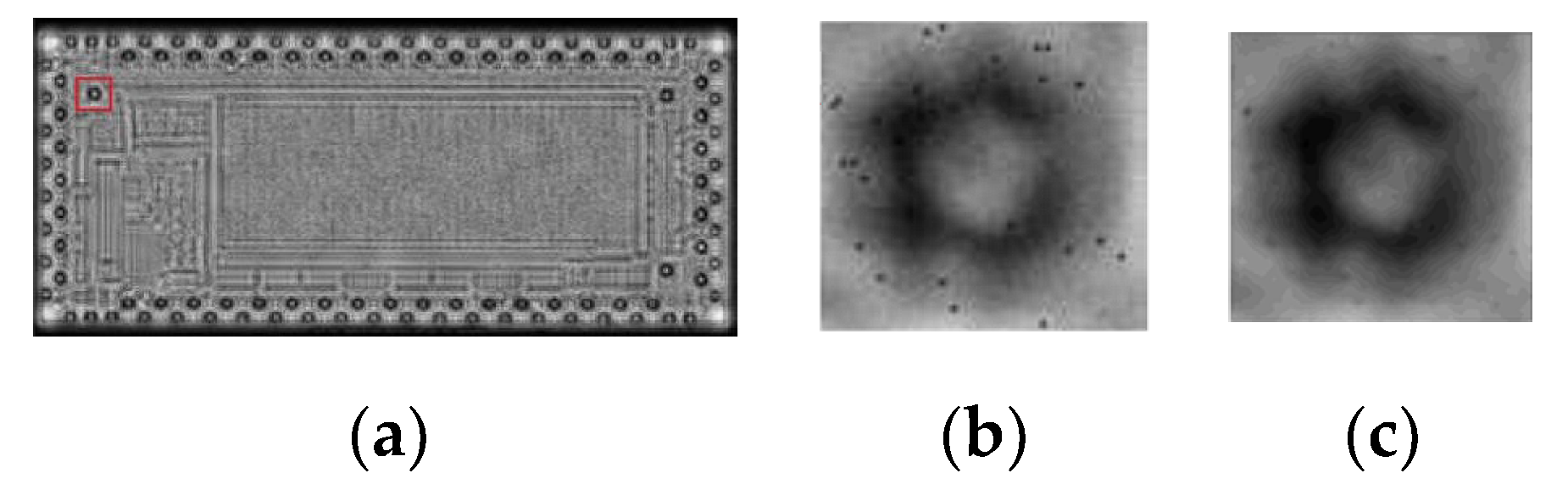
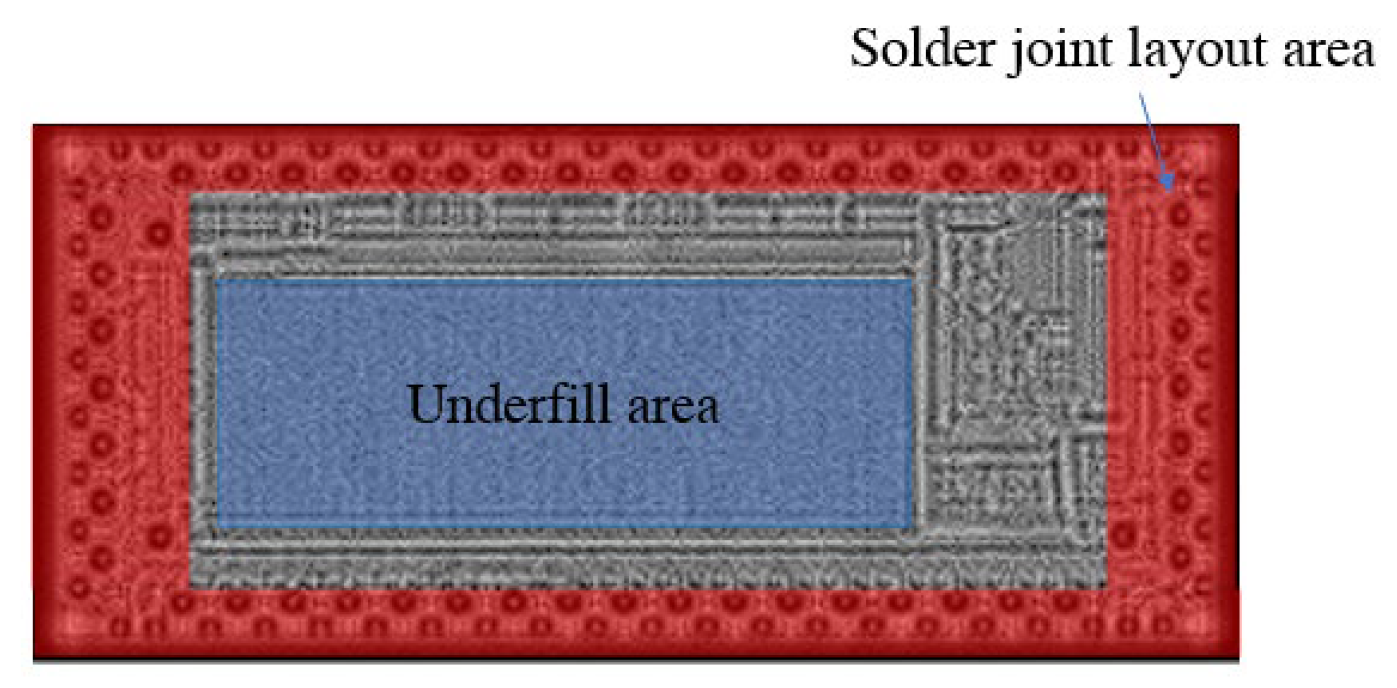
  • Experimental Data Acquisition: Four test boards were designed and manufactured, each equipped with 14 flip-chip packages mounted on a flame retardant type 4 substrate (FR-4). The boards underwent accelerated thermal cycling lifespan experiments until the chips detached. During the experiments, ultrasonic images of the flip chip were periodically acquired using the C-scan mode of an acoustic microscope, recording changes in their internal structure.
    To ensure the reliability and robustness of this study, a large-scale experimental dataset was collected. A total of 4 test boards were designed and fabricated, each equipped with 14 flip-chip packages, resulting in 56 flip chips for the experiments. Each test board contained 109 solder joints, and all samples underwent accelerated thermal cycling aging tests. During the experiment, data were collected every 4 thermal cycles, resulting in over 490 sampling points. The thermal cycling experiments lasted for a total of 2126 h over one year, producing more than 2 TB of experimental data. This dataset includes 3750 ultrasonic C-scan images of flip chips and over 400,000 solder joint images, providing a robust foundation for data analysis and model development.
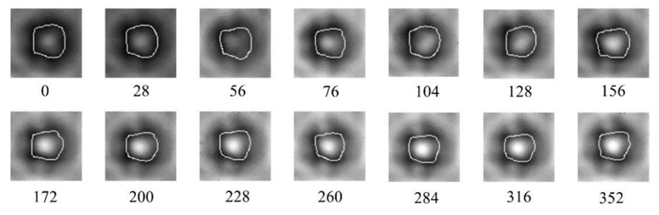
  • Ultrasonic Image Data Processing and Feature Extraction: The collected ultrasonic C-scan images were processed to ensure the consistency, stability, and accuracy of the image data. The mean intensity within the solder joint images was extracted as a key feature indicative of defects, which correlates with the solder joint’s fatigue stress and number of cycles, providing a basis for subsequent analysis.
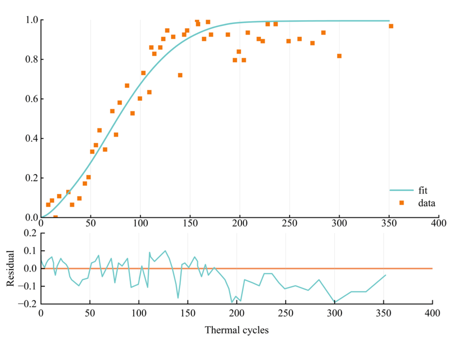
  • Failure Modeling and Lifespan Prediction: Based on the features of the solder joint images, a failure curve correlating the image features with the number of cycles was constructed. A cumulative failure probability model for individual solder joints was established using the Anderson–Darling test. This model was validated across multiple samples, demonstrating its accuracy and robustness in predicting the lifespan of solder joints. The model allows for the classification of solder joint health states, enabling lifespan prediction.

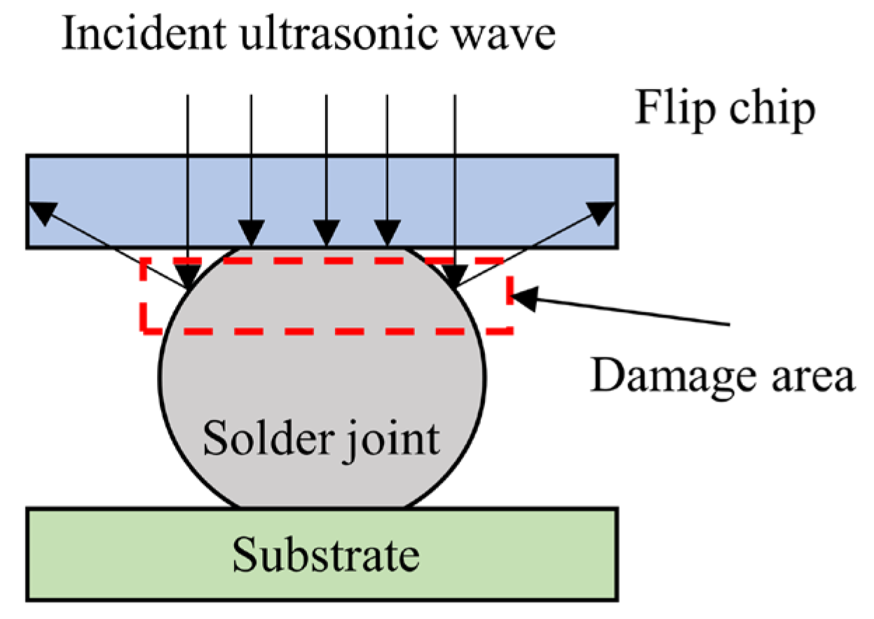
3. Ultrasonic Image Data Processing and Feature Extraction

To ensure that features extracted from ultrasonic images exhibit high consistency, stability, and accuracy, a series of image preprocessing methods for solder joints was implemented. These methods, as illustrated in Figure 2, address issues such as system noise, inconsistent dynamic range, overexposure, and defocus that may arise during the acoustic microimaging process. By applying these methods, the quality of the extracted data is significantly enhanced, facilitating more reliable and precise analyses.

3.1. Denoising of Flip-Chip Ultrasonic Image

Figure 3a presents a C-scan image of a flip chip captured using an acoustic microscope. A close examination of the solder joint in the magnified section shown in Figure 3b reveals the presence of “salt-and-pepper” noise caused by systematic errors, which significantly diminishes the detail in the image. To address this issue, a median filter with a 3 × 3 window and a stride of 1 was employed to remove the noise. Figure 3c displays the solder joint image after noise removal, demonstrating improved image clarity and detail.

3.2. Dynamic Normalization of Flip-Chip Ultrasonic Images

In acoustic microimaging, as the number of thermal cycling experiments increases, the degradation of solder joints leads to overexposure in the images. To optimize contrast, it is necessary to adjust the gain of the acoustic microscopy system. However, even with constant gain settings, differences in the dynamic range of images persist. Therefore, a method for normalizing the dynamic range of solder joint images is proposed, with the following steps.
Step 1. Data Acquisition and Extremum Determination:
Initiate by scanning all pixels in the original ultrasonic image, denoted as x . Extract the highest x m a x and lowest x m i n pixel values from this image.
Step 2. Dynamic Range Specification:
Define the original dynamic range R o as the difference between the maximum and minimum values identified in the image, calculated by R o = x m a x x m i n .
Step 3. New Dynamic Range Setting:
Set a new desired dynamic range Rn, typically 256 for standard 8-bit images. Calculate a midpoint value x m i d based on the original extremum values, defined as x m i d = x m i n + R o 2 .
Step 4. Intensity Adjustment:
Remap each pixel x i j in the original image using a normalized scaling function. This is achieved by first shifting the image intensities to a zero-based range, followed by scaling to the new range, and then recentering on the median. The transformation is defined by:
x i j = x i j x m i n R o R n + ( x m i d R n 2 )
where x i j is the adjusted pixel intensity.

3.3. Intensity Compensation of Flip-Chip Ultrasonic Images

In acoustic microscopy imaging of electronic packaging samples, continuous scanning and thermal cycling tests often induce minor positional deviations, leading to inevitable defocusing. Consequently, calibration and intensity compensation must be implemented to correct these defocus errors. Assuming the transducer is ideally focused, although solder joint degradation may alter the intensity of the image, the intensity within the central region of the flip chip’s C-scan images, indicated by the blue area in Figure 4 (where the coupling fluid is filled and the acoustic impedance remains constant), should remain stable. Therefore, the average intensity of this region was selected as a reference for intensity compensation across all flip-chip ultrasonic images.
First, calculate the mean intensity a i for the central region of each flip-chip image I ( x i , y i ) . This mean intensity measurement is essential, as it represents the typical intensity of the image’s central zone, which is less prone to peripheral distortions. Next, use the mean intensity a 0 from the central region of the flip-chip image obtained at cycle 0 of the accelerated thermal cycling experiment as the reference point. This reference intensity a 0 serves as the benchmark for assessing variations in subsequent images. Then, for each image, compute an intensity compensation value G i . This value is determined by subtracting the reference mean intensity a 0 from the mean intensity a i of each subsequent image. The computation is expressed as G i = a i a 0 . Finally, apply this compensation value G i to the corresponding image I ( x i , y i ) , resulting in an image I ( x i , y i ) that has been adjusted for intensity. This adjustment ensures uniformity in intensity across different imaging cycles.

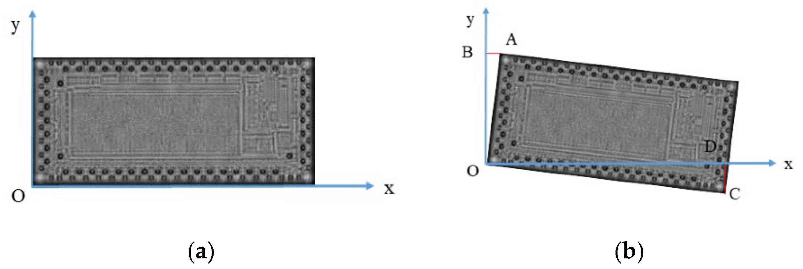
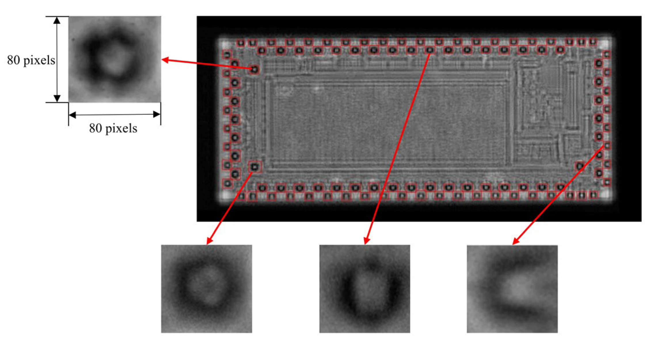
3.4. Flip-Chip Image Calibration and Solder Joint Image Segmentation

When using an ultrasonic microscopy imaging system to collect life-cycle data of flip chips, achieving ideal consistency is often challenging due to operational and environmental factors. Consequently, precise horizontal calibration of the images is required. Figure 5a depicts a perfectly aligned C-scan image of a flip chip. In this image, a Cartesian coordinate system is established with the origin at the lower-left corner, the bottom edge of the chip serving as the x-axis and the left edge as the y-axis. The horizontal calibration of the flip-chip image is performed accordingly.
The procedure begins with aligning the flip-chip image from Figure 5a, positioning its bottom-left endpoint at the origin of a Cartesian coordinate system. This alignment ensures the longer side of the chip image parallels the x-axis and the shorter side aligns with the y-axis. In Figure 5b, the angle α is defined at C O D , where point C has coordinates C ( x c , y c ) . A perpendicular line from point C to the x-axis intersects at point D , with coordinates D ( x c , 0 ) . The angle α is calculated by:
α = arccos ( x c x c 2 + y c 2 )
To finalize the calibration, the image is rotated by α degrees using Python’s rotation function (version 3.11.9), ensuring the chip image is horizontally aligned.
Given that the diameter of the solder joint is 140 μm and the system’s lateral resolution is 3 μm per pixel, the expected diameter of the solder joint image is approximately 47 pixels. To ensure complete coverage, images are captured using an 80 × 80 pixel window centered on the geometric center of the solder joint. Figure 6 presents the results from the collection of solder joints at different positions.

3.5. Feature Extraction of Solder Joint Image

The construction of the solder joint failure model relies on the mean intensity of the central region of solder joint images as a key degradation indicator. The central region is chosen for feature extraction based on the structural characteristics of flip-chip packaging, as illustrated in Figure 7. During thermal cycling experiments, solder joints experience thermal stress caused by mismatched thermal expansion between materials. This stress is particularly concentrated at the interfaces between the solder joints and adjacent materials, with the interface between the solder joint and the chip being especially prone to defects. Since the ultrasonic microimaging system collects data from directly above the solder joints, the most defect-prone area corresponds to the region within the black circular ring of the solder joint image. The black circular ring arises from the edge effect, where the spherical geometry of the solder joint scatters portions of the ultrasonic waves, leading to information loss. As a result, the real edges of the damaged regions are obscured within this black circular ring. Therefore, accurate identification of these concealed edges is critical for ensuring precise feature extraction.
In previous studies conducted by our group, it was observed that the real edges of the damaged regions hidden within the edge effect were closely associated with the local minima of grayscale values in the solder joint images [21]. By calculating the grayscale minima of each row and column, the real edges of the damaged regions can be accurately determined. This approach effectively addresses the challenges posed by the edge effect and ensures accurate feature extraction. Figure 8 illustrates the evolution of the damage region edges for the same solder joint throughout its complete life cycle obtained using this method. The numerical labels below the solder joint images correspond to the thermal cycling experiment periods.
To verify the effectiveness of the method used in this paper, a comparison with other edge detection techniques is presented in Figure 9. After thermal cycling experiments, some solder joints exhibit significant changes in the area, shape, and intensity of the central region due to material flow at elevated temperatures. In Figure 9, the leftmost column contains three solder joint images characterized by edge fractures, high noise, and distortion, respectively.
The detection results highlight the limitations of threshold-based edge detection methods, such as the Canny and Otsu algorithms [22,23]. In solder joint images, the grayscale variation within the dark ring is often subtle, making it challenging to select an appropriate threshold. A threshold that is too high results in edge information loss, leading to discontinuous edges, while a threshold that is too low introduces numerous false edges, compromising the accuracy of subsequent analysis. Gradient-based edge detection methods, such as the Prewitt operator [24], are highly sensitive to noise in the images that may originate from various sources such as equipment vibrations or electronic interference, significantly affecting local pixel intensities and causing the algorithm to erroneously detect nonexistent edges. Although filtering techniques can reduce noise to some extent, they often come at the cost of image detail, ultimately reducing the accuracy of edge detection. In contrast, the method used in this paper consistently delineates the damage regions with high precision, providing a robust foundation for failure feature extraction.
After determining the solder joint damage regions, data from over 400,000 solder joint images were selected for feature extraction. These images were obtained from 56 flip chips distributed across four sample boards, each containing 109 solder joints. For each solder joint image, the mean intensity of the damage region was computed, taking solder joint 107 from the second flip chip on sample board number 1 as an example, as shown in Figure 10.
Figure 11 presents the curve of mean intensity over the thermal cycling periods obtained by the proposed method. The blue curve represents the original, unprocessed data, the green curve corresponds to data after intensity compensation, and the brown curve represents data after comprehensive processing, including intensity compensation and dynamic range normalization. It can be observed that after a series of image processing steps, the extracted solder joint failure features evolve from initially disordered and irregular patterns to a trend that is positively correlated with the number of thermal cycling periods. This trend aligns with objective physical phenomena, laying a solid foundation for solder joint failure modeling and lifetime prediction.
In comparison, prior research [8] encountered significant challenges in accurately characterizing the solder joint failure process. The use of overly aggressive thermal cycling conditions caused samples to fail prematurely, resulting in an insufficient number of sampling points. Additionally, the image processing techniques employed lacked the capability to precisely delineate the boundaries of solder joint damage regions. By addressing these issues, the proposed method ensures robust sampling, employs accurate feature extraction, and enhances the reliability of results. These improvements enable the method to generate physically consistent and meaningful results that better capture solder joint failure features and support solder joint failure modeling and lifetime prediction.

4. Solder Joint Failure Modeling and Lifespan Prediction

4.1. Failure Modeling Based on Cumulative Failure Probability

The curves in Figure 11 represent the failure process of solder joint number 107 on the second flip chip of sample board number 1. To enable a more detailed quantitative analysis and lifespan prediction, it is necessary to convert these data into a mathematical expression. This study employed the Anderson–Darling (AD) test to determine the most suitable probability distribution that best describes the failure curve of the solder joint. Table 1 presents the results of the Anderson–Darling test. The results showed that with the exception of the two-parameter Weibull distribution, the p-values for the other distributions were less than 0.05 and the AD values were higher, indicating insufficient fit. The two-parameter Weibull distribution exhibits the highest degree of agreement with the experimental data.
Based on the conclusions derived from Table 1, a failure model for solder joint number 107 on the second flip chip of sample board number 1 has been developed, as illustrated in Figure 12. The probability density function (PDF) and cumulative distribution function (CDF) for the two-parameter Weibull distribution are defined as follows:
f ( t ) = k λ ( l i γ λ ) k 1 exp [ ( l i γ λ ) k ]
F ( t ) = 1 exp [ ( l i γ λ ) k ]
where i represents the failure time, k denotes the shape parameter, λ is the scale parameter, and γ represents the location parameter.
The results indicate that the parameter values for the model of solder joint number 107 on the second flip chip of sample board number 1 are k = 1.24 ,   λ = 74.61 and γ = 0 . Consequently, the cumulative failure probability model for this solder joint based on the two-parameter Weibull distribution is:
F ( t ) = 1 exp [ ( t i 74.61 ) 1.24 ]
The model provides a precise mathematical description of the entire service lifespan-to-failure process of solder joint number 107 on the second flip chip of sample board number 1. However, it currently applies only to this specific solder joint, and therefore further validation of its generalizability is required to extend its applicability.

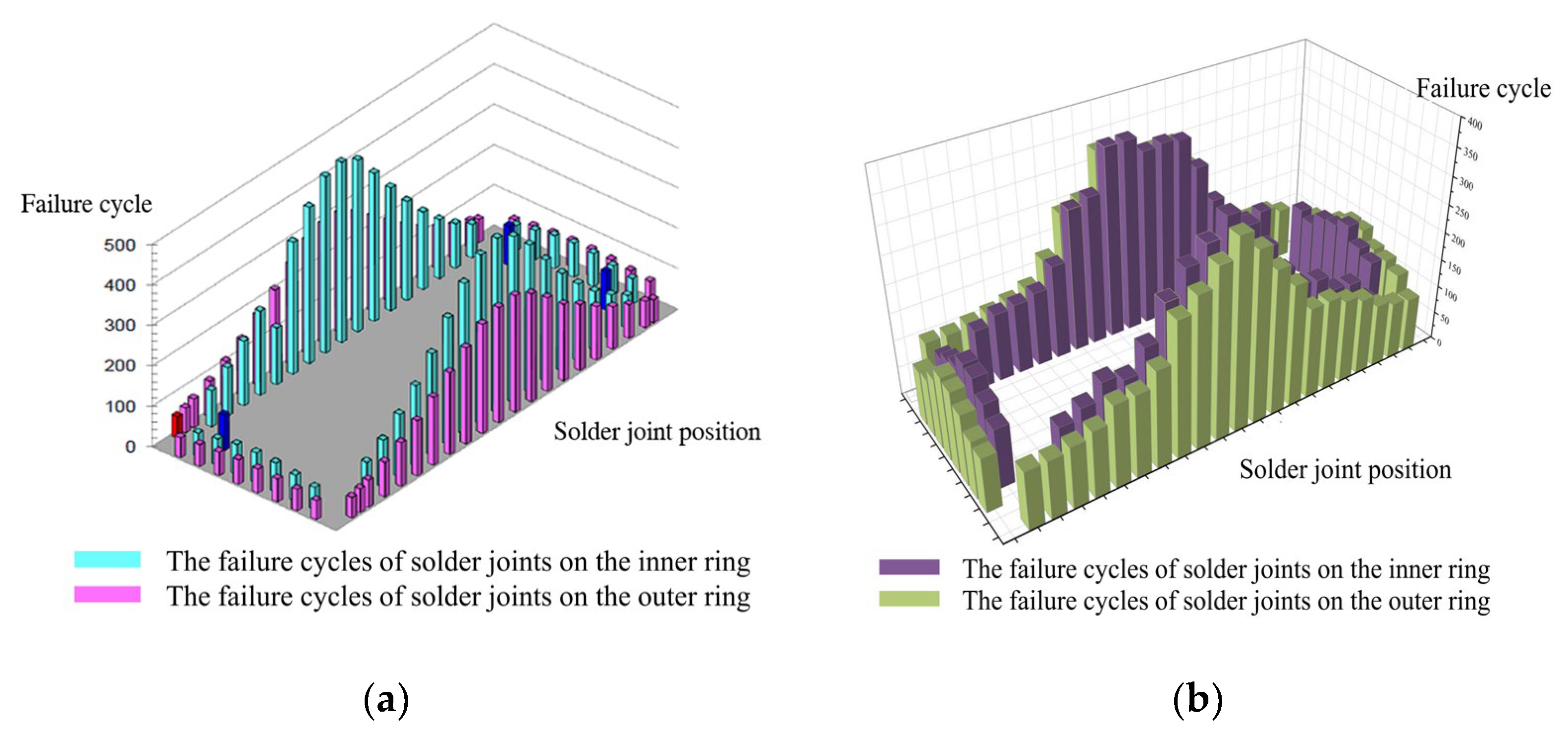
4.2. Validation of Solder Joint Failure Model Based on Positional Differences

To validate the adaptability of the model when addressing different solder joint locations on flip chips, image data from four solder joints located in various positions, solder joint 4 (inner circle), solder joint 42 (outer circle), and solder joints 69 and 102 (the corners of the chip) were selected as samples for validation. The validation results are shown in Figure 13. The results indicate a high degree of fit between the failure curves of the solder joints and the cumulative failure model based on the two-parameter Weibull distribution. Although there are differences in the shape of the curves, primarily reflected in the failure rates and start and end times, all samples typically underwent a process of no defects, defect initiation, and final failure.
To further analyze the differences in behavior at various stages, precise failure model parameters were calculated for the four solder joints and are summarized in Table 2. The combination of the failure curves in Figure 13 and the cumulative failure model parameters in Table 2 demonstrates the variability in the parameters of the two-parameter Weibull distribution model for solder joints at different locations. The failure shape parameter is consistently near 1.3 for all joints, indicating uniformity in the statistical distribution shape and suggesting that the failure mechanisms are fundamentally the same. However, the failure time parameter shows clear position dependence, reflecting the variance in aging rates due to differences in stress and thermal cycling at different locations. This finding is crucial for understanding the reliability of solder joints and directly relates to the performance stability and lifespan prediction of the chip under varying environmental conditions.
After processing the entire life-cycle ultrasonic images of all solder joints as described above, the model’s performance was evaluated using the maximum absolute value of the fitting residuals e i as the metric. The formula for calculating the maximum absolute value of fitting residuals is:
| e i | = max ( | y i F ( t i ) | )
where y i represents the actual observed value and F ( t i ) is the model’s predicted value. The results computed for all chips on four experimental sample boards are shown in Table 3.
The results in Table 3 demonstrate that when fitting the solder joint data of flip chips using the two-parameter Weibull distribution cumulative failure model, the absolute value of the residuals | e i | does not exceed 0.24 on any of the experimental sample boards. This consistency in handling data from different samples underscores the model’s reliability and universality in practical applications.

4.3. Solder Joint Lifespan Prediction

In the actual aging process of solder joints, due to their varied positions on the chip, the extent of stress and thermal cycling impact differs, leading to variations in aging rates. These differences are primarily manifested in two ways: the rate of progression of solder joint failure and the timing of the failure’s onset and termination. The failure timing not only serves as a critical indicator for determining the stages of defect-free, defect initiation, and defect-caused failure but also as a crucial basis for lifespan prediction.
The failure curve of solder joint number 107 on the second flip chip of sample board number 1 reveals that during accelerated thermal cycling life tests, the intensity of the damaged area of the solder joint significantly increases around the 50th cycle, the rate of increase slows down after about 130 cycles, and it stabilizes after 150 cycles. To precisely define the failure process, the inflection points of the curve are determined using the second derivative, identified as the initial failure point A and the termination point B.
The second derivative of the cumulative failure model F t based on the two-parameter Weibull distribution, F t , is:
F ( t ) = k λ [ ( k 1 ) ( t γ λ ) k 2 1 λ exp [ ( t γ λ ) k ] k ( t γ λ ) 2 k 2 1 λ exp [ ( t γ λ ) k ] ]
By setting F t = 0 , we identified two temporal inflection points, A and B, on the failure curve, as shown in Figure 14b. Points A and B are defined as the initiation and termination points of solder joint failure, respectively, then the health status of the solder joint is classified into the following three stages.
1.
Healthy and Defect-Free Solder Joint Stage (from cycle 0 to cycle A of the accelerated thermal cycling test):
During this phase, the solder joint exhibits excellent mechanical and thermal properties, with no visible or functional defects. The structure and material properties of the solder joint remain in their initial state, fully meeting design and functional requirements. The reliability of the solder joint in this stage is exceptionally high.
2.
Defective but Non-Failure Solder Joint Stage (from cycle A to cycle B of the accelerated thermal cycling test):
As the number of test cycles increases, the solder joint begins to show signs of structural fatigue or material degradation. Although these initial defects do not yet lead to a complete loss of function, they do impact performance, evidenced by increased electrical resistance or decreased thermal conductivity. While the solder joint can still meet basic operational requirements, its performance stability and long-term reliability begin to be compromised.
3.
Failed Solder Joint Stage (after cycle B of the accelerated thermal cycling test):
Once the test cycles exceed point B, the performance of the solder joint significantly deteriorates, failing to meet the minimum design standards and marking the entrance into a failure state. At this point, the physical and chemical properties of the solder joint may have undergone irreversible changes, such as crack propagation or poor contact, resulting in the loss of its original function.
In the assessment of solder joint lifespan, point B is defined as the critical time node for solder joint failure. This node marks a significant decline in solder joint performance to a state where it no longer meets the minimum design standards. By monitoring the degradation process of solder joints in accelerated thermal cycling tests, the solder joint is considered to have exhausted its lifespan upon reaching point B. Based on the remaining lifespan data of solder joints at different positions on the chip, effective prediction of the overall lifespan of electronic packaging is achievable.

4.4. Simulation Validation

The lifespan of all solder joints on the second flip chip of sample board number 1 was calculated and visually displayed in three dimensions. These results were then compared with those of finite element simulations, as shown in Figure 15.
Figure 15a presents the lifespan predictions for each solder joint on the second flip chip of sample board number 1 using finite element simulation techniques. The failure cycles of solder joints on the inner ring are marked in cyan, while those on the outer ring are marked in purple, the solder joint No.1 on the chip is marked in red, and three special solder joints in the central region are marked in blue. Clearly demonstrating a trend of decreasing quality with an increasing number of thermal cycling tests. The simulation data reveal that solder joints located at the center of the inner ring exhibit longer lifespans, capable of withstanding approximately 400 thermal cycling tests, whereas those at the corners of the outer ring show shorter lifespans, enduring only about 100 cycles. The lifespan of the solder joints is represented in a normal distribution.
Figure 15b displays the solder joint lifespan results obtained using the method proposed in this paper. The failure cycles of solder joints on the inner ring are represented in purple, while those on the outer ring are shown in green. Due to the multiaxial stress endured by the solder joints during the thermal cycling tests, the actual lifespans are slightly less than those predicted by the simulations. The method reveals that solder joints in the inner ring tend to have longer lifespans compared to those in the outer ring, and this finding aligns closely with the lifespan distribution trends observed in the simulation results. The conclusions derived from this method provide significant guidance for understanding the characteristics of solder joint lifespan and influencing factors, offering substantial data support and theoretical basis for further in-depth research.

5. Discussion of Results

The ultrasonic microimaging methodology demonstrates non-destructive monitoring capability for solder joint degradation, overcoming the inherent limitations of conventional destructive cross-sectioning methods. Through systematic implementation of denoising, normalization, and intensity compensation algorithms, the image processing pipeline effectively enhanced signal integrity, enabling precise tracking of defect evolution from initiation to complete failure.
The extracted mean intensity of solder joint central regions exhibited a strong correlation with thermal cycling progression, serving as a quantifiable degradation indicator. This metric successfully captured the three-stage failure process: initial stability, gradual defect accumulation, and final abrupt failure. Position-dependent lifespan variations were clearly observed, with corner joints showing significantly shorter service life compared to central joints, consistent with the anticipated thermal stress distribution patterns in electronic packaging.
The two-parameter Weibull distribution model provides a statistically robust framework for failure probability estimation, as evidenced by the low residual errors between experimental data and model predictions. This mathematical approach effectively differentiates failure characteristics across solder joint locations while maintaining computational efficiency.
While the method demonstrates strong experiment–model consistency, its current implementation focuses on steady-state thermal cycling conditions. Further validation is required for transient thermal shock scenarios and multi-axial mechanical loading environments. The image resolution threshold (exact value specified in original data) may also limit detection of sub-micron scale early-stage defects.

6. Conclusions

This study developed and validated a non-destructive lifespan prediction method for electronic packaging based on ultrasonic microimaging technology. Through advanced image processing and failure modeling, the study addressed key challenges in solder joint reliability assessment. The conclusions of this study are as follows.
(1)
A novel non-destructive approach was established to monitor solder joint degradation throughout the life cycle, overcoming the limitations of conventional destructive methods and enabling continuous data collection under accelerated thermal cycling conditions.
(2)
The propagation mechanisms of ultrasound in electronic packaging were analyzed, establishing a quantitative relationship between ultrasonic image intensity and internal defects. This innovation enables precise tracking of defect evolution and bridges imaging data with failure mechanisms.
(3)
Image processing techniques, including denoising, normalization, and intensity compensation, were enhanced to address system noise, overexposure, and defocusing. These improvements significantly increased data quality, ensuring reliable feature extraction for failure modeling.
(4)
A robust failure model based on cumulative failure probability was developed, effectively capturing position-dependent failure behaviors. This model accurately predicts solder joint lifespans and resolves challenges related to stress concentration and thermal gradient effects.
(5)
Validation through extensive experimental data and comparison with simulation results confirmed the accuracy and reliability of the proposed method, demonstrating its potential for practical application in reliability assessment and predictive maintenance.

Author Contributions

Conceptualization, H.M. and G.Z.; Methodology, H.M. and G.Z.; Software, H.W.; Validation, H.W.; Formal analysis, H.W.; Investigation, H.M. and G.Z.; Resources, H.M. and G.Z.; Data curation, H.W.; Writing—original draft, H.W.; Writing—review & editing, H.M., G.Z., Y.C. and M.D.; Visualization, H.W.; Supervision, H.M., G.Z. and Y.C.; Project administration, H.M., G.Z. and M.D.; Funding acquisition, H.M. and G.Z. All authors have read and agreed to the published version of the manuscript.

Funding

This research was funded by National Key R&D Program of China (grant number 2022YFF0605300). National Natural Science Foundation of China (grant number 61674121), Newton Fund (grant number 332397914), and the EU H2020-Marie Sklodowska-Curie research and innovation staff exchange 2019 grant (No. 871163).

Institutional Review Board Statement

Not applicable.

Informed Consent Statement

Not applicable.

Data Availability Statement

The original contributions presented in this study are included in the article. Further inquiries can be directed to the corresponding author.

Conflicts of Interest

The authors declare no conflict of interest.

References

  1. Huang, Y.; Deng, H.; Luo, Y.; Xiao, F.; Liu, B.; Tang, X. Fatigue mechanism of die-attach joints in IGBTs under low-amplitude temperature swings based on 3D electro-thermal-mechanical FE simulations. IEEE Trans. Ind. Electron. 2020, 68, 3033–3043. [Google Scholar] [CrossRef]
  2. Li, Y.; He, J.; Won, D.; Yoon, S.W. Noncontact reflow oven thermal profile prediction based on artificial neural network. IEEE Trans. Compon. Packag. Manuf. Technol. 2021, 11, 2229–2237. [Google Scholar] [CrossRef]
  3. Honarvar, S.; Nourani, A.; Karimi, M. Effect of thermal treatment on fracture behavior of solder joints at various strain rates: Comparison of cyclic and constant temperature. Eng. Fail. Anal. 2021, 128, 105636. [Google Scholar] [CrossRef]
  4. Li, L.; Du, X.; Chen, J.; Wu, Y. Thermal fatigue failure of micro-solder joints in electronic packaging devices: A review. Materials 2024, 17, 2365. [Google Scholar] [CrossRef]
  5. Akkara, F.J.; Hamasha, S.D.; Alahmer, A.; Evans, J.; Belhadi, M.E.; Wei, X. The effect of micro-alloying and surface finishes on the thermal cycling reliability of doped SAC solder alloys. Materials 2022, 15, 6759. [Google Scholar] [CrossRef] [PubMed]
  6. Sha, Y.; He, Z.; Gutierrez, H.; Du, J.; Yang, W.; Lu, X. The intelligent detection method for flip chips using CBN-S-Net algorithm with SAM images. J. Manuf. Process. 2022, 83, 60–67. [Google Scholar] [CrossRef]
  7. Lu, X.; Liu, F.; He, Z.; Li, L.; Hu, N.; Su, L. Defect inspection of flip chip package using SAM technology and fuzzy C-means algorithm. Sci. China Technol. Sci. 2018, 61, 1426–1430. [Google Scholar] [CrossRef]
  8. Yang, R.S.; Braden, D.R.; Zhang, G.M.; Harvey, D.M. Through lifetime monitoring of solder joints using acoustic micro imaging. Solder. Surf. Mt. Technol. 2012, 24, 30–37. [Google Scholar] [CrossRef]
  9. Yang, R.S.; Braden, D.R.; Zhang, G.-M.; Harvey, D.M. An automated ultrasonic inspection approach for flip chip solder joint assessment. Microelectron. Reliab. 2012, 52, 2995–3001. [Google Scholar] [CrossRef]
  10. Wang, Y.; Yu, S.; Li, J. The Temperature Cycling Characteristic of Copper Pillar Solder Joints. IEEE Trans. Compon. Packag. Manuf. Technol. 2024, 14, 1043–1050. [Google Scholar] [CrossRef]
  11. Lederer, M.; Kotas, A.B.; Khatibi, G. Lifetime modeling of solder joints based on accelerated mechanical testing and finite element analysis. Power Electron. Devices Compon. 2023, 4, 100034. [Google Scholar] [CrossRef]
  12. Sun, F.Q.; Liu, J.C.; Cao, Z.Q.; Li, X.Y.; Jiang, T.M. Modified Norris–Landzberg model and optimum design of temperature cycling alt. Strength Mater. 2016, 48, 135–145. [Google Scholar] [CrossRef]
  13. Haq, M.A.; Hoque, M.A.; Suhling, J.C.; Lall, P. Determination of Anand Parameters from Creep Testing of SAC305 Solder Joints. In Proceedings of the International Electronic Packaging Technical Conference and Exhibition 2020, Virtual, 27–29 October 2020; American Society of Mechanical Engineers: New York, NY, USA, 2020; Volume 84041, p. V001T01A016. [Google Scholar]
  14. Samavatian, V.; Iman-Eini, H.; Avenas, Y.; Samavatian, M. Effects of creep failure mechanisms on thermomechanical reliability of solder joints in power semiconductors. IEEE Trans. Power Electron. 2020, 35, 8956–8964. [Google Scholar] [CrossRef]
  15. Prisacaru, A.; Gromala, P.J.; Han, B.; Zhang, G.Q. Degradation estimation and prediction of electronic packages using data-driven approach. IEEE Trans. Ind. Electron. 2021, 69, 2996–3006. [Google Scholar] [CrossRef]
  16. Goebel, K.; Rajamani, R. Policy, regulations and standards in prognostics and health management. Int. J. Progn. Health Manag. 2021, 12, 1–16. [Google Scholar] [CrossRef]
  17. Depiver, J.A.; Mallik, S.; Amalu, E.H. Thermal fatigue life of ball grid array (BGA) solder joints made from different alloy compositions. Eng. Fail. Anal. 2021, 125, 105447. [Google Scholar] [CrossRef]
  18. Xia, J.; Li, G.; Li, B.; Cheng, L.; Zhou, B. Fatigue life prediction of package-on-package stacking assembly under random vibration loading. Microelectron. Reliab. 2017, 71, 111–118. [Google Scholar] [CrossRef]
  19. Watanabe, Y.; Yamaguchi, H.; Enomoto, T.; Ogawa, K.; Kobayashi, T.; Omiya, M. Evaluation of thermal fatigue crack propagation in underfill resin materials for electronic packages. Fatigue Fract. Eng. Mater. Struct. 2022, 45, 1349–1360. [Google Scholar] [CrossRef]
  20. Santos, M.; Santos, J.; Reis, P.; Amaro, A. Ultrasonic C-scan techniques for the evaluation of impact damage in CFRP. Mater. Test. 2021, 63, 131–137. [Google Scholar] [CrossRef]
  21. Lee, C.S.; Zhang, G.M.; Harvey, D.M.; Ma, H.W. Development of C-Line plot technique for the characterization of edge effects in acoustic imaging: A case study using flip chip package geometry. Microelectron. Reliab. 2015, 55, 2762–2768. [Google Scholar] [CrossRef]
  22. Fang, T.; An, J.; Chen, Q.; He, Y.; Wang, H.; Zhang, X. Progress and comparison in nondestructive detection, imaging and recognition technology for defects of wafers, chips and solder joints. Nondestruct. Test. Eval. 2024, 39, 1599–1654. [Google Scholar] [CrossRef]
  23. Yan, H.; Liu, L.; Chen, Z.; Mo, J.; Liu, J. An Adaptive Contour Extraction Algorithm for Circular Solder Joints in PCBA of Smart Phone. J. Comput. -Aided Des. Comput. Graph. 2023, 35, 405–412. [Google Scholar]
  24. Zhang, Y.; Wang, Z.; Wang, Y.; Zhang, C.; Zhao, B. Research on image defect detection of silicon panel based on prewitt and canny operator. Front. Phys. 2021, 9, 701462. [Google Scholar] [CrossRef]
Figure 1. Schematic diagram of lifespan prediction method using ultrasonic microimaging for electronic packaging.
Applsci 15 03246 g001
Figure 2. Schematic diagram of data processing method for solder joint images.
Applsci 15 03246 g002
Figure 3. Result of median filtering denoising on flip-chip and solder joint images. (a) Flip-chip C-scan image; (b) original image of solder joint with noise, derived from the solder joint marked by the red box in (a); (c) denoising results using 3 × 3, step size 1 square window.
Applsci 15 03246 g003
Figure 4. Schematic diagram of intensity compensation method for flip-chip images.
Applsci 15 03246 g004
Figure 5. Schematic diagram of image calibration for flip chips. (a) Perfectly horizontally calibrated flip-chip image; (b) uncalibrated flip-chip image. A and C are the top-left and bottom-right corners of the flip chip, respectively. B and D are the projections of A and C on the y- and x-axes.
Applsci 15 03246 g005
Figure 6. Segmentation results of solder joint images at different locations.
Applsci 15 03246 g006
Figure 7. Schematic diagram of flip-chip package structure.
Applsci 15 03246 g007
Figure 8. Damage Area edge extraction of the same solder joint at different cycles of thermal cycling test.
Applsci 15 03246 g008
Figure 9. Comparison of edge detection results for solder joint damage areas.
Applsci 15 03246 g009
Figure 10. Ultrasonic image of solder joint 107 on flip chip 2 of experimental sample 1.
Applsci 15 03246 g010
Figure 11. Failure curve of solder joint 107 on flip chip 2 of experimental sample 1 using proposed method.
Applsci 15 03246 g011
Figure 12. Fitting result of failure data for solder joint 107 on flip chip 2 of experimental sample 1.
Applsci 15 03246 g012
Figure 13. Fitting results of failure models for solder joints at different locations on chip 2, sample 1. (a) Solder joint 4; (b) solder joint 42; (c) solder joint 69; (d) solder joint 102.
Applsci 15 03246 g013
Figure 14. Determination of failure time for solder joint 107 on flip chip 2 of sample 1. (a) Solder joint failure curve; (b) initial failure point A and termination point B.
Applsci 15 03246 g014
Figure 15. Comparison of lifespan prediction effectiveness for solder joints. (a) Simulation results of solder joint lifespan; (b) solder joint lifespan according to the method proposed in this paper.
Applsci 15 03246 g015
Table 1. Results of Anderson–Darling test.
Distribution FunctionADp
Normal3.416<0.005
Exponential normal6.402<0.005
Index7.043<0.003
Weibull5.212<0.010
3-parameter Weibull2.790<0.005
Gamma5.451<0.005
Logistic3.087<0.005
2-parameter Weibull cumulative0.9870.526
Table 2. Fitting parameters of failure models for solder joints at different locations in Figure 13.
Solder Joint on Flip Chip 2 of Sample 1 Scale   Parameter   λ Shape   Parameter   k
Solder joint 474.221.24
Solder joint 4281.181.26
Solder joint 6984.451.27
Solder joint 10287.651.34
Table 3. Maximum absolute values of fitting residuals | e i | for various experimental samples.
Test Sample Number Maximum   Absolute   Value   of   Fitting   Residuals   | e i |
Sample 10.23
Sample 20.24
Sample 30.20
Sample 40.20
Disclaimer/Publisher’s Note: The statements, opinions and data contained in all publications are solely those of the individual author(s) and contributor(s) and not of MDPI and/or the editor(s). MDPI and/or the editor(s) disclaim responsibility for any injury to people or property resulting from any ideas, methods, instructions or products referred to in the content.

