Article

Tuning Optical Performance of Silicon Solar Cells with Micro-Structured Multilayer Antireflection Coatings

by
Ibrahim H. Khawaji
1,2,3,*,
Ala H. Sabeeh
1,2,3,
Tawfik Ismail
2,3 and
Basma E. Abu-Elmaaty
3,4
1
Department of Electrical Engineering, Taibah University, Medina P.O. Box 344, Saudi Arabia
2
Department of Telecommunication Engineering, Taibah University, Medina P.O. Box 344, Saudi Arabia
3
Energy, Industry and Advanced Technologies Research Center, Taibah University, Medina P.O. Box 344, Saudi Arabia
4
Department of Electronics and Electrical Communications Engineering, Faculty of Engineering, Tanta University, Tanta P.O. Box 31527, Egypt
*
Author to whom correspondence should be addressed.
Appl. Sci. 2025, 15(6), 3053; https://doi.org/10.3390/app15063053
Submission received: 17 January 2025 / Revised: 17 February 2025 / Accepted: 23 February 2025 / Published: 12 March 2025

Abstract

:
This study investigates the potential of patterned multiple-layer anti-reflection coatings (MLARCs) integrated with nanocrystalline quantum dots (NQDs) to enhance silicon solar cell (Si-SC) performance by significantly reducing reflection losses. Through a combination of experimental characterization and numerical modeling, the impact of single-layer (SLARCs), continuous MLARCs, and patterned MLARCs on optical and electrical properties was assessed. The results demonstrate substantial improvements in light trapping and absorption through the implementation of patterned MLARCs.

1. Introduction

Silicon-based solar cells (Si-SCs) remain the dominant technology in the photovoltaic industry, despite their theoretical efficiency limitations imposed by the Shockley–Queisser limit. While substantial progress has been made in achieving commercial efficiencies approaching 29% under standard test conditions (STCs), significant performance losses persist due to a combination of factors, including optical reflection, thermalization, and recombination losses [1,2].
A substantial portion of incident solar radiation is reflected at the air–silicon interface owing to the mismatch in refractive indices. This reflection loss, typically around 35%, significantly reduces the overall efficiency of Si-SCs. To mitigate these losses, various anti-reflection coating (ARC) strategies, such as surface texturing, single-layer ARCs (SLARCs), and multi-layer ARCs (MLARCs), have been implemented [3,4,5,6]. However, the inefficient absorption of ultraviolet (UV) radiation by silicon, leading to approximately 10% energy loss, necessitates additional approaches to broaden the spectral response of Si-SCs [7,8,9].
Traditional ARCs, such as SiO2 and Si3N4, have been widely employed to enhance light absorption and minimize reflection in Si-SCs. These materials offer compatibility with standard fabrication processes, cost-effectiveness, and proven performance across a broad spectral range. To further augment light absorption, nanocrystalline quantum dots (NQDs) have emerged as promising candidates. By downshifting high-energy photons to wavelengths more efficiently absorbed by silicon, NQDs can broaden the spectral response of Si-SCs [10,11,12]. However, the stability and durability of NQDs under environmental conditions necessitate protective measures. Lithium fluoride (LiF), with its high transparency and passivation properties, serves as an ideal encapsulation layer for NQDs, ensuring their long-term performance and stability [13,14].
Building upon these advancements, the integration of micro-/nano-patterned structures within MLARCs offers a promising avenue for further enhancing light management and device performance. By precisely controlling the dimensions and distribution of these patterns, it is possible to optimize light trapping and reduce reflection losses, leading to improved solar cell efficiency [13,14].
To address these challenges and enhance light absorption in Si-SCs, this study investigates the potential of patterned MLARCs integrated with NQDs to enhance Si-SC performance by significantly reducing reflection losses. By combining experimental characterization and numerical modeling, we aim to optimize the design and performance of these structures. The incorporation of NQDs within the MLARCs offers the potential to improve UV light absorption through downshifting while enhancing light trapping through the creation of intricate patterns. By carefully optimizing ARC design, material selection, and device configuration, this research seeks to achieve substantial improvements in the overall efficiency of silicon solar cells.

2. Proposed Device Structures

To investigate the influence of SLARCs and MLARCs on Si-SC performance, various device configurations are constructed utilizing the selected materials (SiO2, Si3N4, NQDs, and LiF). The SLARC-based Si-SC comprises four distinct configurations featuring continuous thin films, as illustrated in Figure 1a. For MLARC-based Si-SCs, two primary configurations are explored: continuous and micro-/nano-patterned structures, as depicted in Figure 1b. Within the MLARC category, four specific designs are implemented: a continuous MLARC with a SiO2/NQDs/LiF stack (b1), a continuous MLARC with a Si3N4/NQDs/LiF stack (b2), a patterned MLARC with a SiO2/NQDs/LiF configuration (b3), and a patterned MLARC with a Si3N4/NQDs/LiF configuration (b4).

3. Experimental Procedure

This study commenced with a thorough optical characterization of SiO2- and Si3N4-based SLARCs. To achieve this, a series of 18 SLARC samples were fabricated by depositing thin films of each material onto n-type (100) silicon wafers with a resistivity of less than 0.003 ohms-cm, doped with arsenic.
SiO2 SLARCs were produced through thermal oxidation at 1100 °C, resulting in thicknesses of 90, 120, and 150 nm (three samples for each thickness). Precise thickness measurements were obtained using a reflectometer, yielding values of 98.1 ± 0.3 nm, 129.6 ± 0.3 nm, and 147.0 ± 0.4 nm, respectively. Conversely, Si3N4 SLARCs were fabricated via plasma-enhanced chemical vapor deposition at 770 °C and 250 mTorr, targeting thicknesses of 90, 120, and 150 nm (three samples for each thickness). The measured thicknesses for these samples were 92.5 ± 1.1 nm, 117.6 ± 1.3 nm, and 145.7 ± 1.5 nm.
The optical properties of the SLARCs were determined by measuring reflectivity and refractive index using a UV-VIS spectrophotometer and ellipsometer over a spectral range of 350 to 1000 nm. To complete the optical characterization, the optical properties of NQDs and LiF films, essential components for subsequent MLARC configurations, were sourced from previous studies [13,14]. Notably, NQDs (CdSe/ZnS) were integrated into SLARCs via a mist deposition technique, while LiF was incorporated through thermal evaporation. The optical properties of the silicon substrate were referenced from Green and Keevers [15,16].
Building upon the experimentally measured optical properties of SLARCs, the second phase of the study involved integrating both SLARCs and MLARCs (SiO2/NQDs/LiF and Si3N4/NQDs/LiF) into Si-SCs. To gain insight into light propagation and interaction within these complex structures, both continuous and patterned MLARC configurations were subjected to rigorous modeling and simulation using Ansys-Lumerical FDTD software.
A comprehensive analysis of the simulated structures yielded valuable optical and electrical properties, including optical reflectivity, internal and external quantum efficiencies, open-circuit voltage, short-circuit current, fill factor, and ultimately, power conversion efficiency.

4. Experimental Characterization of Si-SC Structures with SLARC

The performance of a single-layer anti-reflection coating (SLARC) is critically influenced by its refractive index (n) and thickness (d). Optimal SLARC design necessitates a refractive index that is the geometric mean of air ( n 0 1 ) and silicon ( n S i 3.5 ) for the visible spectrum. Theoretically, the ideal SLARC thickness is a quarter-wavelength ( λ ) of the target light, as expressed below:
d = λ 4 n
However, achieving optimal performance across the entire solar spectrum often requires deviations from this theoretical thickness. To this end, a comprehensive analysis of refractive index and optical reflectivity was conducted for SiO2 and Si3N4 SLARCs with varying thicknesses across the wavelength range of 350 nm to 1000 nm. These measurements provide essential insights into the relationship between SLARC properties and their impact on solar cell performance.

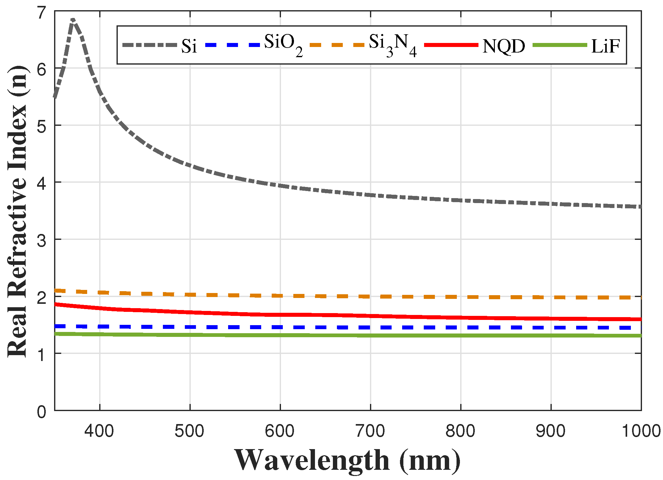
4.1. Refractive Index Characteristics

The refractive index of a thin film is influenced by factors such as wavelength, temperature, and material purity. While these parameters can induce variations, standardized refractive index values are commonly employed at a reference wavelength of approximately 550 nm. Representative refractive indices at this wavelength are 3.5 for Si, 1.45 for SiO2, 2.0 to 2.2 for Si3N4 (dependent on composition), 1.39 for LiF, and 1.5 to 2.5 for CdSe/ZnS NQDs (varying with quantum dot characteristics) [17,18,19].
To characterize the wavelength-dependent refractive index behavior, single-layer thin films of SiO2, Si3N4, CdSe/ZnS NQDs, and LiF were deposited on n-type Si wafers. The refractive index of silicon was referenced from Green and Keevers [15,16]. For single-layer thin films, the refractive index was measured over a spectral range of 350 to 1000 nm. Figure 2 presents the measured refractive index as a function of wavelength for each single-layer thin film.
The results indicate relatively stable refractive index values for all materials across the solar spectrum (approximately 350 to 1000 nm). At a wavelength of 550 nm, the refractive indices for SiO2, Si3N4, CdSe/ZnS NQDs, and LiF thin films were determined to be 1.46, 2.01, 1.67, and 1.32, respectively. Applying the quarter-wave thickness condition for optimal anti-reflection performance yielded estimated thicknesses of 101, 73, 46, and 112 nm for SiO2, Si3N4, CdSe/ZnS NQDs, and LiF thin films, respectively. These calculated thicknesses served as a foundation for the design of both continuous and patterned MLARC and SLARC structures, specifically SiO2/NQD/LiF and Si3N4/NQD/LiF configurations.

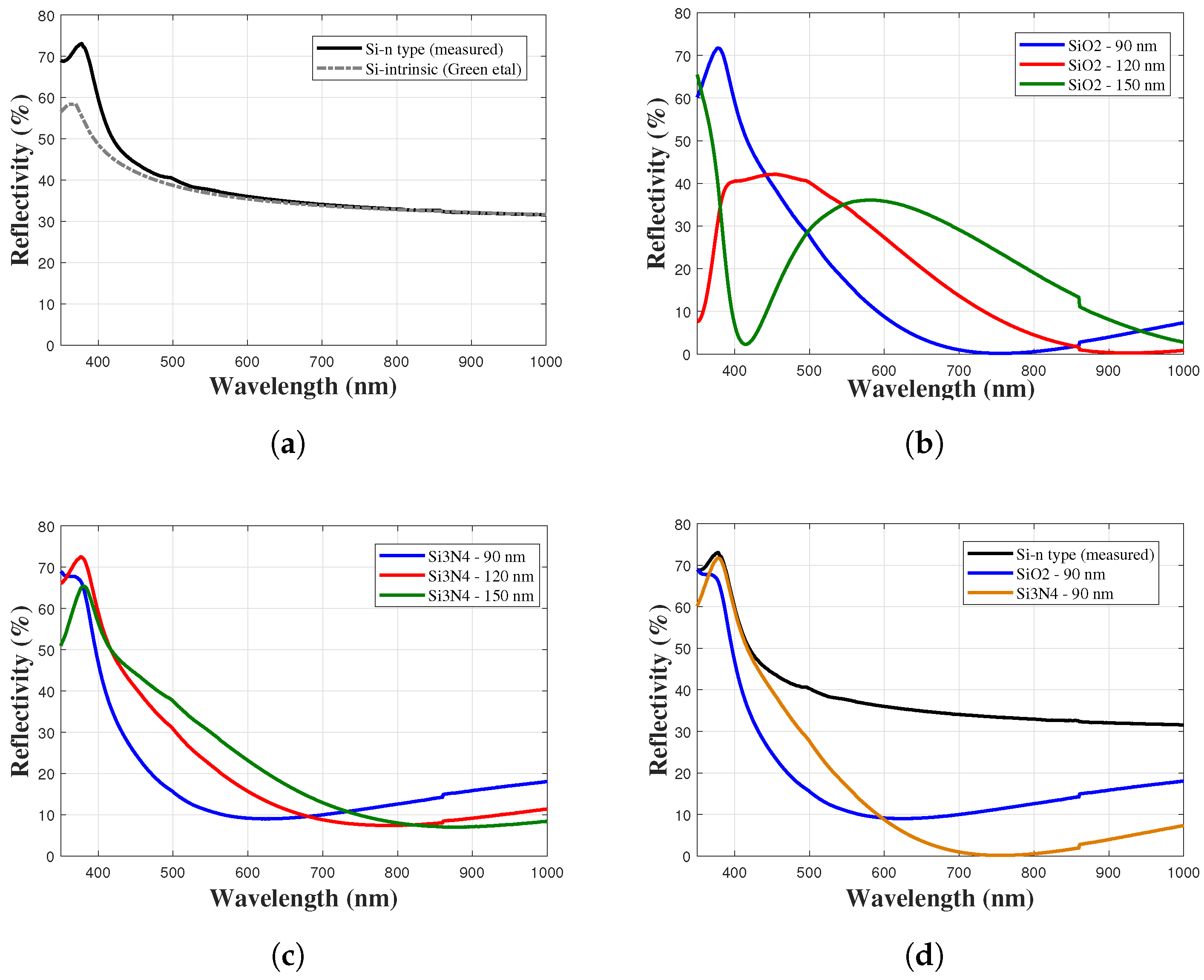
4.2. Optical Reflectivity Characteristics

Theoretically, the Fresnel equations describe the reflection and transmission of light when it encounters an interface between two different media. For normal incidence, the reflectivity R at an interface between two materials with refractive indices n 1 and n 2 is given by:
R = n 1 n 2 n 1 + n 2 2
When a thin film of refractive index n 2 and thickness d is applied to a substrate with refractive index n3, and the incident medium is air ( n 1 ≈ 1), the total reflectivity R t o t a l is influenced by interference effects. The reflectivity can be calculated using the following formula, which considers the constructive and destructive interference of light reflected from the top and bottom surfaces of the thin film:
R t o t a l = r 12 + r 23 e 2 i δ 1 + r 12 r 23 e 2 i δ 2
where r 12 is the reflection coefficient at the air–film interface, r 23 is the reflection coefficient at the film–substrate interface, and δ is the phase difference due to the path length in the film. These parameters can be calculated as follows:
r 12 = n 1 n 2 n 1 + n 2 r 23 = n 2 n 3 n 2 + n 3 δ = 2 π n 2 d λ
The optical reflectivity of n-type silicon substrates was systematically investigated, both in bare form and with the application of SiO2 or Si3N4 SLARCs. A series of samples were prepared, incorporating SLARC thicknesses of 90 nm, 100 nm, and 150 nm. Figure 3 presents the spectral reflectivity of these structures across a wavelength range of 350 nm to 1000 nm, with comparative data for intrinsic silicon included as a reference point [15,16].
Figure 3 presents a comparative analysis of reflectivity spectra for various n-type silicon substrates both with and without the application of SLARCs within the wavelength range of 350 nm to 1000 nm. The baseline reflectivity of n-type Si is established in Figure 3a, revealing comparable reflection characteristics to the reference intrinsic silicon spectrum. The introduction of SiO2 and Si3N4 SLARCs significantly reduces reflectivity, particularly within the visible spectrum, as evident in Figure 3b,c, with varying thicknesses. A correlation between SLARC thickness and reflectivity is observed, although interference effects can occur at greater thicknesses. However, The correlation between thickness and reflectivity exhibits variability across different wavelengths. While the refractive index remains relatively constant within the measured wavelength range, the relationship between SLARC thickness and reflectivity is not straightforward. Other factors, such as interference effects and material properties, likely influence the observed behavior. Figure 3d contrasts the reflectivity of SiO2 and Si3N4 SLARCs (both 90 nm-thick) with that of n-type Si, and highlights the superior anti-reflective properties of Si3N4 compared to SiO2 across a broader wavelength range. Notably, the Si3N4 SLARC with a thickness of 90 nm exhibits a minimum reflectivity of 0.16% at 750 nm compared to 9% for SiO2 counterpart at 650 nm.
The optimal spectral region for Si-SC light absorption spans from 350 nm to 1000 nm, with peak absorption efficiency typically occurring between 450 nm and 750 nm, centered around 600 nm. Table 1 provides a quantitative comparison of reflectivity values for n-type Si with and without SLARCs at key wavelengths within this range, alongside reference data for intrinsic Si. Both intrinsic and n-type Si exhibit relatively high reflectivity across the measured spectrum, with a decreasing trend towards longer wavelengths. The introduction of SiO2 and Si3N4 SLARCs significantly reduces reflectivity, particularly in the visible range (450 nm to 750 nm). SLARC thickness affects reflectivity, with thinner SiO2 SLARCs generally showing lower reflectivity. However, this trend is less pronounced for Si3N4 SLARCs. Reflectivity varies significantly with wavelength and SLARC thickness, highlighting the importance of considering the entire solar spectrum for SLARC and MLARC optimization. These experimental results serve as a foundation for subsequent modeling and simulation studies of Si-SC structures incorporating SLARCs and MLARCs.

5. Modeling and Simulating Si-SC Structures

To optimize Si-SC performance, a comprehensive modeling and simulation framework was employed. As illustrated in Figure 4, the optimization workflow of a two-step modeling approach was adopted. Initially, the optical properties of constituent materials (SiO2, Si3N4, LiF, and CdSe/ZnS NQDs) were experimentally determined, providing a foundation for subsequent simulations. These optical parameters, including refractive index and extinction coefficient, were incorporated into the Ansys−Lumerical−FDTD simulation environment.
Utilizing the FDTD method, the optical performance of various SLARC and MLARC configurations was meticulously analyzed. By systematically varying layer thicknesses, materials, and structural parameters, a comprehensive design space was explored. Key optical metrics, such as absorption, reflection, and transmission spectra, were assessed to identify optimal ARC designs that maximized light harvesting within the Si-SC.
To evaluate the electrical implications of the optimized ARC designs, the Lumerical CHARGE platform was integrated. Coupling optical generation data from FDTD simulations with device-level electrical models enabled a comprehensive assessment of Si-SC performance. Key electrical parameters, including short-circuit current, open-circuit voltage, and fill factor, were determined. Iterative optimization of ARC structures was conducted to achieve a balance between optical and electrical performance, ultimately enhancing overall Si-SC power conversion efficiency.

5.1. Optical Modeling and Simulation

A detailed understanding of light interaction with the Si-SC is essential for optimizing ARC design. The FDTD method was employed to compute the optical absorption spectrum across the relevant wavelength range (350 nm to 1100 nm). By considering the electric field intensity | E | and material permittivity i m g ( ε ) , the absorbed power ( Pabs ) was calculated using Equation (5).
Pabs = 0.5 ω × | E | 2 × i m g ( ε )
Quantum efficiency (QE), defined as the ratio of P a b s to incident power ( P i n ), was determined for each wavelength using Equation (6).
QE ( λ ) = P a b s ( λ ) P i n ( λ )
To provide spatial resolution of efficiency, local quantum efficiency (QElocal) was calculated, considering optical transmission and absorption at specific locations within the device:
QE l o c a l ( x , y , z ) = QE ( λ ) × T o p t ( x , y , z , λ ) × A o p t ( x , y , z , λ )
The optical generation rate per unit volume, denoted as G v ( λ ) , representing the rate at which electron–hole pairs are generated within a material per unit volume in response to incident photons at a specific wavelength λ , was calculated using:
G v ( λ ) = A o p t ( λ ) × I p h ( λ )
where I p h represents the incident photon flux at wavelength λ .

5.2. Electrical Modeling and Simulation

The electrical performance of the optimized ARC designs was assessed using the Lumerical CHARGE platform. By coupling optical generation data with device-level models, the short-circuit current density (Jsc) was calculated using Equation (9), considering the spatial distribution of carrier generation and local quantum efficiency.
J s c = ω q × G v ( x , y , z ) × QE l o c a l ( x , y , z ) d x d y d z
where q is elementary charge.
The open-circuit voltage (Voc) was estimated using Equation (10), incorporating Boltzmann statistics and the reverse saturation current density.
V o c = k T q ln ( J s c J o + 1 )
where k is the Boltzmann constant, T is the absolute temperature in Kelvin and Jo is the reverse saturation current density.
Finally, the power conversion efficiency (PCE) was determined using Equation (11), considering the fill factor (FF) calculated from the maximum power point.
PCE = J s c V o c F F P i n 1.5 G × 100 .
To comprehensively assess solar cell performance, both internal quantum efficiency (IQE) and external quantum efficiency (EQE) are essential metrics. EQE is determined by the interplay between optical efficiency (OE) and IQE. OE represents the fraction of incident light that is absorbed by the device, while IQE characterizes the efficiency of converting absorbed photons into collected charge carriers. Mathematically, EQE can be expressed as:
E Q E ( λ ) = O E ( λ ) × I Q E ( λ )
where OE is calculated as:
O E = 1 R T
with R and T representing the total reflected and transmitted power, respectively.
To accurately capture the optical and electrical behavior of Si-SCs, the FDTD simulations employed a refined mesh with a plane wave incident source covering the wavelength range of 350 nm to 1100 nm. Solar generation calculations were incorporated within the silicon layer to determine the spatial distribution of carrier generation. This comprehensive modeling approach provides a robust foundation for understanding the interplay between ARC design, optical properties, and electrical performance in Si-SCs.

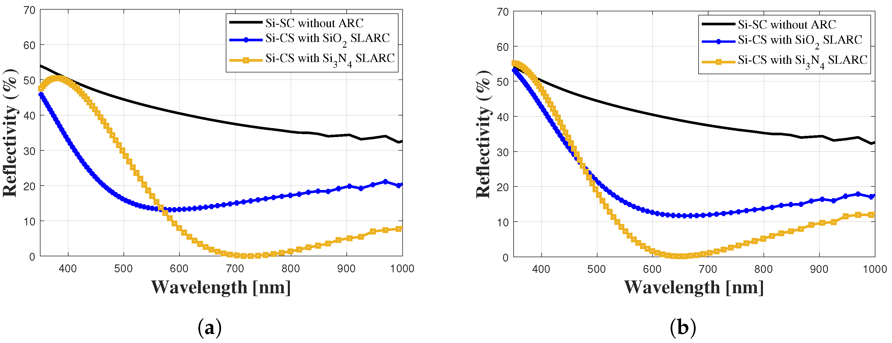
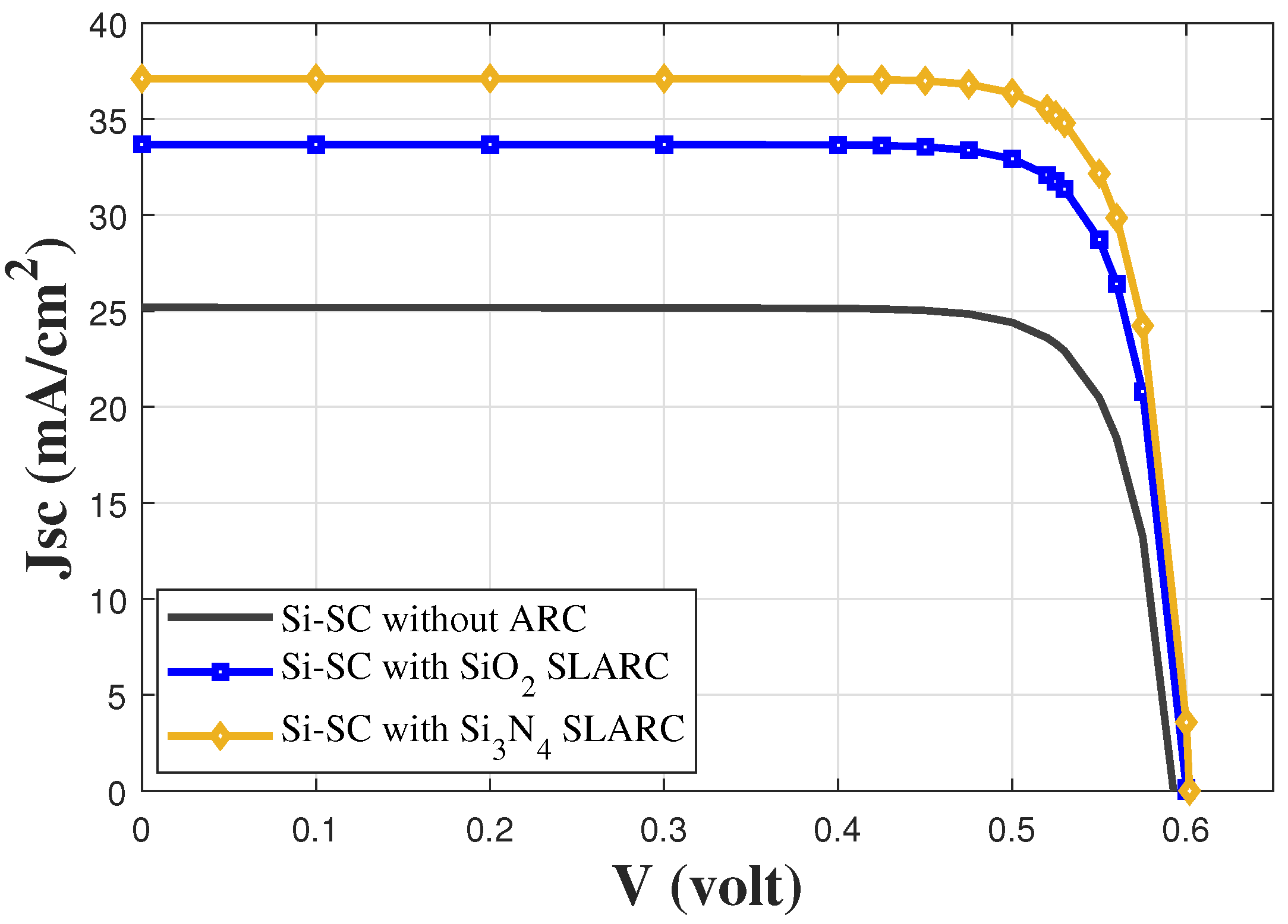
5.3. Modeling and Simulation of Si-SC with SLARC

The optical reflectivity of Si-SC structures with and without SLARCs was experimentally and numerically investigated. SLARCs composed of SiO2 and Si3N4, each with a thickness of 90 nm, were fabricated and characterized. Figure 5 presents the measured and simulated reflectivity spectra for these structures. A comparative analysis of reflectivity values at specific wavelengths is provided in Table 2. A strong correlation was observed between the experimental and simulated reflectivity data for Si-SC structures with and without SLARCs, validating the accuracy of the modeling approach.
The obtained reflectivity data, in conjunction with refractive index measurements, enabled the calculation of optimal SLARC thicknesses based on the quarter-wave principle at a reference wavelength of 550 nm. The resulting SLARC configurations (SiO2: 101 nm, Si3N4: 73 nm) were then simulated to assess their impact on reflectivity across the solar spectrum (Figure 5b).
To evaluate the electrical performance of the optimized SLARC structures, the IQE and EQE of Si-SCs were determined. The device structure was modeled using a top SiO2 or Si3N4 layer, a silver back reflector, and an aluminum emitter. Surface recombination velocities were assigned as follows: 1000 cm/s for aluminum, 107 cm/s for silver, and 1000 cm/s for both electrons and holes at the SiO2-Si and Si3N4-Si interfaces. In the electrical simulation, the electron and hole concentrations in the Si-SC are both set to 1 × 1020 cm−3 [20]. Table 3 presents a comparative analysis of IQE and EQE at selected wavelengths for Si-SCs with and without SLARC of SiO2 (101 nm) and Si3N4 (73 nm). While IQE provides insights into intrinsic material properties, EQE reflects the overall device efficiency, including optical losses. The observed discrepancies between IQE and EQE at shorter wavelengths highlight the impact of surface recombination on charge carrier collection.
The electrical characteristics of Si-SCs, including V o c , J s c , FF, and PCE, were determined using Lumerical CHARGE simulator. The calculated J-V curves (Figure 6) reveal the impact of SLARCs on device performance. The observed enhancement in J s c for SLARC-coated devices is attributed to the improved light harvesting efficiency, as evidenced by the reduced reflectivity.
Table 4 summarizes the key electrical performance parameters for Si-SC structures with and without SLARCs. The inclusion of SiO2 and Si3N4 SLARCs resulted in significant enhancements in J s c from 25.18 mA/cm2 to 37.11 mA/cm2, correspondingly increasing PCE from 12.27% to 18.47%. While V o c and FF remained relatively constant, the observed improvements in J s c and PCE directly correlate with the enhanced light harvesting capabilities of Si-SC with SLARCs, as evidenced by the IQE and EQE data.

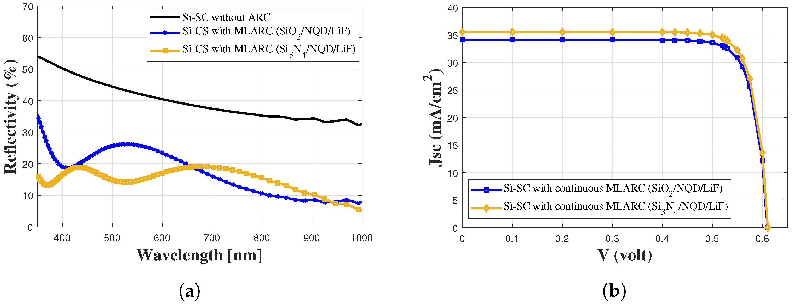
5.4. Modeling and Simulation of Si-SC with Continuous MLARC

The optical performance of continuous MLARC configurations comprising SiO2/NQD/ LiF and Si3N4/NQD/LiF was investigated using Lumerical FDTD simulations. The boundary conditions of the solver are set as periodic in the x and y directions to enable light propagation along the z-axis. Optimal layer thicknesses were determined through parametric studies, resulting in configurations of 40 nm SiO2, 40 nm NQD, and 100 nm LiF for the first structure, and 110 nm Si3N4, 50 nm NQD, and 70 nm LiF for the second.
Figure 7a compares the reflectivity of these MLARCs with the reference Si-SC structure. The SiO2/NQD/LiF MLARC demonstrated a significant reduction in reflectivity, particularly in the longer-wavelength region. While the Si3N4/NQD/LiF MLARC exhibited lower reflectivity across the entire spectrum, it showed a more pronounced reduction in the visible range. The implementation of continuous MLARC configurations yielded a substantial reduction in overall optical reflectivity compared to SLARC structures, underscoring the enhanced light-trapping capabilities of the multi-layer design.
To assess the impact of these MLARC configurations on Si-SC performance, IQE and EQE were calculated. Table 5 presents a comparative analysis of these parameters. Both MLARC configurations exhibited improved EQE compared to the SLARC structures, particularly at shorter wavelengths, attributed to the enhanced light harvesting capabilities of the NQD layer, facilitated by its downshifting effect. However, the Si3N4/NQD/LiF configuration showed a decrease in EQE at longer wavelengths, due to the change in the reflectivity.
The electrical performance of Si-SCs with continuous MLARCs was evaluated through J-V characteristic simulations, as shown in Figure 7b. In addition, Table 6 summarizes the key electrical performance parameters for Si-SC structures with and without MLARCs. The calculated J s c values for the SiO2/NQD/LiF and Si3N4/NQD/LiF configurations were 34.1 mA/cm2 and 35.54 mA/cm2, respectively, representing improvements over the SLARC-based Si-SCs. Corresponding PCE values of 17.26% and 18.02% were obtained.

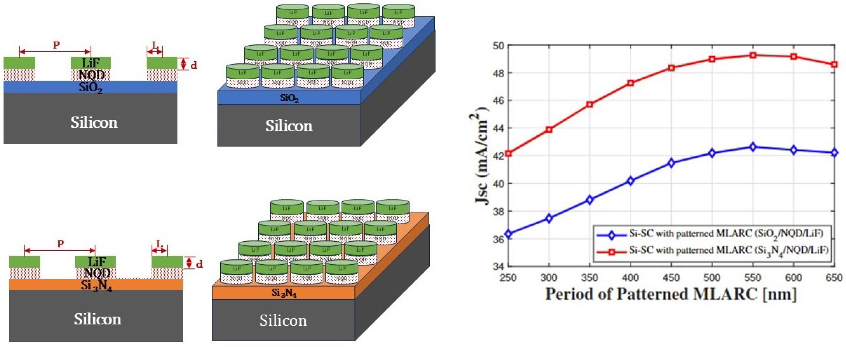
5.5. Modeling and Simulation of Si-SC with Patterned MLARC

To investigate the potential of patterned MLARCs, the SiO2/NQD/LiF and Si3N4/NQD/LiF configurations were simulated using Lumerical FDTD. As shown in Figure 8, the geometric parameters, including layer thicknesses (d), period (P), and radius (L) of the cylindrical patterns, were optimized. The Lumerical FDTD simulation tool was employed to simulate these structures, with periodic boundary conditions applied in the x and y directions to mimic an infinite array of patterns, while light propagation was modeled along the z-axis.
The optimization of patterned MLARCs involved a systematic variation of the period (P) of the cylindrical patterns, while maintaining a constant L/P ratio of approximately 0.32 . This approach allowed for an assessment of the impact of pattern periodicity on the overall device performance. By simulating Si-SC structures with varying P values within the range of 250   n m to 600   n m , the sensitivity of J s c to the pattern period was investigated. As depicted in Figure 8, J s c initially increases with increasing P, reaching a maximum value at an optimal period before decreasing at larger P values. This behavior indicates the existence of an optimal pattern periodicity that maximizes light trapping and carrier generation.
The observed trend can be attributed to the interplay between light scattering, diffraction, and interference effects within the patterned structure. At smaller periods, light scattering is less efficient, leading to reduced light trapping. Conversely, at larger periods, excessive light scattering can occur, resulting in increased reflection losses. The optimal period represents a balance between these competing effects, maximizing light absorption and minimizing reflection. By conducting a parametric study across a range of d, P, and L values, through rigorous optimization, the following d values were determined: 80 nm SiO2, 40 nm NQD, and 60 nm LiF for the SiO2/NQD/LiF configuration; 60 nm Si3N4, 60 nm NQD, and 60 nm LiF for the Si3N4/NQD/LiF configuration. The cylindrical patterns of NQD and LiF layers were optimized with (P) of 550 nm and (L) of 175 nm. The optimization analysis identified the optimal geometric parameters of the pattern for each MLARC configuration, providing valuable insights for the design of high-performance Si-SCs.
Figure 9a presents the reflectivity spectra of the patterned MLARC configurations. Both structures exhibited significantly reduced reflectivity compared to their continuous counterparts, particularly in the visible and near-infrared regions. The Si3N4/NQD/LiF configuration demonstrated superior light trapping capabilities, achieving a minimum reflectivity of 5% at 550 nm.
The impact of patterned MLARCs on carrier generation was assessed through IQE and EQE calculations. Table 7 presents the results, indicating a substantial enhancement in EQE for both configurations compared to the SLARC and continuous MLARC counterparts. This improvement is attributed to the combined effects of light trapping of the optimized cylindrical patterns and downshifting within the NQD layer.
To evaluate the electrical performance of patterned MLARCs, J-V characteristics were simulated, as shown in Figure 9b. In addition, Table 8 summarizes the key electrical performance parameters for Si-SC structures with and without patterned MLARCs. The calculated J s c values for the SiO2/NQD/LiF and Si3N4/NQD/LiF patterned MLARCs were 39.51 mA/cm2 and 48.04 mA/cm2, respectively, representing significant improvements over the continuous MLARC and SLARC configurations. The corresponding PCE values were 20.12% and 24.65%.
Overall, the optimized patterned MLARC structures exhibited reduced reflectivity compared to their continuous counterparts, with the Si3N4/NQD/LiF configuration demonstrating superior performance. The introduction of periodic patterns led to enhanced light trapping and improved absorption, as evidenced by the increased IQE and EQE values. These findings were further corroborated by the electrical performance analysis, which revealed significant improvements in J s c and PCE for the patterned MLARC structures.
By correlating microscopic optical properties with macroscopic device performance, Table 9 presents a comparative overview of reflectivity, EQE, J s c , and PCE for different Si-SC structures. The results underscore the significant impact of ARC design on light absorption and charge carrier generation to optimize light management and enhance Si-SC performance. The enhanced performance of Si-SC with patterned MLARCs can be attributed to several factors:
  • Improved light trapping: The periodic patterns scatter incident light, increasing the optical path length within the active region and promoting multiple reflections, leading to enhanced light absorption.
  • Enhanced carrier generation: The NQD layer absorbs photons at shorter wavelengths and re-emits them at longer wavelengths through a downshifting process. These downshifted photons are more effectively absorbed by the semiconductor layer, resulting in increased carrier generation.
  • Reduced reflection losses: The optimized pattern design minimizes reflection at the top surface of the solar cell, allowing a higher proportion of incident light to be coupled into the device.
These combined effects contribute to the significant improvements in Jsc, EQE, and overall PCE observed for the patterned MLARC configurations.

6. Conclusions

This study underscores the pivotal role of ARCs in enhancing Si-SC efficiency. By systematically investigating SLARCs, continuous MLARCs, and patterned MLARCs, we have demonstrated the effectiveness of these approaches in mitigating reflection losses and optimizing light absorption. The incorporation of NQDs within micro-/nano-patterned MLARCs further amplified light trapping and absorption, leading to substantial improvements in device performance. By combining experimental characterization and numerical modeling, this research demonstrated that the optimized patterned MLARC configuration achieved a 45% reduction in reflectivity relative to the reference Si-SC, ultimately contributing to overall performance gains.
The results presented herein highlight the potential of advanced ARC technologies to significantly enhance Si-SC efficiency. While this study has focused on optical and electrical performance, future research should explore the integration of these optimized ARC designs with strategies to address electrical and thermal losses. By combining these advancements, the realization of high-efficiency, cost-effective silicon-based solar cells can be accelerated.

Author Contributions

Conceptualization, I.H.K., A.H.S., T.I. and B.E.A.-E.; methodology, I.H.K., A.H.S., T.I. and B.E.A.-E.; software, T.I. and B.E.A.-E.; validation, A.H.S., I.H.K. and T.I.; formal analysis, B.E.A.-E.; investigation, T.I.; resources, A.H.S.; data curation, I.H.K.; writing—original draft preparation, B.E.A.-E.; writing—review and editing, I.H.K., T.I. and A.H.S.; visualization, I.H.K.; supervision, T.I.; project administration, A.H.S.; funding acquisition, I.H.K. All authors have read and agreed to the published version of the manuscript.

Funding

This research was funded by RC-442/44.

Institutional Review Board Statement

Not applicable.

Informed Consent Statement

Not applicable.

Data Availability Statement

The original contributions presented in the study are included in the article; further inquiries can be directed to the first author.

Acknowledgments

The authors extend their appreciation to Taibah University, represented by the Deanship of Scientific Research, for funding this project No. (RC-442/44).

Conflicts of Interest

The authors declare no conflicts of interest.

References

  1. Machín, A.; Márquez, F. Advancements in Photovoltaic Cell Materials: Silicon, Organic, and Perovskite Solar Cells. Materials 2024, 17, 1165. [Google Scholar] [CrossRef] [PubMed]
  2. Hossain, M.J.; Sun, M.; Davis, K.O. Photon management in silicon photovoltaic cells: A critical review. Sol. Energy Mater. Sol. Cells 2024, 267, 112715. [Google Scholar] [CrossRef]
  3. Dhawan, P.; Gaudig, M.; Sprafke, A.; Piechulla, P.; Wehrspohn, R.B.; Rockstuhl, C. Anti-Reflective Graded-Index Metasurface with Correlated Disorder for Light Management in Planar Silicon Solar Cells. Adv. Opt. Mater. 2024, 12, 2302964. [Google Scholar] [CrossRef]
  4. Valiei, M.; Shaibani, P.M.; Abdizadeh, H.; Kolahdouz, M.; Asl Soleimani, E.; Poursafar, J. Design and optimization of single, double and multilayer anti-reflection coatings on planar and textured surface of silicon solar cells. Mater. Today Commun. 2022, 32, 104144. [Google Scholar] [CrossRef]
  5. Ovcharenko, O.; Dyakonenko, N.; Tavrina, T.; Lyubchenko, O. Computation of the parameters of single- and double-layer anti-reflective coatings for their effective use. In Proceedings of the 2022 IEEE 3rd KhPI Week on Advanced Technology (KhPIWeek), Kharkiv, Ukraine, 3–7 October 2022; pp. 1–5. [Google Scholar] [CrossRef]
  6. Addie, A.J.; Ismail, R.A.; Mohammed, M.A. Amorphous carbon nitride dual-function anti-reflection coating for crystalline silicon solar cells. Sci. Rep. 2022, 12, 9902. [Google Scholar] [CrossRef] [PubMed]
  7. Dumont, L.; Benzo, P.; Cardin, J.; Yu, I.S.; Labbe, C.; Marie, P.; Dufour, C.; Zatryb, G.; Podhorodecki, A.; Gourbilleau, F. Down-shifting Si-based layer for Si solar applications. Sol. Energy Mater. Sol. Cells 2017, 169, 132–144. [Google Scholar] [CrossRef]
  8. Lv, T.; Tang, Y.; Fan, H.; Liu, S.; Zeng, S.; Liu, W. Carbon quantum dots anchored on the anti-reflection silica layer as solid luminescence down-shifting materials in solar panel encapsulation. Sol. Energy Mater. Sol. Cells 2022, 235, 111450. [Google Scholar] [CrossRef]
  9. Feng, B.; Chen, W.; Xing, G.; Chen, X.; Li, H.; Sun, Z.; Zhang, Y.; Liu, Y.; Du, X. Influence of inverted pyramid texturization on front metallization and performance of crystalline silicon solar cells. Sol. Energy Mater. Sol. Cells 2024, 272, 112919. [Google Scholar] [CrossRef]
  10. Lopez-Delgado, R.; Higuera-Valenzuela, H.; Zazueta-Raynaud, A.; Ramos-Carrazco, A.; Pelayo, J.; Berman-Mendoza, D.; Álvarez-Ramos, M.; Ayon, A. Solar cell efficiency improvement employing down-shifting silicon quantum dots. Microsyst. Technol. 2018, 24, 495–502. [Google Scholar] [CrossRef]
  11. Flores-Pacheco, A.; Álvarez-Ramos, M.E.; Ayón, A. Down-shifting by quantum dots for silicon solar cell applications. In Solar Cells and Light Management; Elsevier: Amsterdam, The Netherlands, 2020; pp. 443–477. [Google Scholar]
  12. Masaadeh, Q.; Kaplani, E.; Chao, Y. Luminescent downshifting silicon quantum dots for performance enhancement of polycrystalline silicon solar cells. Electronics 2022, 11, 2433. [Google Scholar] [CrossRef]
  13. Sabeeh, A.H.; Price, J.S.; Ruzyllo, J. Effect of lift-off conditions on micropatterning of nanocrystalline quantum dot films. J. Vac. Sci. Technol. B 2017, 35, 061802. [Google Scholar] [CrossRef]
  14. Sabeeh, A.H.; Brigeman, A.N.; Ruzyllo, J. Performance of single-crystal silicon solar cells with mist-deposited nanocrystalline quantum dot downshifting films. IEEE J. Photovolt. 2019, 9, 1006–1011. [Google Scholar] [CrossRef]
  15. Green, M.A.; Keevers, M.J. Optical properties of intrinsic silicon at 300 K. Prog. Photovolt. Res. Appl. 1995, 3, 189–192. [Google Scholar] [CrossRef]
  16. Green, M.A. Improved silicon optical parameters at 25 C, 295 K and 300 K including temperature coefficients. Prog. Photovolt. Res. Appl. 2022, 30, 164–179. [Google Scholar] [CrossRef]
  17. Arkhipov, V.; Poortmans, J. Thin Film Polycrystalline Silicon Solar Cells. In Thin Film Solar Cells: Fabrication, Characterization and Applications; Wiley: Hoboken, NJ, USA, 2006; pp. 97–131. [Google Scholar]
  18. Dement, D.B.; Puri, M.; Ferry, V.E. Determining the Complex Refractive Index of Neat CdSeCdS Quantum Dot Films. J. Phys. Chem. C 2018, 122, 21557–21568. [Google Scholar] [CrossRef]
  19. Dauer, V. Optical constants of lithium fluoride thin films in the far ultraviolet. J. Opt. Soc. Am. B 2000, 17, 300–303. [Google Scholar] [CrossRef]
  20. Hussain, S.; Mehmood, H.; Khizar, M.; Turan, R. Design and analysis of an ultra-thin crystalline silicon heterostructure solar cell featuring SiGe absorber layer. IET Circuits Devices Syst. 2018, 12, 309–314. [Google Scholar] [CrossRef]
Figure 1. Schematic representation of silicon solar cell (Si-SC) structures. (a) Si-SC with single-layer anti-reflection coating (SLARC). (b) Si-SC with multi-layer anti-reflection coating (MLARC), including continuous and micro-/nano-patterned configurations. The SLARC and MLARC consist of SiO2, Si3N4, NQDs, and LiF layers.
Applsci 15 03053 g001
Figure 2. Refractive index spectra of single-layer thin films comprising SiO2, Si3N4, CdSe/ZnS NQDs, and LiF deposited on n-type Si wafers. Measurements were conducted at room temperature over a wavelength range of 350 to 1000 nm. Reference data for intrinsic silicon at 300 K are included (Green and Keevers [15,16]).
Applsci 15 03053 g002
Figure 3. Optical reflectivity of (a) bare n-type silicon and intrinsic silicon (reference data from Green and Keevers [15,16]), (b) n-type silicon with SiO2 SLARC, (c) n-type silicon with Si3N4 SLARC, and (d) comparative reflectivity of bare silicon, SiO2 SLARC (90 nm), and Si3N4 SLARC (90 nm). Measurements were performed at room temperature over a wavelength range of 350 to 1000 nm.
Applsci 15 03053 g003
Figure 4. Optimization process for designing and evaluating the optical and electrical characteristics of Si-SC with SLARC and MLARC.
Applsci 15 03053 g004
Figure 5. The reflectivity spectra of Si-SCs with and without SLARCs: (a) measured reflectivity of Si-SC with SiO2 SLARC (90 nm), and Si-SC with Si3N4 ARC (90 nm), and (b) simulated reflectivity of Si-SC with and without SiO2 and Si3N4 SLARCs (quarter-wave thickness). All measurements and simulations were performed at room temperature over a wavelength range of 350 nm to 1000 nm.
Applsci 15 03053 g005
Figure 6. Current–voltage (J-V) characteristics of Si-SC structures with and without SLARC of SiO2 (101 nm) and Si3N4 (73 nm).
Applsci 15 03053 g006
Figure 7. (a) Simulated reflectivity spectra and (b) current–voltage (J-V) characteristics for Si-SC structures with continuous MLARC of SiO2/NQD/LiF and Si3N4/NQD/LiF configurations.
Applsci 15 03053 g007
Figure 8. Sensitivity of J s c to the pattern period at different geometric parameters, including patterns periodic (P) and radius (L) with L/P ratio = 0.32 , for Si-SC structures with patterned MLARC configurations: SiO2/NQD/LiF and Si3N4/NQD/LiF.
Applsci 15 03053 g008
Figure 9. (a) Simulated reflectivity spectra and (b) current–voltage (J-V) characteristics for Si-SC structures with patterned MLARC of SiO2/NQD/LiF and Si3N4/NQD/LiF configurations.
Applsci 15 03053 g009
Table 1. Measured reflectivity of n-type Si substrates with and without SLARCs at different thicknesses and wavelengths, against reflectivity of intrinsic Si (reference data from Green and Keevers [15]).
StructureThickness (nm)Wavelength (nm)
350450550650750
Si (no ARC)intrinsic56.4541.9636.7334.7333.24
Si (no ARC)n-type68.9844.1837.6334.9333.43
Si with SiO2 SLARC9068.9524.6710.859.1511.24
12066.1540.7022.1011.347.64
15050.9744.2330.0217.379.88
Si with Si3N4 SLARC9060.2039.7616.773.640.16
1207.6242.1134.3520.158.36
15065.4612.9235.3033.3124.17
Table 2. Measured and simulated reflectivity of Si-SC structures with and without SLARC of SiO2 (90 nm) and Si3N4 (90 nm).
StructureTypeWavelength (nm)
350450550650750
Si-SC (no ARC)measured68.9844.1837.6334.9333.43
simulated51.9845.7741.5038.4535.86
Si-SC with SiO2 SLARCmeasured68.9524.6710.859.1511.24
simulated46.6222.5213.5213.8516.27
Si-SC with Si3N4 SLARCmeasured60.2039.7616.773.640.16
simulated47.5441.6116.982.580.23
Table 3. IQE and EQE of Si-SC structures with and without SLARCs of SiO2 (101 nm) and Si3N4 (73 nm), at selected wavelengths: 350, 550, and 750 nm.
IQE ( % ) EQE ( % )
Structure350550750350550750
Si-SC (no ARC)90.5496.7199.3643.4656.5763.49
Si-SC with SiO2 SLARC95.9396.6999.4746.6582.1987.13
Si-SC with Si3N4 SLARC90.5596.6099.2541.8193.1494.05
Table 4. Electrical characteristics of Si-SC structures with and without SLARCs of SiO2 (101 nm) and Si3N4 (73 nm).
Structure V oc ( V ) J sc (mA/cm2)FFPCE (%)
Si-SC (no ARC) 0.59 25.18 0.82 12.27
Si-SC with SiO2 SLARC 0.60 33.67 0.82 16.68
Si-SC with Si3N4 SLARC 0.60 37.11 0.82 18.47
Table 5. IQE and EQE of Si-SC structures with and without continuous MLARCs of SiO2/NQD/LiF and Si3N4/NQD/LiF configurations, at selected wavelengths: 350, 550, and 750 nm.
IQE ( % ) EQE ( % )
Structure350550750350550750
Si-SC (no ARC)90.5496.7199.3643.4656.5763.49
Si-SC with SiO2/NQD/LiF C-MLARC96.4998.1299.5963.0972.7386.96
Si-SC with Si3N4/NQD/LiF C-MLARC96.4898.3499.5181.1683.9382.07
Table 6. Electrical characteristics for Si-SC structures with and without continuous MLARC of SiO2/NQD/LiF and Si3N4/NQD/LiF configurations.
Structure V oc ( V ) J sc (mA/cm2)FFPCE (%)
Si-SC (no ARC) 0.59 25.18 0.82 12.27
Si-SC with SiO2/NQD/LiF C-MLARC 0.61 34.10 0.83 17.26
Si-SC with Si3N4/NQD/LiF C-MLARC 0.61 35.54 0.83 18.02
Table 7. IQE and EQE of Si-SC structures with patterned MLARCs of SiO2/NQD/LiF and Si3N4/NQD/LiF configurations.
IQE (%)EQE (%)
Structure350550750350550750
Si-SC (no ARC)90.5496.7199.3643.4656.5763.49
Si-SC with SiO2/NQD/LiF P-MLARC96.4798.1299.5058.3986.3587.27
Si-SC with Si3N4/NQD/LiF P-MLARC95.9597.8099.4164.6294.9695.08
Table 8. Electrical characteristics for Si-SC structures with patterned MLARC of SiO2/NQD/LiF and Si3N4/NQD/LiF configurations.
Structure V oc ( V ) J sc (mA/cm2)FFPCE (%)
Si-SC (no ARC) 0.59 25.18 0.82 12.27
Si-SC with SiO2/NQD/LiF P-MLARC 0.61 39.52 0.83 20.13
Si-SC with Si3N4/NQD/LiF P-MLARC 0.62 48.04 0.83 24.65
Table 9. Optical and electrical characteristics for Si-SC structures with no ARC, SLARC, continuous (C-MLARC) and patterned (P-MLARC) of SiO2/NQD/LiF and Si3N4/NQD/LiF configurations.
StructureOptical ParametersElectrical Parameters
350 (nm)550 (nm)750 (nm)-
R
(%)
EQE
(%)
R
(%)
EQE
(%)
R
(%)
EQE
(%)
J
(mA/cm2)
PCE
(%)
Si-SC
(no ARC)
51.9843.4641.5056.5735.8663.4925.1812.27
Si-SC
(SiO2 SLARC)
51.8546.6514.9982.1912.3987.1333.6716.68
Si-SC
(SiO2 C-MLARC)
34.6263.0925.6872.7312.6886.9634.1017.26
Si-SC
(SiO2 P-MLARC)
39.4758.3911.9986.3512.1687.2739.5220.13
Si-SC
(Si3N4 SLARC)
53.8341.813.5893.145.0194.0537.1118.47
Si-SC
(Si3N4 C-MLARC)
15.8981.1614.6583.9417.5282.0735.5418.02
Si-SC
(Si3N4 P-MLARC)
32.6464.622.9194.964.3595.0848.0424.65
Disclaimer/Publisher’s Note: The statements, opinions and data contained in all publications are solely those of the individual author(s) and contributor(s) and not of MDPI and/or the editor(s). MDPI and/or the editor(s) disclaim responsibility for any injury to people or property resulting from any ideas, methods, instructions or products referred to in the content.

