
Additive Manufacturing for Automotive Radar Sensors Using Copper Inks and Pastes


Abstract
Featured Application
Abstract
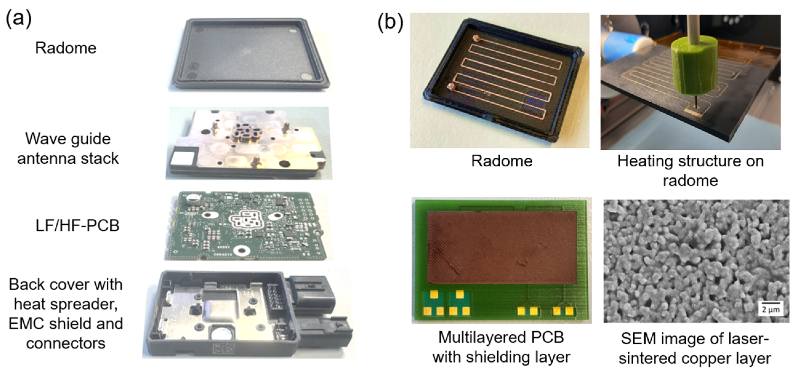
1. Introduction
2. Materials and Methods
2.1. Materials
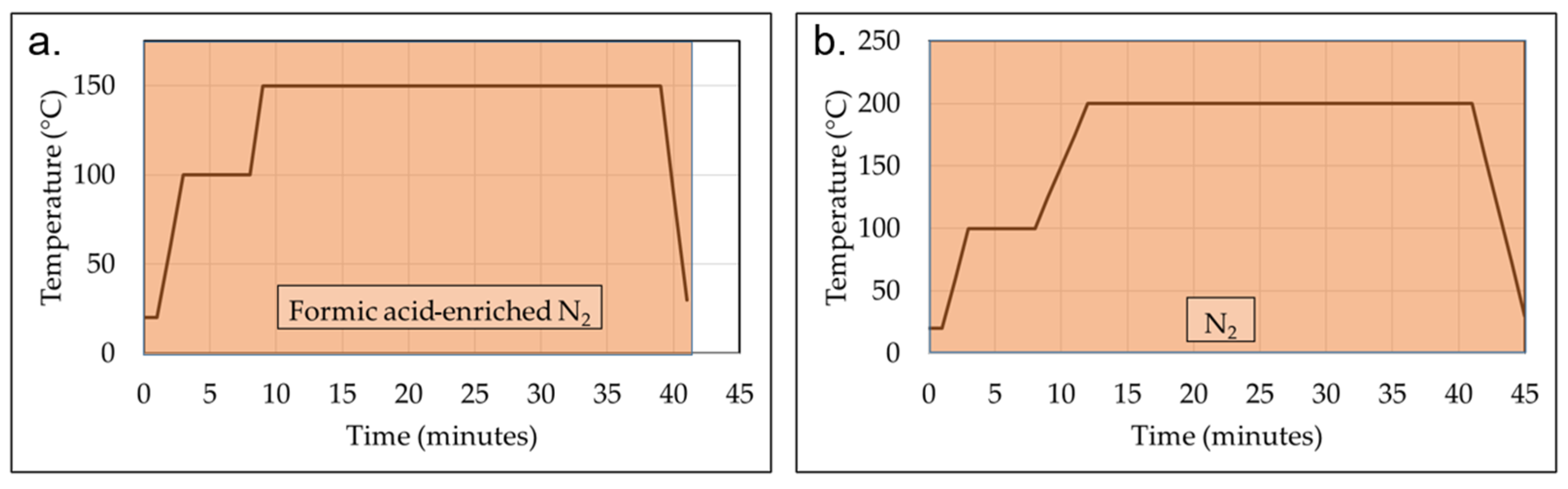
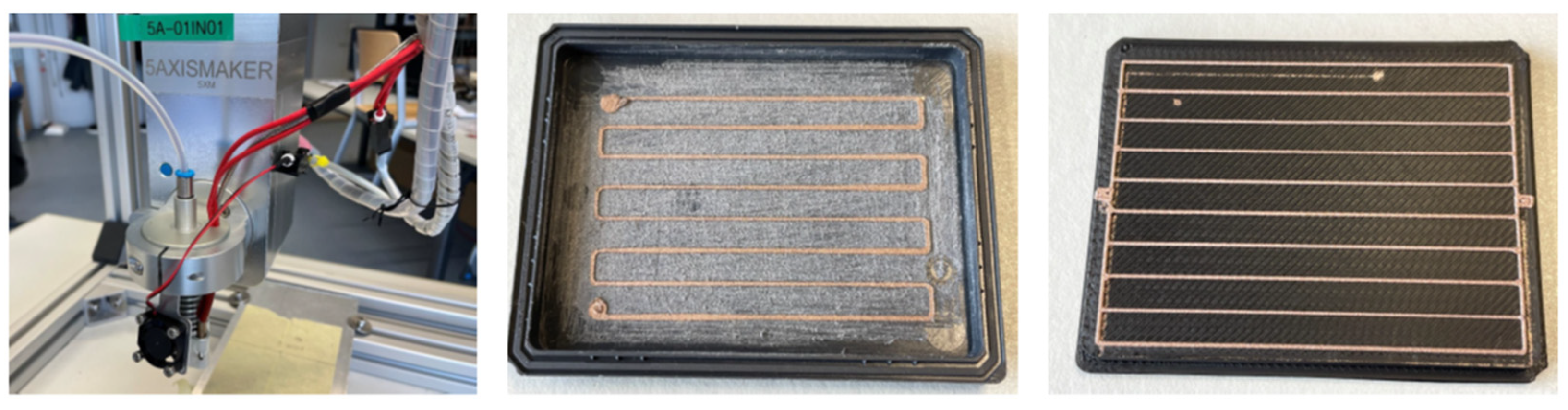
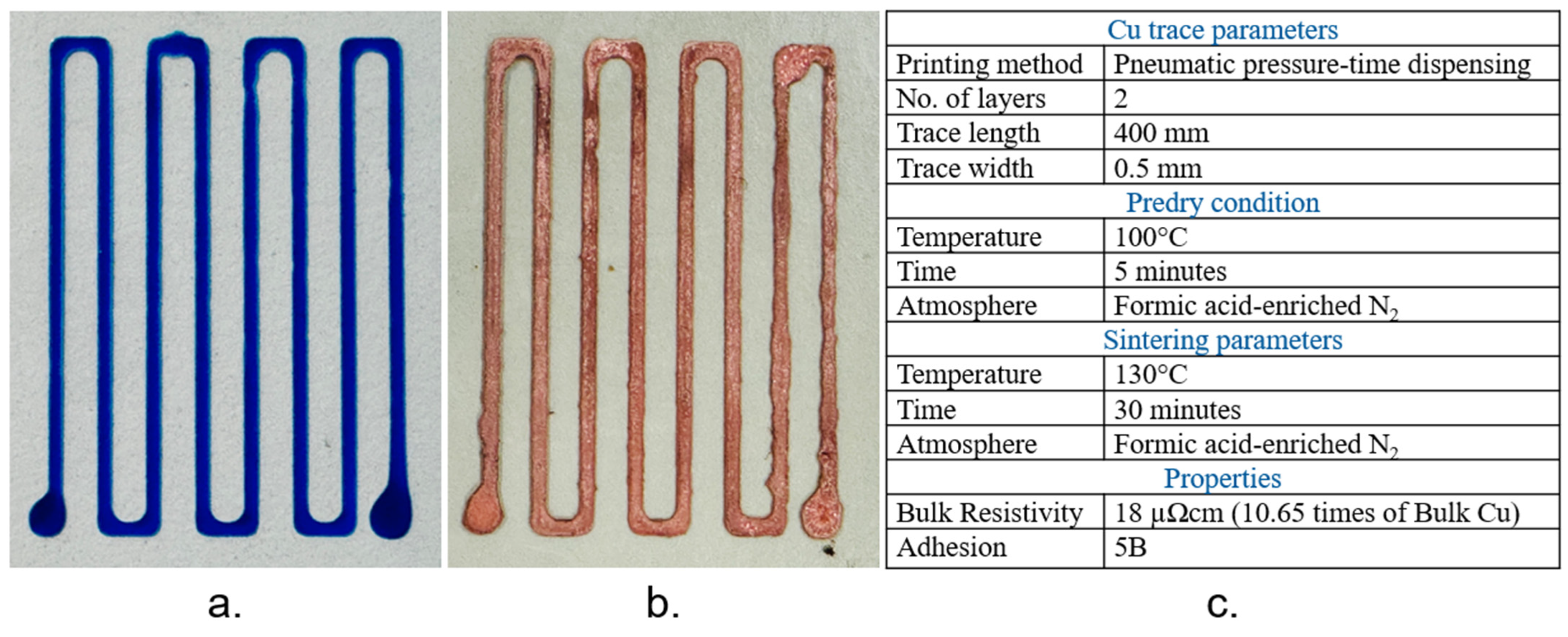
2.2. Preparation, Application, and Sintering
2.3. Characterization Methods
3. Results and Discussion
3.1. Simulation-Driven Heating Structure Design
3.2. Fused Deposition Modeling
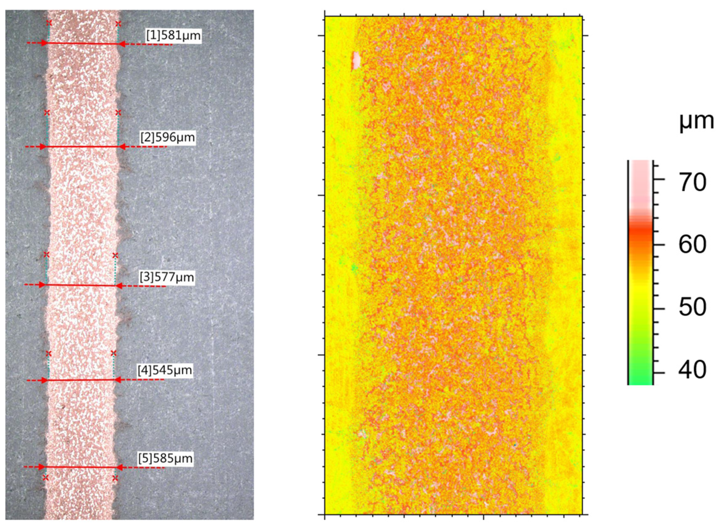
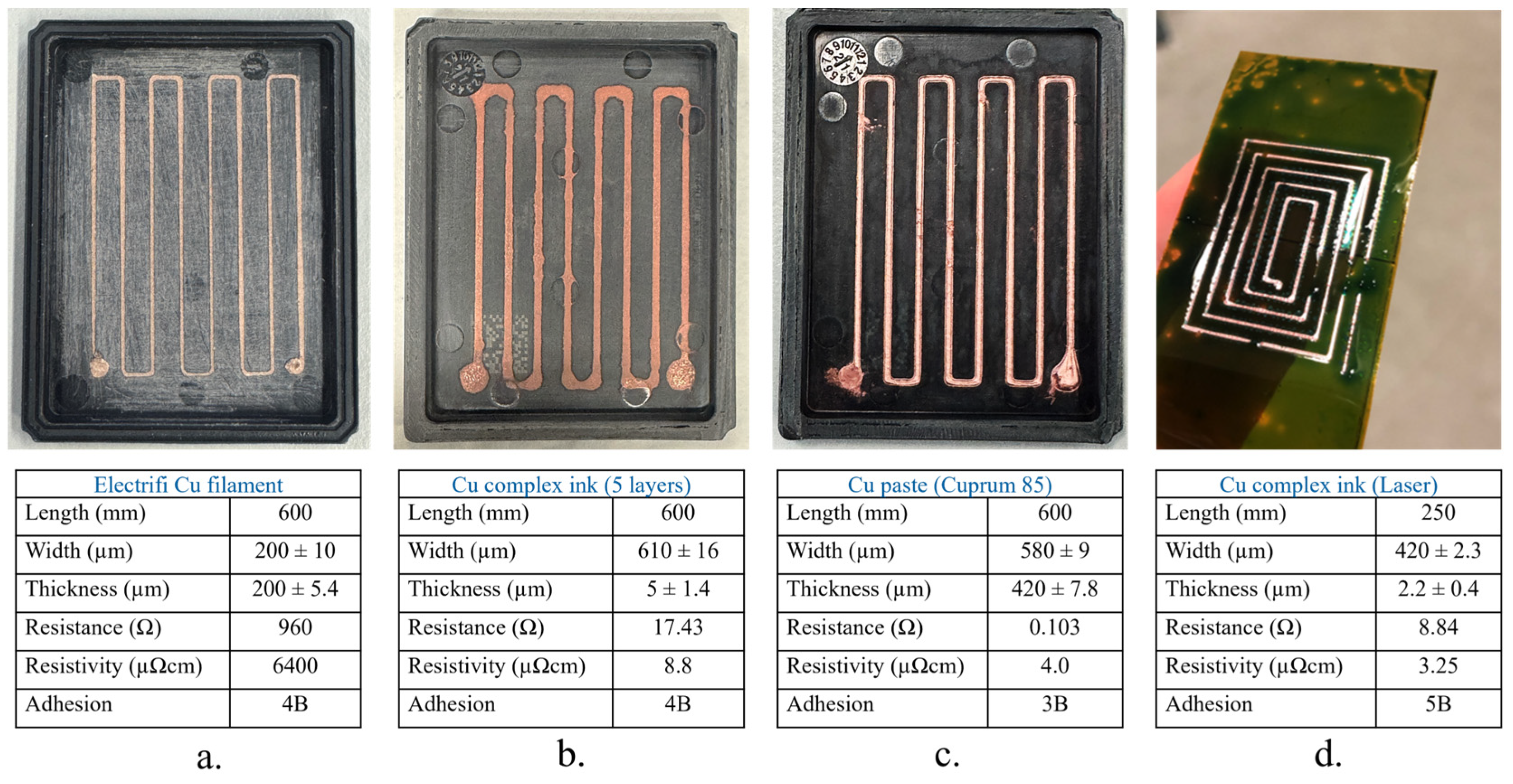
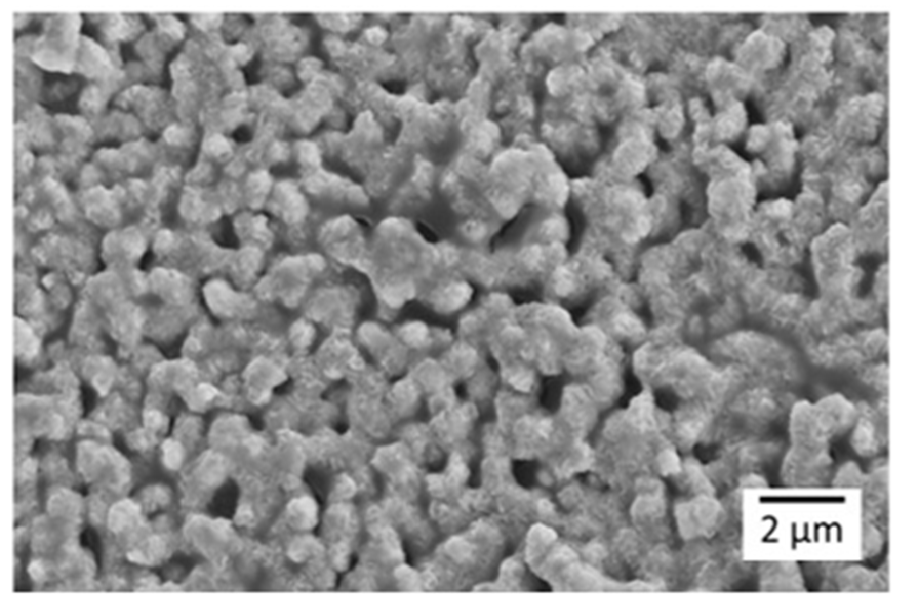
3.3. Heating Structure Formed by Copper Ink and Paste
4. Conclusions
Author Contributions
Funding
Institutional Review Board Statement
Informed Consent Statement
Data Availability Statement
Acknowledgments
Conflicts of Interest
References
- Mallaiah, M.; Thapliyal, S.; Bose, S.C. Recent Advances in Additive Manufacturing; Springer Nature: Singapore, 2022; Volume 1, ISBN 978-981-97-6016-9. [Google Scholar]
- Gao, W.; Zhang, Y.; Ramanujan, D.; Ramani, K.; Chen, Y.; Williams, C.B.; Wang, C.C.L.; Shin, Y.C.; Zhang, S.; Zavattieri, P.D. The Status, Challenges, and Future of Additive Manufacturing in Engineering. Comput. Aided Des. 2015, 69, 65–89. [Google Scholar] [CrossRef]
- Massetti, M.; Zhang, S.; Harikesh, P.C.; Burtscher, B.; Diacci, C.; Simon, D.T.; Liu, X.; Fahlman, M.; Tu, D.; Berggren, M.; et al. Fully 3D-printed organic electrochemical transistors. npj Flex Electron 2023, 7, 11. [Google Scholar] [CrossRef]
- Dong, Y.; Bao, C.; Kim, W.S. Sustainable additive manufacturing of printed circuit boards. Joule 2018, 2, 579–582. [Google Scholar] [CrossRef]
- Lüngen, S.; Tiedje, T.; Meier, K.; Nieweglowski, K.; Bock, K. Reliability of 3D Additive Manufactured Packages. In Proceedings of the 7th Electronic System-Integration Technology Conference (ESTC), Dresden, Germany, 18–21 September 2018; pp. 1–5. [Google Scholar] [CrossRef]
- Tan, H.W.; Tran, T.; Chua, C.K. A Review of Printed Passive Electronic Components through Fully Additive Manufacturing Methods. Virtual Phys. Prototyp. 2016, 11, 271–288. [Google Scholar] [CrossRef]
- Perry, T.S. In Search of the Future of Air Traffic Control. IEEE Spectr. 1997, 34, 18–35. [Google Scholar] [CrossRef]
- Schmullius, C.C.; Evans, D.L. Synthetic Aperture Radar (SAR) Frequency and Polarization Requirements for Applications in Ecology, Geology, Hydrology, and Oceanography: A Tabular Status Quo After SIR-C/X-SAR. Int. J. Remote Sens. 1997, 18, 2713–2722. [Google Scholar] [CrossRef]
- Steigemann, M.; Vaucher, C.S. Modern Radar Sensors in Advanced Automotive Architectures. In Radar for Fully Autonomous Driving; Markel, M., Ed.; Artech House: London, UK, 2022; pp. 3–24. ISBN 9781630818975. [Google Scholar]
- Mohammad, E. Radar Technology. In Advanced Driver Assistance Systems and Autonomous Vehicles from Fundamentals to Applications; Li, E., Shi, H., Eds.; Springer Nature: Singapore, 2022; pp. 265–304. [Google Scholar]
- ISO 16750-1:2023Road Vehicles—Environmental Conditions and Testing for Electrical and Electronic Equipment; International Organization for Standardization: Geneva, Switzerland, 2023.
- Huegel, U.; Garcia-Tejero, A.; Glogowski, R.; Willmann, E.; Pieper, M.; Merli, F. 3D Waveguide Metallized Plastic Antennas Aim to Revolutionize Automotive Radar. Microw. J. 2022, 65, 32. [Google Scholar]
- Jozwicka, M.; Garcia-Tejero, A.; Bekker, E.; Kowalewski, J.; Merli, F.; Zwick, T. 3D Printed Metallized Polymer Slotted Waveguide Antenna Array for Automotive Radar Applications at 140 GHz. In Proceedings of the IEEE/MTT-S International Microwave Symposium—IMS, San Diego, CA, USA, 11–16 June 2023. [Google Scholar] [CrossRef]
- Menzel, W. Antennas in Automobile Radar. In Handbook of Antenna Technologies; Chen, Z., Liu, D., Nakano, H., Qing, X., Zwick, T., Eds.; Springer: Singapore, 2016. [Google Scholar] [CrossRef]
- Di Fabrizio, G.; Calisti, L.; Contoli, C.; Kania, N.; Lattanzi, E. A Study on the Energy-Efficiency of the Object Tracking Algorithms in Edge Devices. In Proceedings of the IEEE/ACM 16th International Conference on Utility and Cloud Computing (UCC ’23), Taormina, Italy, 4–7 December 2023. [Google Scholar] [CrossRef]
- Momberg, M. Optimierung Eines Beheizten Sekundär-Radoms im Vorverbau für Radarsensoren mit Hilfe Eines Parametrierten Thermischen Simulationsmodells. Bachelor’s Thesis, University of Applied Science Ingolstadt, Ingolstadt, Germany, 2020. [Google Scholar]
- Siah, K.S.; Ramaiya, U.B.; Häußler, F.; Dörfler, M.; Utsch, D.; Voigt, C.; Franke, J.; Erdogan, H. Additively Printed Heating Structure for Radome De-Icing Application. In Proceedings of the 2024 47th International Spring Seminar on Electronics Technology (ISSE), Prague, Czech Republic, 15–19 May 2024; pp. 1–6. [Google Scholar] [CrossRef]
- Lei, Z.; Chen, Z.; Peng, H.; Shen, Y.; Feng, W.; Liu, Y.; Zhang, Z.; Chen, Y. Fabrication of highly electrical conductive composite filaments for 3D-printing circuits. J. Mater. Sci. 2018, 53, 14495–14505. [Google Scholar] [CrossRef]
- Kim, J.H.; Lee, S.; Wajahat, M.; Ahn, J.; Pyo, J.; Chang, W.S.; Seol, S.K. 3D printing of highly conductive silver architectures enabled to sinter at low temperatures. Nanoscale 2019, 11, 17682–17688. [Google Scholar] [CrossRef]
- Sun, H.; Zettl, J.; Willenbacher, N. Highly conductive and stretchable filament for flexible electronics. Addit. Manuf. 2023, 78, 103872. [Google Scholar] [CrossRef]
- Mohan, N.; Ahuir-Torres, J.; Bhogaraju, S.K.; Webler, R.; Kotadia, H.; Erdoğan, H.; Elger, G. Decomposition Mechanism and Morphological Evolution of in-situ Realized Cu Nanoparticles in Cu Complex Inks. New J. Chem. 2024, 48, 6796–6808. [Google Scholar] [CrossRef]
- Bhogaraju, S.K.; Elger, G.; Conti, F.; Mokhtari, O. Die-Attach Bonding for High Temperature Applications Using Thermal Decomposition of Copper(II) Formate with Polyethylene Glycol. Scr. Mater. 2020, 182, 74–80. [Google Scholar] [CrossRef]
- Mohan, N.; Torres, J.A.; Bhogaraju, S.K.; Kotadia, H.; Elger, G. Rapid Sintering of Inkjet Printed Cu Complex Inks Using Laser in Air. In Proceedings of the 24th European Microelectronics and Packaging Conference & Exhibition (EMPC), Cambridge, UK, 11–14 September 2023; pp. 1–7. [Google Scholar] [CrossRef]
- ASTM D3359-23; Standard Test Methods for Rating Adhesion by Tape Test. ASTM International: West Conshohocken, PA, USA, 2023.
- Vassallo, E.; Cremona, A.; Ghezzi, F.; Ricci, D. Characterization by Optical Emission Spectroscopy of an Oxygen Plasma Used for Improving PET Wettability. Vacuum 2010, 84, 902–906. [Google Scholar] [CrossRef]
- Park, H.Y.; Kang, B.J.; Lee, D.; Oh, J.H. Control of Surface Wettability for Inkjet Printing by Combining Hydrophobic Coating and Plasma Treatment. Thin Solid Film. 2013, 546, 162–166. [Google Scholar] [CrossRef]


| S. No. | Source | Type of Material | AM Method | Processing Temperature | Resistivity |
|---|---|---|---|---|---|
| 1. | Multi 3D Electrifi conductive | Cu filament | Fused deposition | 130–160 °C | 6000 µΩcm |
| 2. | Lei et al. [18] | Ag (microflakes) filament | Fused deposition | 168–172 °C | 702 µΩcm |
| 3. | Kim et al. [19] | Ag (nanoparticles) filament | Fused deposition | 110 °C | 10.29 µΩcm |
| 4. | Sun et al. [20] | Ag flakes | Fused deposition | 180 °C | 1800 µΩcm |
| 5. | Copprint LF-360 | Cu paste | Screen printing | 140–170 °C | ~15 µΩcm |
| 6. | Loctite M 4100 | Ag ink | Screen printing | 200 °C | <10 µΩcm |
| 7. | Dycotec DM-CUP-5056 | Cu ink | Screen printing | 120–200 °C | <10 µΩcm |
| 8. | Dycotec DM-SIP-3072S | Ag paste | Screen printing | 100–150 °C | 7.5 µΩcm |
| 9. | Nova Centrix CP-009 | Cu ink | Screen printing | Laser (808–1064 nm) | 25 µΩcm |
Disclaimer/Publisher’s Note: The statements, opinions and data contained in all publications are solely those of the individual author(s) and contributor(s) and not of MDPI and/or the editor(s). MDPI and/or the editor(s) disclaim responsibility for any injury to people or property resulting from any ideas, methods, instructions or products referred to in the content. |
© 2025 by the authors. Licensee MDPI, Basel, Switzerland. This article is an open access article distributed under the terms and conditions of the Creative Commons Attribution (CC BY) license (https://creativecommons.org/licenses/by/4.0/).
Share and Cite
Mohan, N.; Steinberger, F.; Wächter, S.; Erdogan, H.; Elger, G. Additive Manufacturing for Automotive Radar Sensors Using Copper Inks and Pastes. Appl. Sci. 2025, 15, 2676. https://doi.org/10.3390/app15052676
Mohan N, Steinberger F, Wächter S, Erdogan H, Elger G. Additive Manufacturing for Automotive Radar Sensors Using Copper Inks and Pastes. Applied Sciences. 2025; 15(5):2676. https://doi.org/10.3390/app15052676
Chicago/Turabian StyleMohan, Nihesh, Fabian Steinberger, Sonja Wächter, Hüseyin Erdogan, and Gordon Elger. 2025. "Additive Manufacturing for Automotive Radar Sensors Using Copper Inks and Pastes" Applied Sciences 15, no. 5: 2676. https://doi.org/10.3390/app15052676
APA StyleMohan, N., Steinberger, F., Wächter, S., Erdogan, H., & Elger, G. (2025). Additive Manufacturing for Automotive Radar Sensors Using Copper Inks and Pastes. Applied Sciences, 15(5), 2676. https://doi.org/10.3390/app15052676