1. Introduction
The semiconductor industry plays a vital role in the manufacturing of various electronic devices, including mobile phones, computers, televisions, and radios. This industry relies on integrated circuits, transistors, and other components utilizing semiconductor materials [
1]. In February 2022, the European Commission introduced the “European Chips Act”, aiming to drive EUR 43 billion in investment policies for the EU semiconductor sector by 2030. With the rapid growth of vertical and horizontal chip applications, the semiconductor market is projected to double from current USD 550 billion to more than USD 1 trillion by 2030 [
2].
The semiconductor industry is currently facing unprecedented challenges in reducing the size of devices, which requires the development of new materials and processes, particularly for sizes below 50 nm [
3]. This necessitates advances in the device structure and contacts, including advanced gate dielectrics, source/drain structures, and potential adoption of new three-dimensional structures to enhance circuit performance. To implement these new technologies, tighter manufacturing tolerances, lower ownership costs, and better process control are all required. Furthermore, improving the predictability of device designs through computer-aided design tools is necessary in order to avoid unnecessary expenses in the manufacturing line. These efforts aim to increase device density and reduce costs by shrinking device sizes to meet the growing demand in the electronics market [
4,
5]. This trend aligns with Moore’s law [
6], an empirical observation stating that the number of transistors integrated into an integrated circuit doubles approximately every two years, enabling the development of advanced computing technologies over successive decades.
Given the factors mentioned above, quality inspection becomes of paramount importance [
7], particularly in the context of silicon wafers, which serve as the substrate for most integrated electronic circuits. In the semiconductor industry, high-purity silicon wafers are the preferred and most widely used material for integrated circuit manufacturing. Silicon wafers will continue to be the fundamental and essential material in the integrated circuit industry over the coming decades. These wafers possess high-quality characteristics, including faster current flow compared to other conductors and excellent mobility at high temperatures. As a result, silicon wafers have a wide range of applications not only in semiconductors but also in areas such as microlithography and microelectromechanical systems, for example tire pressure sensor systems [
8].
Surface profile measurement is a fundamental parameter for assessing the performance of a silicon wafer. Measurement methods can be categorized into non-optical and optical techniques. The inductance method [
9] relies on changes in inductance in a magnetic circuit, whereas the capacitance method [
10,
11] relies on changes in capacitance in a capacitor. Atomic force microscopy [
12] (AFM) and scanning probe microscopy [
13] are non-optical techniques used for displacement measurement at the atomic level. Scanning electron microscopy [
14] (SEM) is an imaging technique that provides high-resolution images at the subatomic level. Optical methods are essential for more accurate and reliable surface profile measurements, as non-optical methods have limitations.
Specifically, non-optical methods have limitations such as nonlinearity and narrow dynamic range. Therefore, these methods do not meet the requirements for surface profile measurements, necessitating the use of optical methods that enable more precise and reliable measurements [
15].
A variety of optical methods can be used for measurement purposes. These methods include confocal microscopy [
16], which improves resolution and contrast by blocking out-of-focus light; structured light microscopy [
17], which uses spatially structured light patterns to generate super-resolution images; and optical interferometry [
18], which involves interference of light beams to obtain measurement data. Interferometry is particularly useful in silicon wafer metrology, but faces challenges related to mechanical drift and reflective surface interference [
19,
20]. Additionally, image analysis techniques such as the Shack–Hartmann [
21] and Makyoh [
22,
23] methods are employed for phase front measurement in silicon wafers, but have limitations in lateral and depth resolution. Factors such as light source quality and wafer uniformity can also impact measurement precision. In general, optical methods offer valuable solutions for precise and reliable measurements in various applications.
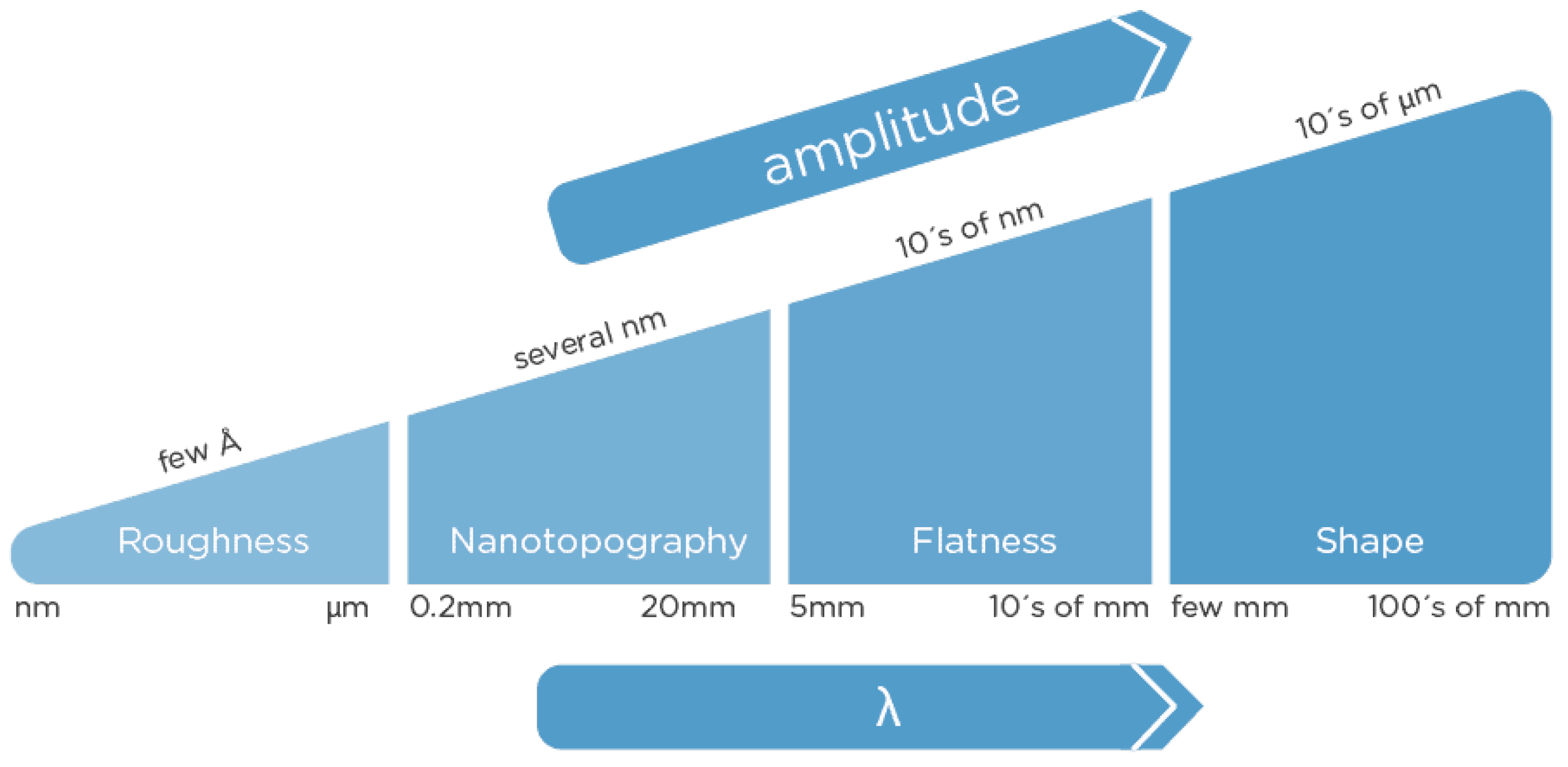
The present research focuses on studying the wavefront phase measurement technique to determine the surface profile of silicon wafers [
24]. This technique relies on capturing images in two conjugate planes of the lens. Through this method, two defocused images were obtained and used to reconstruct the phase of the silicon wafer, and consequently of its surface, by estimating the first derivative of the phase. It should be noted that this measurement technique allows for the acquisition of approximately 8 million pixels, resulting in a high lateral resolution of 65 µm and a depth resolution of less than 1 nm. Furthermore, the phase front measurement technique is noninvasive, which means that it does not require physical contact with the sample under study, making it particularly useful for analyzing fragile or delicate materials [
25,
26]. However, the technique has limitations in terms of resolution. The resolution is determined by the camera resolution used to capture the images in the two conjugate planes as well as by the optical system employed. For measuring the shape of a silicon wafer with a lateral resolution of 65 µm, a high-resolution camera with dimensions of 6388 × 6388 pixels and a pixel size of 3.78 µm is required. This translates to the need for a 30 cm field of view to cover the entire wafer surface. Achieving such high resolution entails significant costs due to the requirement for nonstandard lens sizes.
To improve lateral resolution during measurement of the nanotopography and roughness of silicon wafers, a redesign of the optical system for measurement of the surface profile is proposed using the stitching technique [
27]. The stitching technique involves combining multiple images into a single panoramic image. Overlapping images of the same sample are used to generate a panoramic image with higher resolution and a larger field of view than could be achieved with a single image. The stitching technique has previously been used with interferometry to characterize X-ray mirrors [
28,
29,
30,
31]. It has also been applied to measure the wafer profile with interferometry, achieving a lateral resolution of 40 µm, a field of view of 40 × 40 mm
2, and a measurement time of 3–4 min for a wafer of 300 mm [
32]. Another application of interferometry stitching was demonstrated by Bastian Tröger et al. [
33], who presented a tool for measuring 300 mm wafer nanotopography using white-light interferometry. They achieved a lateral resolution of 150 µm and a depth resolution of 10 nm obtained using an 85 × 85 mm
2 field of view, allowing for a throughput of approximately twenty wafers per hour.
The proposed new design of the optical system allows for improved lateral resolution with values below 10 μm in the measurement of nanotopography and roughness of silicon wafers (see
Figure 1). This leads to more precise measurements of the wafer’s surface shape. Additionally, this technique offers the advantage of reducing the costs associated with the use of nonstandard lenses for image capture, thereby increasing the accessibility of the technique for various applications.
2. Materials and Methods
As mentioned earlier, the objective of this work is to create a device capable of measuring the surface of silicon wafers using the stitching technique.
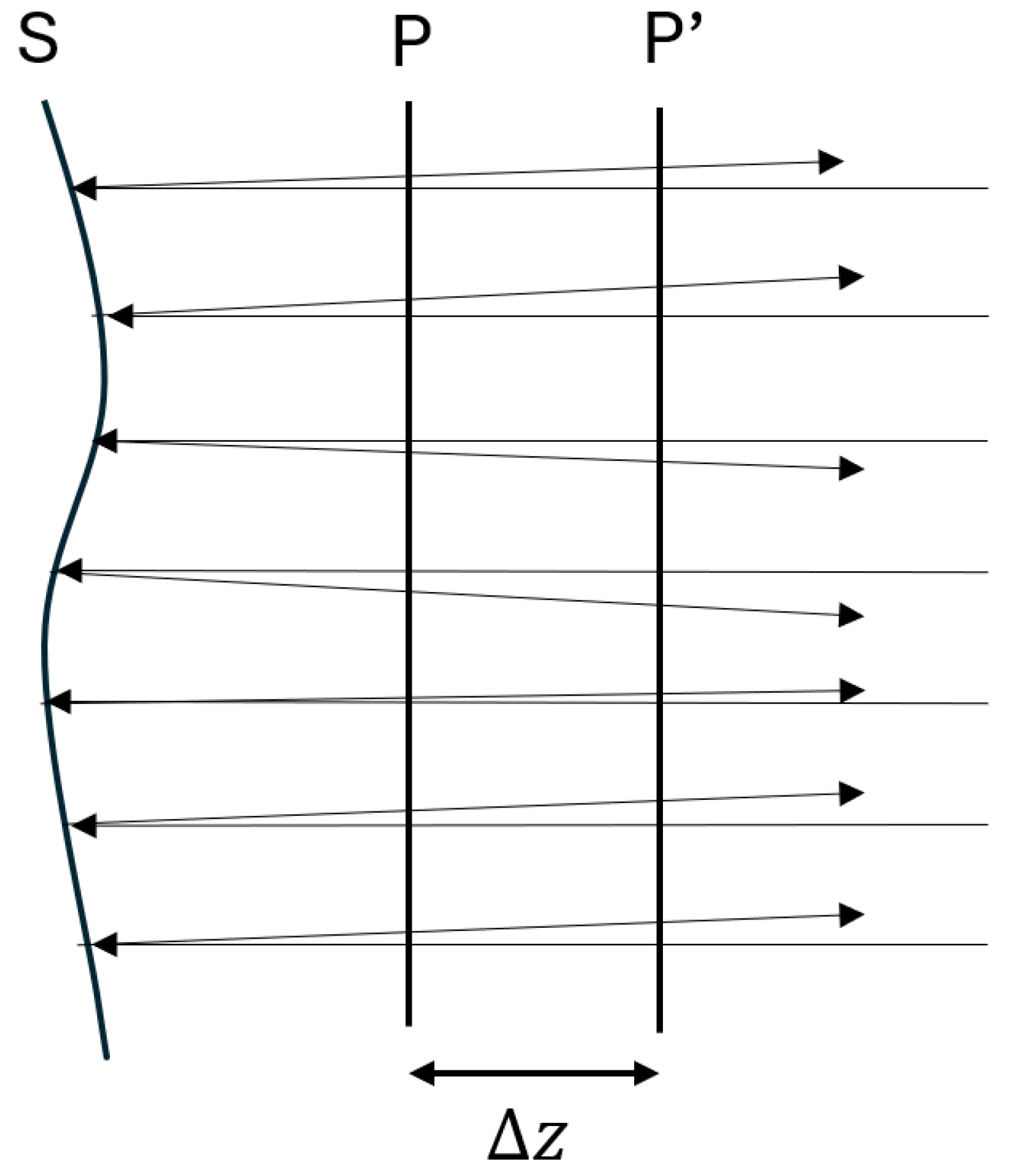
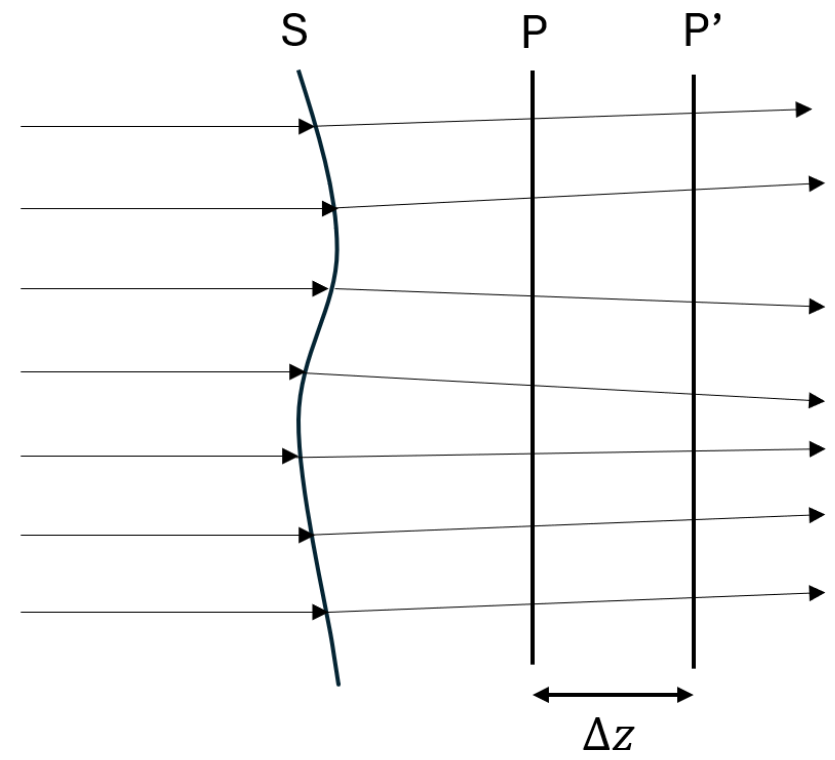
First, the most important step is to construct a wavefront phase sensor. This can be done in two ways: reflection (see
Figure 2) or refraction (see
Figure 3). The technique involves capturing two images before and after the conjugate plane with respect to the sample. Two planes within an optical system are said to be conjugate planes if the intensity distribution across one plane is an image (generally magnified or demagnified) of the intensity distribution across the other plane. Likewise, two points are said to be conjugate points if one is the image of the other.
To achieve this, a collimated beam of light is directed towards the surface of the silicon wafer. The incident light interacts with the surface, then the reflected light is captured by a camera, as said before, at two different points. The captured images are then processed using advanced algorithms to reconstruct the complete surface profile of the wafer.
The stitching technique can be used to combine multiple measurements taken from different areas of the wafer, allowing a more comprehensive and accurate representation of the surface to be obtained. This is particularly useful in applications where the surface features of the wafer exhibit variations across different regions.
Overall, the development of a wavefront phase sensor and the implementation of the stitching technique enable the creation of an apparatus capable of accurately measuring the surface of silicon wafers with high axial and lateral resolution.
2.1. Optics
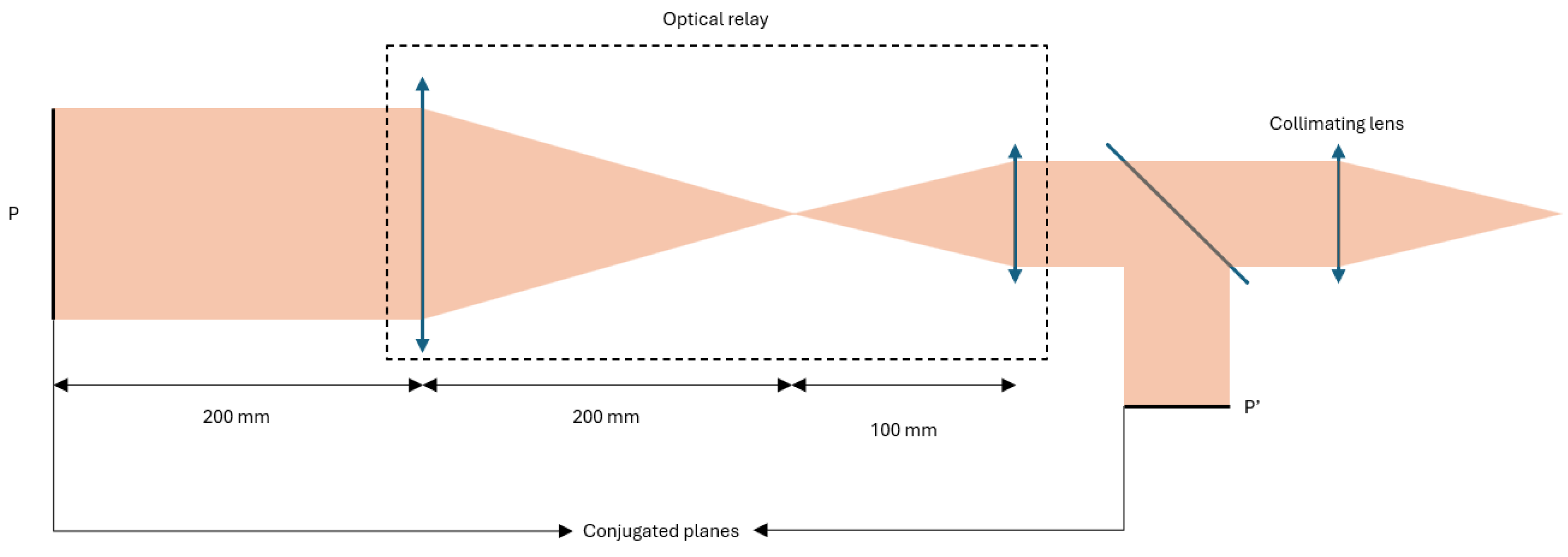
The optical part (
Figure 4) consists of a 1-inch lens with a focal length of 100 mm for the collimator. Next, the collimated light undergoes transmission through a 4f system with a magnification factor of 2, achieving a field of view with a diameter of 40 mm. The relay setup for this process involves the utilization of two achromatic lenses. The first lens is an achromatic lens with a focal length of 100 mm and a diameter of 1 inch. The second lens is an achromatic lens with a focal length of 200 mm and a diameter of 3 inches. Subsequently, the light is reflected on the silicon wafer and collected on the aforementioned conjugate planes by an
ASI6200MM Pro camera, which has a resolution of 6388 × 6388 pixels with a pixel size of 3.8 μm. With these characteristics, the theoretical lateral resolution is 7.56 μm. The light source used here is a 400 nm LED. The selection of a 400 nm LED as the light source was based on two important criteria, namely, the diffraction limit and the Fresnel distance.
The diffraction limit refers to the fundamental limitation on the ability of an optical system (such as a lens or aperture) to accurately reproduce or resolve fine details of an object or a wavefront. It is determined by the wavelength of light and the numerical aperture of the optical system. When the dimensions of the details or features in an object are smaller than the diffraction limit, they cannot be resolved separately and appear blurred or smeared together. The expression used to calculate the diffraction limit for small angles is provided by
where
is the wavelength,
d is the aperture diameter, and
is the minimum angle for two objects to be distinguishable in radians.
On the other hand, the Fresnel distance plays a crucial role in determining the distance at which the diffraction effects become significant. As mentioned earlier, it marks the point where the wavefront starts to exhibit notable changes due to diffraction. By considering the Fresnel distance, the system ensures that the propagation of light and the resulting diffraction effects are appropriately accounted for. In addition, according to [
34], the Fresnel length determines the resolution of the intensity fluctuations. Its significance is that any wave front perturbations of scale smaller than the Fresnel length are blurred and invisible to the detector. The expression is provided by
where
is the wavelength,
z is the distance between the conjugated planes, and
the size of the pixels.
2.2. Mechanics
The mechanical part consists of four different linear stages for the movement of the wavefront phase sensor in order to use the stitching technique. Two PT-GD150-300 linear stages will be used as the X-axis and will be connected together, another PT-GD150-300 stage will be used as the Y-axis and the wavefront phase sensor will be mounted on it. For capturing the two intensity images, a smaller stage, specifically the PT-GD102P(15), will be used. The distance between images, or conjugate planes, is determined by the Fresnel distance. The final design can be seen in
Figure 5.
2.3. Electronics
The stage motors are linear stepper motors. These will be controlled using an Arduino NANO microcontroller through TMC2209 drivers for the motors that move the 300 mm stages, supporting a maximum current of 3 A, and TMC2226 drivers for the motor of the 15 mm stage, supporting a maximum current of 1.5 A. Using this combination of linear stepper motors, Arduino NANO microcontroller, and TMC2209/TMC2226 drivers, the system enables precise control of stage movements, allowing for accurate positioning of the wavefront phase sensor and facilitating the desired functionality of the overall setup.
2.4. Quantitative Phase Imaging
As mentioned above, the shape of the reflective surface measures is obtained from two slightly defocused images. Both defocused images can be defined as continuous functions
and
. If a projection of these images is made in a certain direction in a Radon-like way, then this can be expressed for a given angle, as shown below.
Now, if we integrate along the
s coordinate, a cumulative distribution function (CDF) for both
and
along the given projection is obtained.
The differences observed along the ordinate axis (also referred to as histogram specification) between the two CDF curves correspond to the mean slope in the average plane between the two defocused images, as described in [
35,
36]. This relationship can be expressed mathematically using the directional derivative of the wavefront along
s:
where
and
z is the distance between the plane conjugate to the sample to one of the defocused planes. By computing this expression for all angles from 0 to
and integrating, the wavefront phase can be determined.
2.5. Residual Stress Induced During Die-to-Wafer Bonding
The utility of the measurement can be used for different purposes; one of these purposes is the in-plane distortion, which is calculated using the stress induced by the different stages that silicon wafers go through during the manufacturing process of microchips and chips in electronic devices. In this work, a method for calculating the stress induced by die-to-wafer bonding is presented. There are different methods for calculating the stress, including analytical models, finite element simulations, and calculation from wafer shape measurements [
37]. This work focuses on the latter.
The stress calculations are performed using the Stoney model, which is used to extract residual stress distributions from the wafer geometry measurements (wafer shape and thickness). In this model, it is assumed that the deformation is much thinner than the substrate, that the residual stress and thickness of the film do not vary with spatial position, and that the deformation is elastic [
37,
38].
This equation relates the residual stress in the film to the film thickness , substrate thickness , biaxial modulus of the substrate , , where and are the Young’s modulus and Poisson’s ratio of the substrate, respectively, and curvature .
To calculate the stress in the film from the shape measurement, the curvature must first be estimated. This can be accomplished by direct numerical differentiation of the shape data. To achieve accurate curvature values through differentiation, shape data must have a sufficiently high spatial resolution. In this case, the shape data have a resolution of 7.56 μm.
3. System Calibration
This section explains the calibration procedure, which is a crucial step in obtaining reliable measurements. The calibration process is performed as follows.
3.1. Main Calibration
The main calibration process involves precise adjustments of several system components to ensure accurate wavefront measurements. Key calibration steps are outlined below:
Main Lens Position: The distance between the sample and the main lens is critical for minimizing defocus. This affects the peak-to-valley values of the measured wavefront. As shown in
Figure 4, the camera and sample must be positioned at the conjugate planes of the 4f relay system for optimal performance.
Camera Position: The camera position is adjusted using the diffraction pattern of a calibration object, such as a thin wire or a patterned dice on a silicon wafer. The camera is moved back and forth until the diffraction pattern is minimized based on visual inspection.
Calibration Mirror: The calibration mirror corrects system-induced wavefront aberrations, referred to as bias. Its tip and tilt angles are adjusted to create a quasi-circular image without vignetting. The camera is then shifted iteratively to intra- and extra-focal positions, where both images are fitted to ellipses to minimize ellipticity and vignetting.
Flats: To reduce internal reflections, a servomotor-driven circular cover blocks the main lens, capturing images in intra- and extra-focal planes. These images are subtracted from all subsequent measurements to correct reflection artifacts.
Camera Temperature Stability: Maintaining a stable camera sensor temperature ensures consistent readout noise between intra- and extra-focal images. Variations in signal-to-noise ratio (SNR) can cause incorrect defocus estimation. The camera’s integrated PID control regulates sensor temperature, with future studies planned to evaluate SNR and temperature variations.
LED Temperature Stability: A stable LED temperature prevents intensity fluctuations that could distort wavefront recovery. A PID-controlled Peltier plate regulates the LED temperature throughout the measurement process with less than 0.5 degrees variations.
Room Temperature: Environmental temperature changes affect the lenses’ focal lengths, causing defocus which worsens the low order frequencies of the recovered phase. To mitigate this, the system is housed in an ISO7 temperature-controlled clean room with 0.5-degree variations. Despite this controlled environment, temperature variations may still impact measurements.
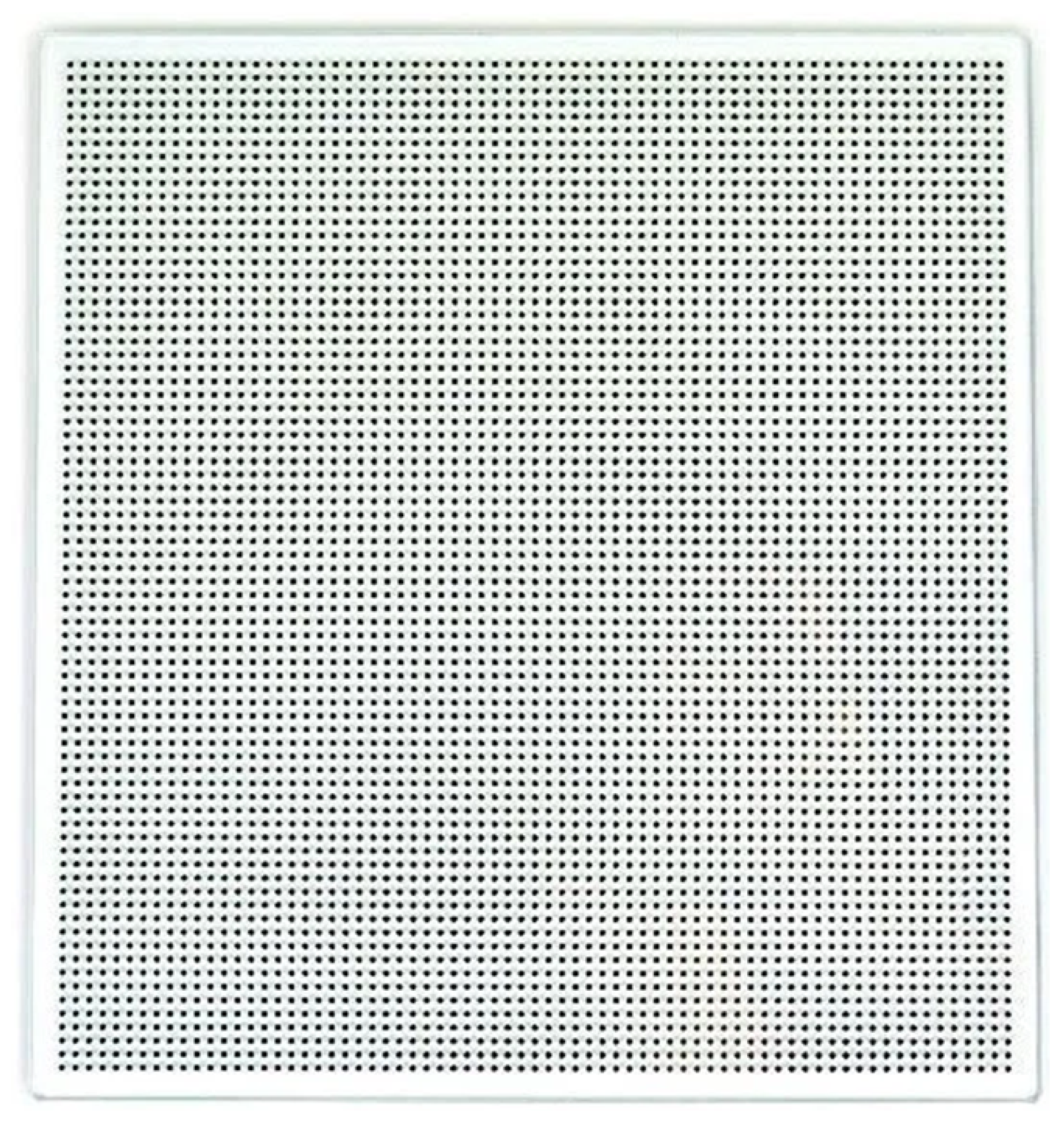
Camera Angle: The camera’s angle must be accurately adjusted for proper image stitching. This parameter is important because of the nature of the stitching technique, which supposes that there is movement between consecutive measurements. This is achieved by using a calibration mask, as shown in
Figure 6 and
Figure 7, ensuring seamless stitching between captured images.
3.2. Perpendicularity Between Linear Stages
The importance of assigning global coordinates to our measurements is crucial. In real life, achieving two perfectly perpendicular stages is difficult, and a calibration mask is needed for correction (see
Figure 7). Both the camera angle and the perpendicularity between linear stages are corrected by rotational and translation transformations of the images.
In order to correct the camera angle and perpendicularity between linear stages, a change of basis has to be performed. This change of basis consists of rotation and translation.
Figure 8 shows the required transformations. A simple change of basis is applied by using Equation (
9) to convert the measurements from the local coordinate system (x, y) to a global coordinate system (u, v).
In the above equation,
is the angle of the camera, while
and
are the number of pixels of mismatch between consecutive measurements due to stage errors and perpendicularity. First, to obtain the rotation angle, which includes the error due to the rotated camera, we calculate the largest square inscribed onto a single image of the calibration mask and transform it into a frequency space. The orientation of the repetitive pattern of the calibration mask can be easily detected. We run through different angles and check where the sums of middle horizontal and vertical lines are maximum. Second, when the images have been rotated, the common part of two consecutive images is selected. This is possible because we know the sensor pixel size, displacement, and magnification. The best way to find the values of
and
is to select the same circle in the overlapped part of both images. Later, a phase correlation is applied to the images to estimate the relative translation offset between them. The phase correlation is performed first by transforming both images into the frequency domain:
where
and
are the input images. We calculate the cross-power spectrum by taking the complex conjugate of the second result, multiplying the Fourier transforms together element-wise, then normalizing this product element-wise.
We then obtain the normalized cross-correlation by applying the inverse Fourier transform.
The peak in
r provides the values of
and
.
This transformation must be applied to all captured images before stitching is performed.
3.3. Distortion
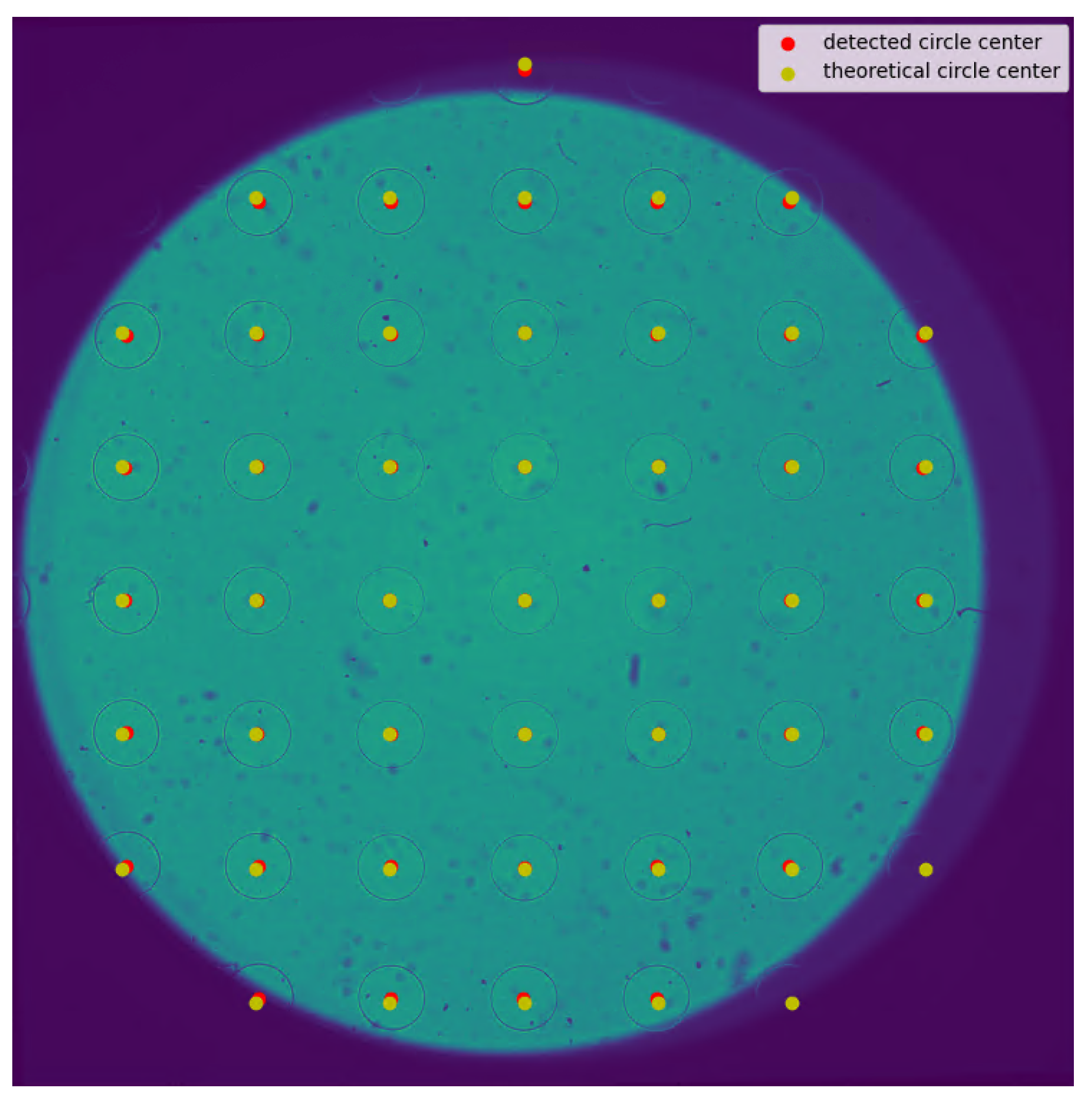
All real optical systems are affected by optical aberration, which causes distortion over the captured images. In order to estimate and correct for the distortion, a calibration mask is used. Knowing the spacing between the circles, it is possible to determine the distortion caused by the optical elements. Correcting the distortion is also a key step in correctly stitching together consecutive measurements.
First, the circles are detected in the field of view provided by the sensor. Knowing the system magnification and the pixel size sensor, it is possible to obtain the pixel size in the object plane, which in this case is 7.56 μm. With these data and the known distances between the circles of the calibration mask, it is possible to obtain the deviation of each circle from its real position, as shown in
Figure 9.
The process of creating an interpolant involves approximating the differences between the real and theoretical positions of the circles using a mathematical framework based on data triangulation and cubic interpolation. Initially, the input data points are triangulated using Qhull, a computational geometry tool that generates a non-overlapping triangulation of the points in a two-dimensional plane. This results in a mesh of triangles whose vertices correspond to the given data points.
The process of triangulating input data points using Qhull involves dividing a two-dimensional domain into non-overlapping triangles whose vertices correspond to the given data points. Mathematically, this is described as follows: given a set of points in the plane, a triangulation T is a collection of triangles such that each vertex of every triangle in T belongs to the set S. Additionally, any two triangles in the triangulation intersect only at a shared vertex or a shared edge, ensuring non-overlapping boundaries. The union of all triangles in the triangulation covers the convex hull of the set S, denoted as Conv(S).
Each triangle in the triangulation can be mathematically represented by three vertices. For a triangle
with vertices
, and
, its geometric definition is expressed as the convex hull of these points:
Qhull typically performs Delaunay triangulation, which optimizes the triangulation by maximizing the minimum interior angle of all triangles, thereby avoiding narrow elongated triangles. This criterion is achieved by ensuring that no point in the set
S lies inside the circumcircle of any triangle in the triangulation. This condition can be verified mathematically using a determinant-based test. For a triangle with vertices
, and
and a point
from the set
S, the circumcircle condition is satisfied if the following determinant is positive:
If this inequality holds for all triangles and points in the set, then the resulting triangulation satisfies the Delaunay condition. Thus, Qhull computes an optimal triangulation by ensuring that the triangles are non-overlapping, fully cover the convex hull of the points, and adhere to the Delaunay property, creating a structure suitable for smooth and efficient interpolation.
A cubic piecewise interpolation is then applied over the triangulated domain. This interpolation constructs distinct cubic polynomials for each triangle, ensuring a smooth approximation of the data. For a triangle with vertices
, the interpolating polynomial is typically expressed in the form
where the coefficients are determined through interpolation constraints.
To achieve a smooth representation across the entire domain, the interpolation within each triangle is represented using a Bezier polynomial defined in barycentric coordinates. The Bezier representation takes the form
with the control points determined by the interpolation process.
To ensure continuity of both the function and its first derivatives across the triangle boundaries, the Clough–Tocher scheme is employed. This method subdivides each triangle into three smaller sub-triangles, enforcing interpolation constraints that maintain smoothness across the entire domain. The resulting interpolant provides a continuous and differentiable approximation of the data, effectively capturing the discrepancies between real and theoretical circle positions [
39]. The interpolant is guaranteed to be continuously differentiable.
The gradients of the interpolant are chosen so that the curvature of the interpolating surface is approximately minimized. The gradients for this are estimated using the global algorithm described in [
40,
41].
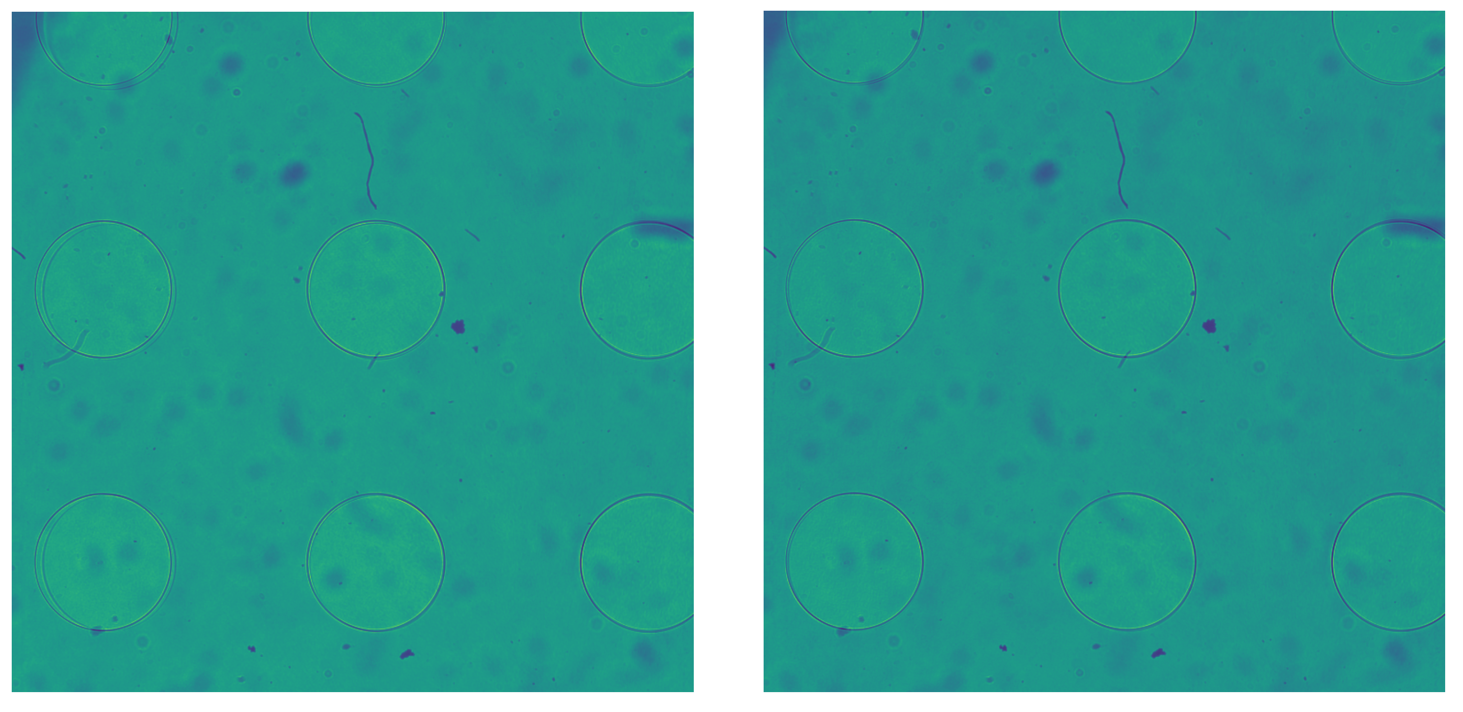
Figure 10 shows the difference between two overlapped images with and without distortion correction. It is worth noting that after distortion correction, the circles match better than without correction, as in the latter case only the inner circles are matched because the system aberration is larger at the edges of the field of view.
3.4. Stitching Technique
After the calibration process and distortion correction, the measured sample can be composed using the stitching technique. The stitching technique consists of combining two consecutive measurements while taking into account the pixel size of the camera, the magnification of the system, the displacement between measurements, and the correction of perpendicularity between the linear x-axis and y-axis linear stages. Knowing these values, it is possible to combine both measurements with a sigmoid function; this makes the overlapped zone of two consecutive measurements continuous, acting like a weighted sum. The common part of both images is defined as follows:
where
c and
f are the first and last pixels taken on the x-axis for the first and second images, respectively. If
is the first input image and
is the last, then their domain in the common part of the images is
Then, as said before, the common part of the composed image is a weighted sum along the x-axis using a sigmoid function:
where
is a common sigmoid function, as seen in Equation (
23). Because the sum of both sigmoid functions is 1 in the full domain where it is applied, there is no inconsistency between the intensity values in the resulting stitched image.
Thus, the final image is the concatenation of the first image without the common part of both measurements, the weighted sum of the common part, and the rest of the image of the second image without the common part.
Repeating this technique iteratively allows a full row to be combined with the same process. Using the same technique, it is also possible to combine two consecutive rows. In the following chapter, a full measurement is shown.
4. Results
A quarter-wafer sample from IMEC was utilized, with die-to-wafer bonding applied to specific regions of the wafer. A notable result of this work is to determine the shape (bow/warp) of dies that are thinned and then glued onto a carrier wafer, along with the resulting deformation.
First, 196 images were taken in both defocused planes (see
Figure 11). The full capture process is shown in
Figure 12. After both stitched measurements were obtained, the quantitative phase algorithm was applied to obtain the shape of the wafer, as explained in the previous section.
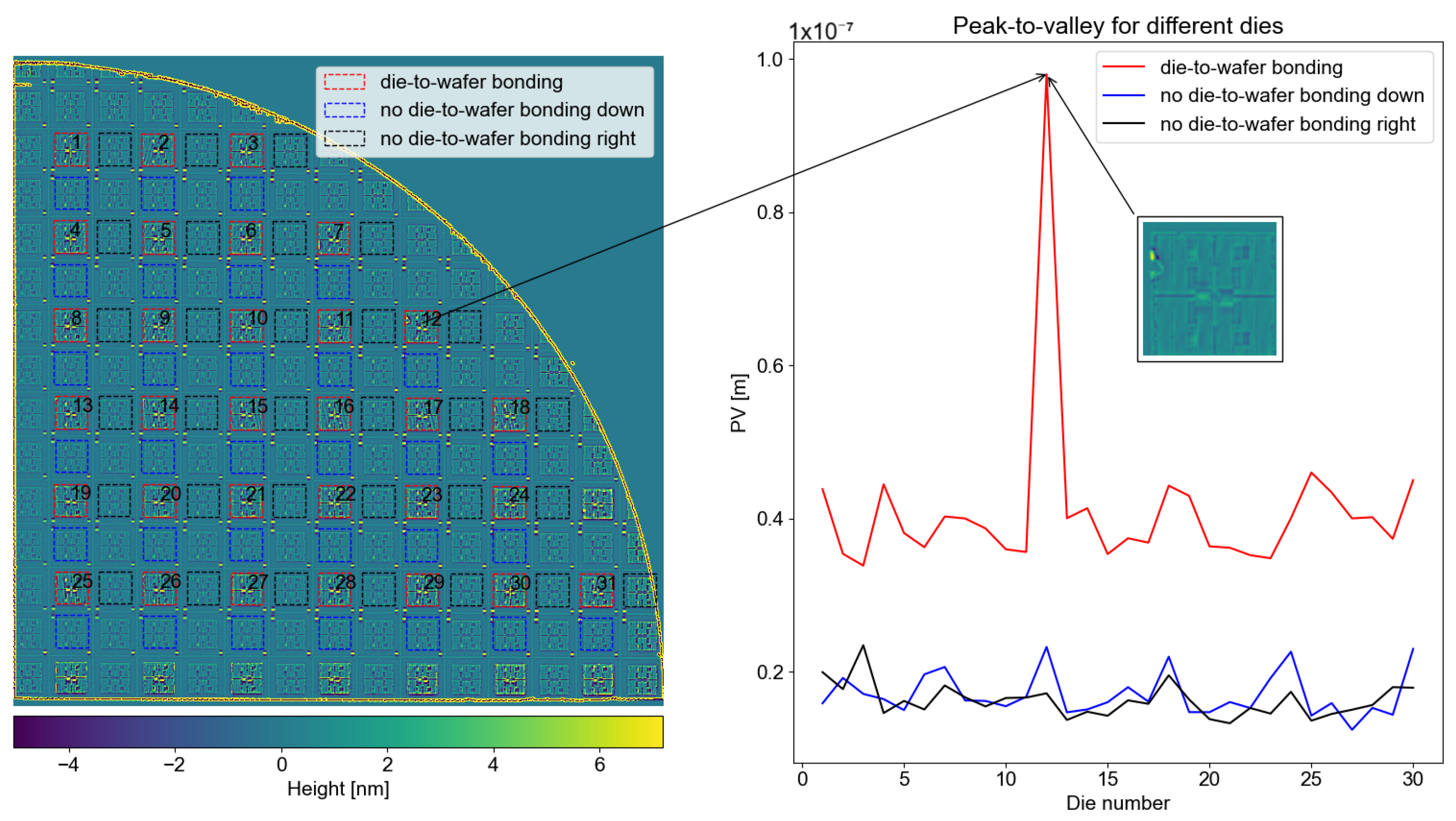
In
Figure 13, it is possible to see the peak-to-valley difference between both types of die; die-to-wafer bonding is around 2.5 μm, while non-die-to-wafer bonding is around 1.8 μm. In addition, it is worth analyzing the full measurement in order to check whether all die-to-wafer bonding dies have higher peak-to-valley values than for non-die-to-wafer bonding.
Figure 14 shows a full measurement of a quarter of the wafer. In the same figure, both types of die are selected and numbered. To maintain consistency, each die-to-wafer bonding die is compared with its neighboring non-die-to-wafer bonding dies, positioned directly below and on the right of it, as depicted in the figure. From the same figure, it is evident that all die-to-wafer bonding dies exhibit greater deformation compared to the non-die-to-wafer bonding dies. Note that the global shape of the wafer affects the peak-to-valley, as expected. A similar comparison is presented in
Figure 15, this time with the application of a high-pass filter to the original data. The use of a high-pass filter allows for the isolation of higher-frequency surface variations by removing long-wavelength features, making localized deviations more prominent. The high-pass filter used here is a double Gaussian filter which is defined in the SEMI Standards [
42]. This filter can be expressed as follows:
where
is the cutoff frequency. The cutoff frequency used in
Figure 15 is 200 μm.
As a result, it can be seen that the die-to-wafer bonding dies exhibit a noticeably higher peak-to-valley, suggesting increased surface irregularities or deformation after bonding. Furthermore, the high-pass filtering reveals a small defect on one of the dies. It is very interesting that different columns of dies exhibit different peak-to-valley patterns. For example, it can be seen from the two figures mentioned above that the first column, which includes dies 1, 4, 8, 13, 19, and 25, has higher peak-to-valley than the column with dies 2, 5, 9, 14, 20, and 26.
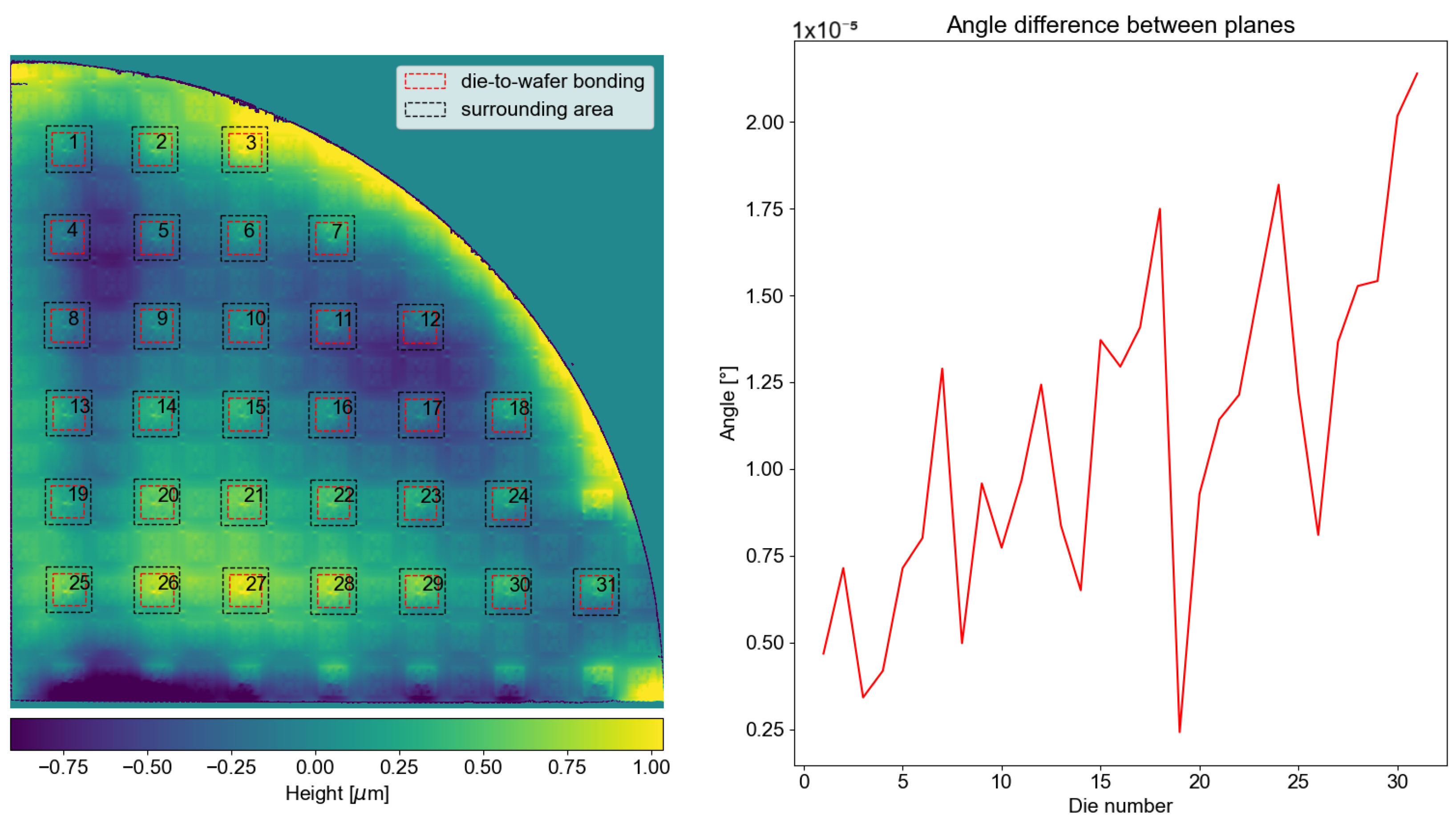
Continuing with die analysis, a very important parameter in the industry is the coplanarity between the die-to-wafer bonding and the surrounding area.
Figure 16 shows the difference between the best fit plane of the die-to-wafer bonding (area of the red dashed line) and the surroundings (area between the red and black dashed lines). The angle differences between both planes are on the order of microdegrees.
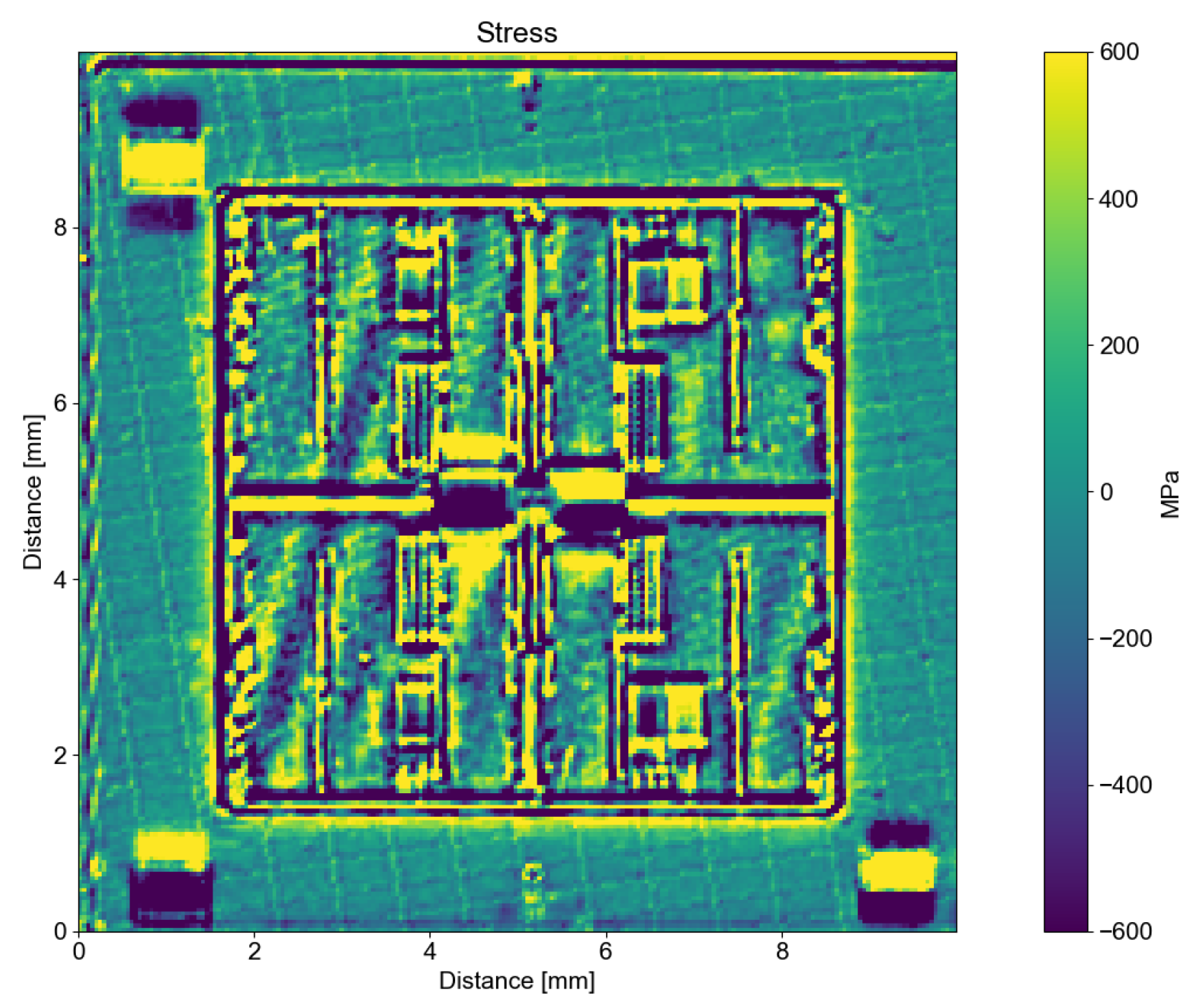
Lastly, one of the most interesting results is provided by the stress induced during die-to-wafer bonding. Process-induced overlay errors are a growing problem in meeting the ever-tightening overlay requirements for integrated circuit production. By calculating the stress, the overlay error can be minimized. In
Figure 17, the stress produced by a film deposited over a die has been calculated using the Stoney equation, which, as said before, is valid if the film is much thinner than the substrate, the residual stress and thickness of the film do not vary with spatial position, and the deformation is elastic. Taking this into account, and considering that the wafer and film were assumed to be elastic and isotropic, the residual stress in the film was calculated using Equation (
8). Note that the discontinuities of the die-to-wafer bonding cause some artifacts that strongly affect the scale of the plot; nonetheless, in the inner part of the die, where some wavy artifacts caused by the bonding can be seen, the values are on an order of magnitude of hundreds of MPa. These are typical values for induced stress in thin films over silicon wafers, as shown in [
37]. Lastly, the curvature obtained from the direct differentiation of the shape obtained by the machine in Equation (
8) is the delta shape between a die with die-to-wafer bonding and a die without it, as the required value is the stress induced during the process.
5. Conclusions
The shrinking size of electronic devices has driven an urgent demand for advanced metrology techniques capable of high-resolution and high-throughput inspection of silicon wafers. In this work, we introduce an advanced wavefront phase sensor that demonstrates exceptional metrological performance. The system achieves sub-nanometer axial resolution, specifically below 1 nm, and lateral resolution around 7.56 μm across diverse silicon wafer samples. Such precision is critical for addressing key industry challenges, including defect detection in die-to-wafer bonding, coplanarity measurement, and residual stress analysis from thin-film deposition processes. These functionalities are vital in ensuring the structural integrity, operational reliability, and extended lifespan of semiconductor devices while mitigating risks of device failure and performance degradation.
Our proposed system surpasses traditional interferometric methods by utilizing a partially coherent light source, which significantly enhances vibration tolerance. This represents a critical advantage in industrial environments prone to mechanical disturbances.
Future research will address throughput optimization by investigating techniques for image overlap correction through advanced stitching algorithms, enabling seamless coverage of larger wafer areas. Additionally, an automated interchangeable lens system integrated with a precision linear translation stage is under development. This mechanism will allow for dynamic adjustment of focal lengths and pixel sizes, further enhancing the system’s versatility and applicability to a wider range of inspection tasks.
It is worth mentioning that the stitching process is performed on intensity images rather than on the final phase data. As a result, system-induced aberrations, referred to as bias, remain in the stitched output. This leads to inaccuracies in low-order frequencies; for this reason, the presented data are shown with the second-order polynomials removed. In future work, a method for mitigating this inaccuracy will be studied.
In conclusion, our proposed system represents a significant advancement in silicon wafer metrology. Its unique features position it as a promising solution for next-generation semiconductor manufacturing, offering precise, efficient, and scalable inspection tailored to evolving industry demands.


