1. Introduction
Precision Measurement Technology [
1] is a package that supports semiconductor chips (such as wafer bonding precision control [
2]), MEMS [
3] device performance testing (such as micro-actuator displacement calibration [
4]), and ultra-precision machining equipment with the feature size of integrated circuits entering into 7 nm and below. The triple demand of “high precision (submicron and below), high robustness, and low cost” for displacement measurement in industry is increasingly urgent. However, the contradiction between accuracy, environmental adaptability, and cost of current mainstream measurement technology is difficult to reconcile, resulting in most high-end solutions being limited to laboratory scenarios, while low-cost solutions are difficult to meet the accuracy requirements, forming a “measurement technology bottleneck” in the field of advanced manufacturing.
At present, the micro-displacement measurement methods have formed a pattern of coexistence of multiple technical paths, but each method has significant differences in accuracy, environmental requirements, cost, and engineering applicability, such as laser interferometry [
5] based on the Michelson interference principle, which can achieve nano-scale (0.1~10 nm) resolution, and is the standard of high-precision laboratory measurement. But it depends on a high-purity He-Ne laser [
6], a precision optical lens group, and a strict vibration isolation system; the total cost of the whole set of equipment is generally more than CNY 100,000, and complex operation requires professionals to use. At the same time, this method is sensitive to environmental vibration and dark room, air refractive index, completely unable to adapt to workshop-level complex working conditions, can only be used in an ultra-clean laboratory at constant temperature and humidity, and cannot be applied on a large scale. The optical fiber sensor [
7] based on the principle of interference and refraction of light is more resistant to vibration than laser interferometry, can suppress the influence of temperature, and is applicable to a wider range of environments than laser interferometry, with a resolution of 0.5~5 μm. However, its core shortcomings lie in the complexity of optical path calibration, high debugging cost, and easy loss of optical fiber probes. It is difficult to achieve large-scale deployment of multiple measurement points. There are also piezoelectric ceramic driving methods [
8] that convert voltage signals into micro-displacements by using the “inverse piezoelectric effect [
9]” of piezoelectric materials. The resolution can reach the sub-nanometer level, and the response speed is fast. However, piezoelectric ceramics have inherent “hysteresis nonlinearity [
10]” and “creep characteristics [
11]”, and, even if PID closed-loop feedback control is adopted, it is still necessary to additionally design complex error compensation algorithms. In addition, high-precision piezoelectric ceramic drivers have high unit prices, the cost of supporting control modules exceeds CNY 50,000, and the measurement range is limited.
In view of the above, the optical method environment requirements are strict and high cost, the pressure point material range is limited, and other bottlenecks. Consider that the traditional capacitive sensor has the advantages of non-contact measurement, strong anti-electromagnetic interference ability, and strong environmental adaptability, but the accuracy is limited to 0.1~30 μm [
12], and the accuracy is easily affected by parasitic capacitance [
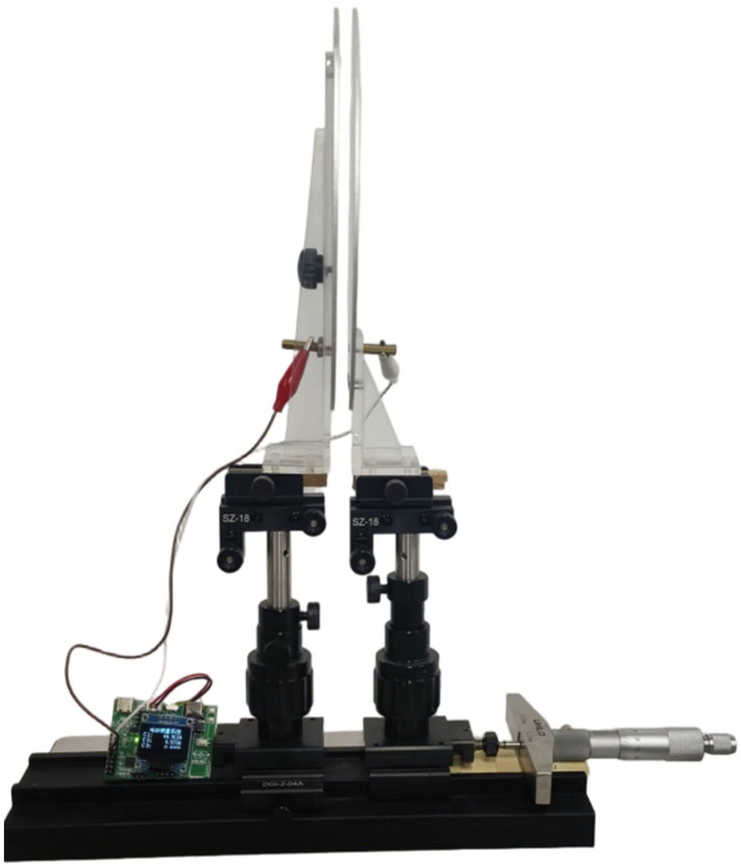
13] and other errors. Based on the idea of “optical–mechanical–electrical collaborative optimization”, a new method of micro-displacement measurement based on the parallel plate capacitance principle is proposed in this paper. Through the deep fusion of mechanical structure optimization, high-resolution hardware design, and error separation algorithm, the measurement goal of “high resolution, low cost, and wide range” is realized. The dynamic parallel calibration of the polar plate is realized through the optical-bench [
14] micrometer mechanical coupling mechanism, wherein the return clearance and inclination error of the traditional slide rail structure are eliminated, the sub-millimeter displacement of the polar plate is realized, and the cost and the limitation of small range of the polar plate displacement by using the stepper motor [
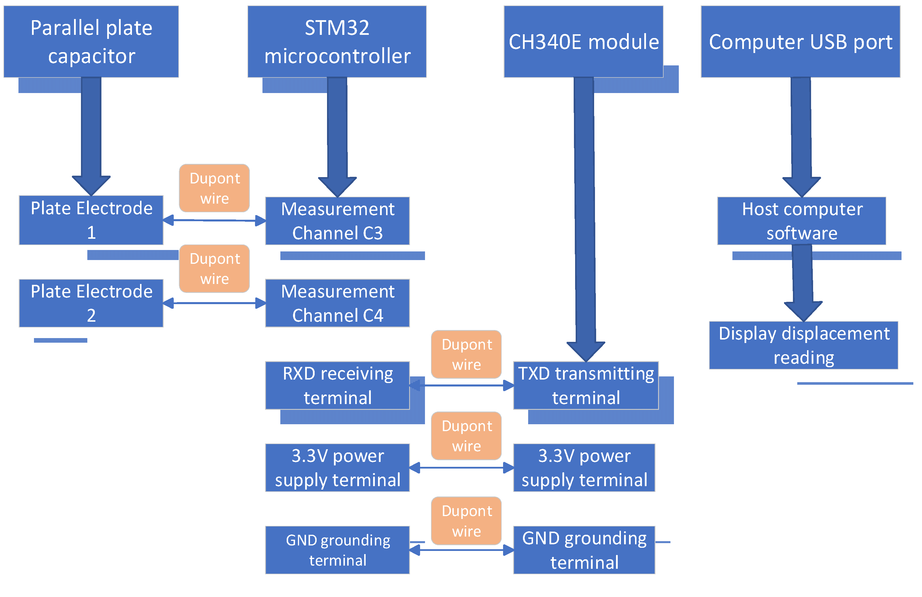
15] and the like are greatly reduced. The precision of the 21-bit high-resolution capacitance detection module constructed by the STM32-PCAP01 chip [
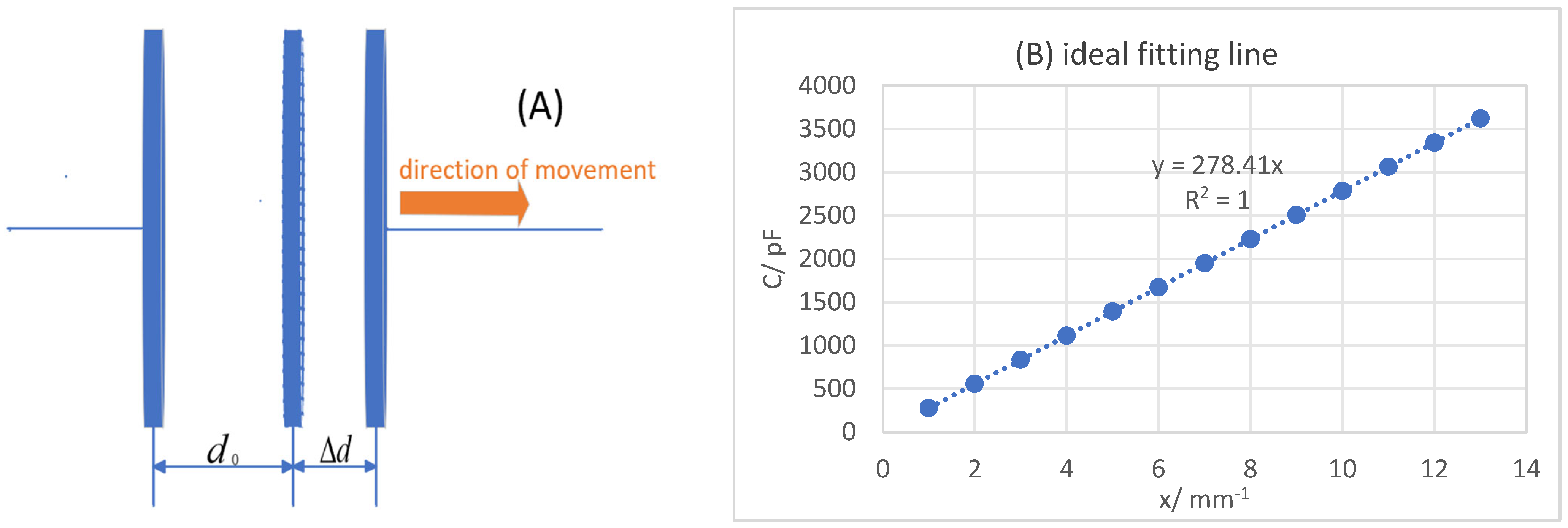
16] is 0.001 pF. Based on the charge transfer principle, the module compares the charge–discharge time ratio of the measured capacitor with the reference capacitor to detect the small capacitance change, compensates for the temperature drift, and has strong electromagnetic interference ability and environmental adaptability. A complete micro-displacement measurement system is researched and constructed. The complex nonlinear fitting model [
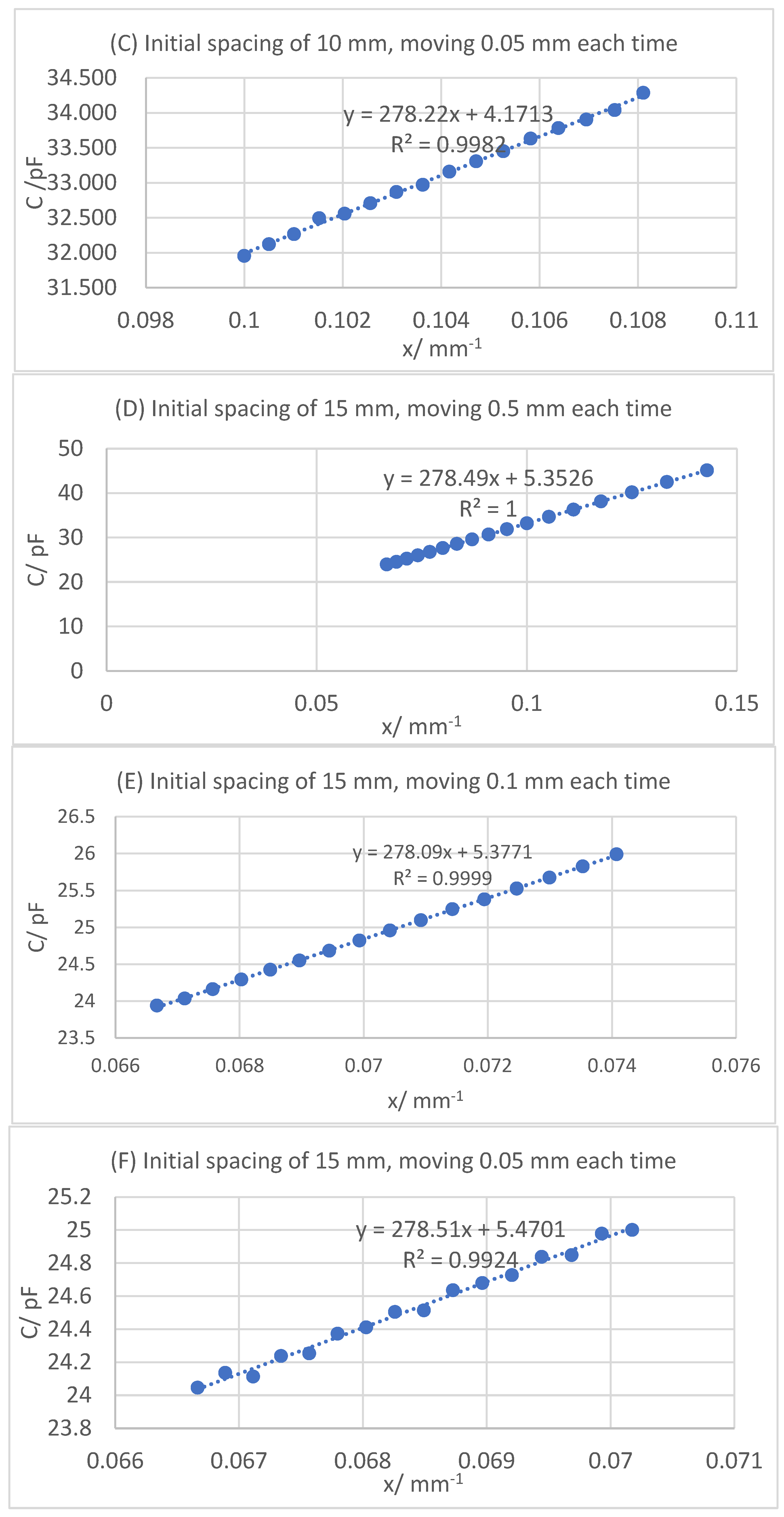
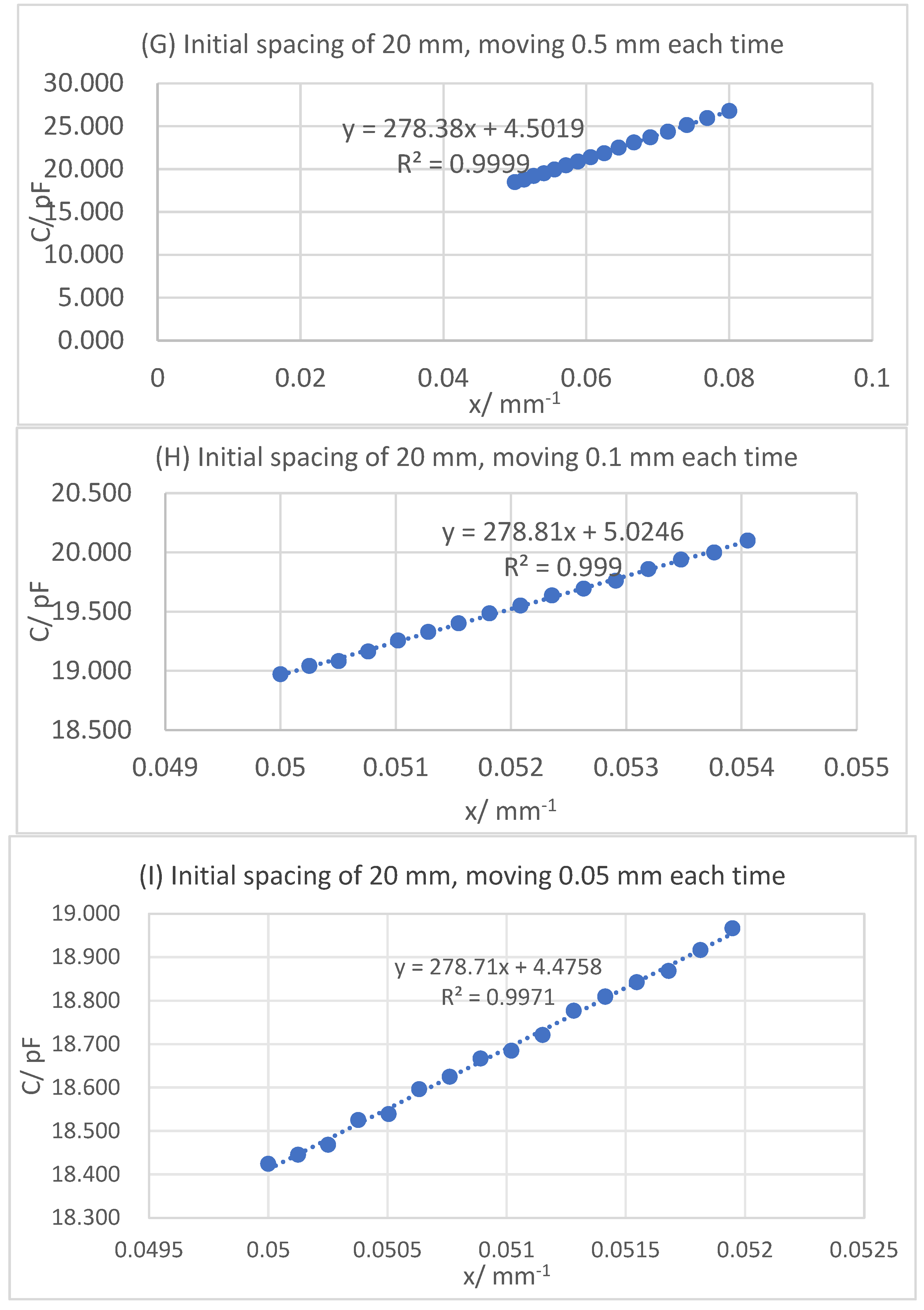
17] of data is not directly based on the inverse relationship between parallel plate capacitance and displacement, but the experimental data is processed by the linear fitting [
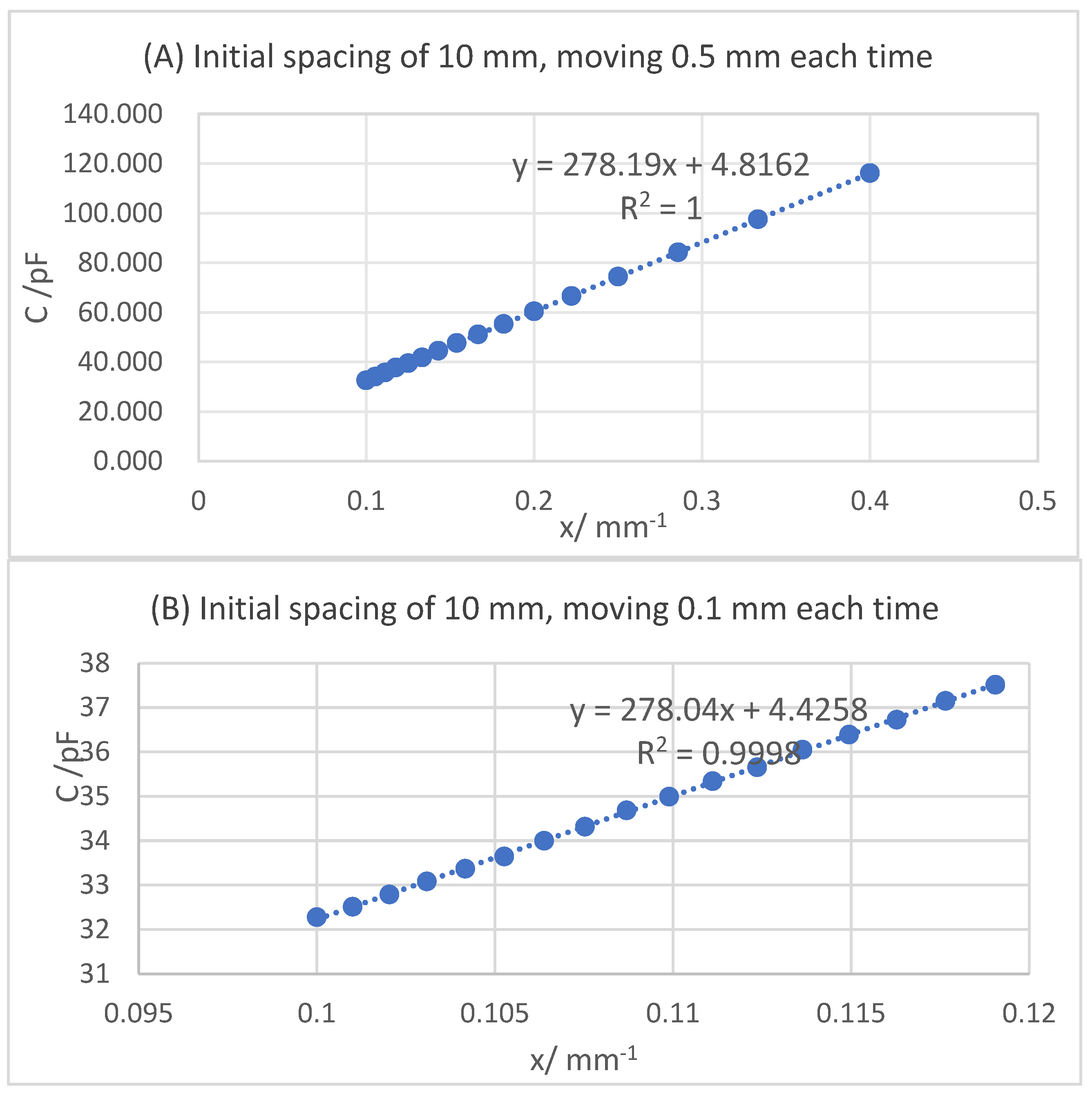
18] method, and the physical quantity of the system is effectively calibrated again. The calibration under multiple working conditions [
19] can cover different use scenarios, avoiding the problem of “high local accuracy and low global accuracy” caused by a single calibration. System calibration also effectively reduces random errors caused by different environments and initial states. The slope and intercept of a linear system have definite physical analysis meaning. The slope of linear fitting can be directly related to the sensitivity of the system. The intercept can effectively separate the errors of parasitic capacitance of the system. Through software design calibration, the pain point of “parasitic capacitance cannot be quantified” of the traditional capacitance sensor is solved, and the capacitance measurement error is remarkable.
4. Conclusions
In order to solve the bottleneck problems of traditional micro-displacement measurement technology, such as poor environmental adaptability, high cost, and low resolution, a set of capacitive sensing micro-displacement collaborative measurement system based on optical–mechanical–electrical collaborative optimization is successfully designed and built, featuring the advantage of low cost (less than CNY 600). The optical-seat micrometer coupling mechanism realizes the dynamic parallel calibration of the polar plate and effectively eliminates the mechanical return gap error; the high-resolution capacitance measurement module enhances the stability of the reading and improves the displacement measurement resolution; and the linear fitting algorithm effectively separates the parasitic capacitance, enhances the robustness of the measurement data, and can compensate the interference caused by the system error in real time. The system has been experimentally validated for micro-scale displacement and demonstrates theoretical potential for achieving nanometer-level displacement resolution based on its hardware parameters. The research system provides cost-effective solutions and application prospects for semiconductor chip packaging (avoiding mechanical probe scratching wafers), MEMS device resonance detection (relative error less than 2.5%), and ultra-precision machine tool compensation, especially in the field of industrial field and educational demonstration scenarios. Its optical–mechanical–electrical collaborative framework offers a new paradigm for the development of intelligent sensors. Future work will focus on comparative studies with high-precision benchmarks to comprehensively evaluate its measurement accuracy and systematically test its environmental adaptability.
