Abstract
The widespread adoption of fifth-generation Reduced Instruction Set Computing (RISC-V) processors in embedded systems has driven advancements in domestic processor design. However, research on processor performance optimization methods predominantly focuses on two- to three-stage pipeline architectures, with relatively few studies addressing complex five-stage pipeline processors. This study addresses this gap by analyzing optimization strategies for a five-stage pipeline processor architecture. Key areas examined include RISC-V jump instruction branch prediction (speed optimization), memory structure (memory access and resource optimization), and data-correlation-based division operations (fetch optimization). The processor core underwent CoreMark benchmark testing via a Field Programmable Gate Array (FPGA), analyzing the impact of optimizations such as branch prediction and cache on processor performance. The final processor achieved a CoreMark score of 2.92 CoreMark/MHz, outperforming most open-source processors and validating the effectiveness of the optimization strategies.
1. Introduction
With the rapid advancement of microelectronics and integrated circuit technologies, embedded processors have gained widespread adoption across telecommunications systems, industrial control, medical devices, consumer electronics, and smart home applications due to their significant advantages of compact size, high energy efficiency, and exceptional flexibility [1,2]. In the embedded computing domain, the ARM architecture has evolved over many years into a highly mature ecosystem. However, these traditional processor architectures are constrained by patent protections, requiring developers to pay substantial licensing fees for patents and architecture usage. Furthermore, due to their early development, these architectures have grown increasingly complex in design and struggle to adapt to diverse application demands. They lack a unified instruction set architecture capable of meeting the modern semiconductor industry’s requirements for customization, differentiation, and high performance [3,4,5,6]. In recent years, the RISC-V architecture has rapidly gained prominence in the industry due to its open instruction set and streamlined design philosophy [7,8]. Compared to the ARM architecture, RISC-V demonstrates significant potential in power consumption control, instruction set scalability, and ecosystem flexibility, and is gradually being adopted in critical fields such as embedded systems and the Internet of Things [9]. As an emerging instruction set architecture, RISC-V offers numerous advantages, such as modular design, streamlined instruction set, full open-source nature, and high scalability [10,11,12]. These advantages enable users to flexibly develop and customize solutions according to specific requirements. As the RISC-V software ecosystem continues to mature, an increasing number of enterprises and research institutions are adopting the RISC-V architecture for processor development. For example, in 2015, SiFive launched the first customizable RISC-V SoC platform, FreedomE300 [13], and in 2016, introduced a specific SoC named Freedom E310 SoC [14], configured based on the Freedom Everywhere E300 platform. The Freedom E310 SoC was the first commercially available RISC-V-based SoC. To date, SiFive’s standard cores remain the most widely adopted RISC-V solutions globally across multiple sectors. In July 2020, the National University of Defense Technology unveiled achievements from its “One Student One Chip (ysyx)” plan initiative: five undergraduates independently designed a 64-bit RISC-V processor, completed SoC assembly, achieved production manufacturing, and successfully ran the Linux operating system on the SoC [15]. These accomplishments fully demonstrate the immense potential of the RISC-V architecture in embedded and high-performance computing domains.
Therefore, this paper focuses on optimizing processor architecture at the hardware level and precisely quantifies the actual performance gains achieved by various optimization strategies.
Our research has contributed to the following areas:
- Optimized the design of an open-source embedded RISC-V processor, achieving significant performance gains that validate the effectiveness of the optimization methodology.
- Quantitatively evaluated each optimization technique using CoreMark benchmarking, providing a clear demonstration of the contribution level of each optimization measure.
The organizational structure of this paper is as follows. Section 2 first outlines the current state of processor design development and analyzes its primary shortcomings. Based on this foundation, it presents the optimization approach and overall methodology adopted in this paper for processor performance enhancement. Section 3 will provide a detailed description of the five-stage pipelined processor architecture based on a hardware platform adopted in this paper, systematically detailing key performance optimization strategies spanning pipeline architecture, branch prediction mechanisms, and caching. It also explains the specific optimization designs and implementations for each module. Section 4 presents optimization results for the branch prediction module, division unit, and cache module, quantifying the actual performance gains achieved by each method through comparative analysis. Finally, Section 5 summarizes the research findings and outlines potential future research directions.
2. Related Work
Current research on RISC-V processors, both domestically and internationally, primarily focuses on the design and implementation of 2 to 4-stage pipeline architectures. For instance, Reference [16] uses the AHB bus as the on-chip interconnect bus to design a 2-stage pipelined processor supporting the RV32IMAC instruction set. Reference [17] designed a three-stage pipelined RISC-V processor based on the RV32I instruction set, employing static prediction BTFN technology to handle branch conditions during pipeline execution. Reference [18] designed a three-stage pipelined processor supporting the RV32I basic instruction set, primarily describing the design and implementation of its control unit. Reference [19] addresses the demand for small footprint, low power consumption, and high performance in processors for embedded IoT devices by proposing a three-stage pipeline architecture supporting the RV32IM instruction set, featuring sequential issuance, out-of-order execution, and out-of-order write-back. Reference [20] proposes a low-power four-stage pipeline RISC-V processor supporting RV32IM instructions. Research indicates that most of the above literature focuses solely on two-to-four-stage pipeline designs. Branch handling often relies on static prediction BFTN (Backward Taken, Forward Not-taken) techniques, with limited quantitative analysis of processor performance. Research on high-performance RISC-V processors with five-stage pipelines is also relatively scarce, with few case studies [21,22] available. Most designs focus primarily on implementation, with limited performance evaluation and a lack of quantitative assessment of processor optimization strategies.
In modern processor design, pipelining technology is one of the key methods for enhancing performance. A five-stage pipeline significantly improves instruction throughput by dividing the execution process into five phases: fetch, decode, execute, memory access, and write-back [23]. The introduction of caches effectively reduces processor latency when accessing main memory, improving the efficiency of instruction and data access [24]. Branch prediction technology, meanwhile, minimizes pipeline stalls caused by control speculation, further enhancing processor execution efficiency [25].
Against this backdrop, this paper optimizes and implements a five-stage pipeline processor based on the RISC-V instruction set architecture, integrating it into a system-on-chip (SoC). The processor supports the RV32IMZicsr instruction set, adopts a classic Harvard architecture, incorporates independent instruction and data caches, and implements a dynamic branch prediction mechanism to optimize pipeline performance. In the SoC architecture design, a custom bus protocol ensures efficient data exchange between the processor and peripheral modules. To objectively evaluate the processor’s performance, the CoreMark benchmark suite is employed for comprehensive performance assessment. Crucially, this paper thoroughly analyzes and quantifies the specific performance gains contributed by different optimization techniques, providing a clear demonstration of the effectiveness of each optimization measure.
3. Processor Microarchitecture and Division Optimization
3.1. Hardware-Based Five-Stage Pipeline RISC-V Processor
The RISC-V instruction set architecture (ISA) adopts an open, free, and open-source model, featuring a simple design, flexible scalability, and high customizability. It also eliminates complex mechanisms such as condition flags and branch delay slots [26,27]. These characteristics enable users to independently customize and optimize the instruction set according to specific application requirements.
The hardware architecture of RISC-V adopts a three-operand and store-and-fetch design paradigm. Its instruction set architecture comprises an essential core instruction set, a series of standardized optional extensions, and reserved space for user-defined extensions [28]. The processor implemented in this paper can execute the RV32I core instruction set and the Zicsr extension instruction set.
To enhance performance and efficiency, we optimized the architecture based on a well-known processor, resulting in a new RISC-V processor. Longer pipelines typically require more physical resources to support [29]. Balancing performance and resource consumption, this paper first upgrades the original processor’s three-stage pipeline architecture to a five-stage pipeline architecture. This fully leverages the parallelization advantages of pipeline technology, significantly improving the processor’s instruction throughput. Second, a branch prediction module was introduced to accelerate the execution efficiency of jump-type instructions. Concurrently, a branch prediction correction module was added. When branch prediction errors occur, this correction module promptly flushes the contents of the fetch and decode stages, ensuring the correctness of processor functionality. Furthermore, the addition of a cache memory access module effectively enhances the processor’s memory access speed. Regarding the division module, this paper implements an optimization: when the source register of the subsequent instruction following a division instruction does not conflict with the source register of the division instruction itself, the division module can continue its operation. The processor can then proceed with fetching and executing instructions, further improving the processor’s instruction fetch efficiency. Finally, the improved processor is named SHriscv.
3.2. Introduction to the SHriscv Processor
The processor employs a classic five-stage pipeline consisting of fetch, decode, execute, memory access, and write-back stages. The fetch stage, as the first pipeline stage, loads instructions from the instruction memory based on the PC (Program Counter) value and passes them to the If_Id module. To enable rapid, continuous instruction loading, a branch prediction module is integrated into the fetch stage’s microarchitecture. The second stage is the decode module, tasked with decoding instruction information and transferring it to the Id_Ex module. In the third stage, the execute module selects the appropriate execution unit based on the instruction type and passes the obtained result to the Ex_Mem module. The Ex module also incorporates branch prediction result comparison, pipeline interrupts and flushes, and CSR (Control and Status Register) status register writes. The fourth stage is the memory access module. For store/load instructions, memory access operations are performed via the read/write control unit accessing the data memory. For non-memory access instructions, the data remains unchanged and is directly passed to the Mem_wb module. Finally, the fifth stage is the write-back module, responsible for writing the final result back to the general-purpose register. Figure 1 presents the main architectural components of the SHriscv processor and their interconnections. The description of each module in the SHriscv processor is shown in Table 1.
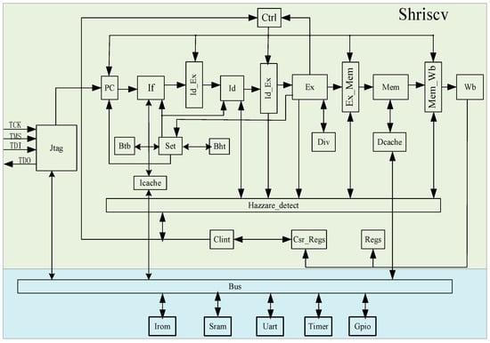
Figure 1.
SHRiscv processor architecture diagram.

Table 1.
Introduction to the various modules of SHriscv.
3.3. Processor Performance Optimization
In the TinyRISCV prototype processor, the three-stage pipeline architecture means that the branch prediction module, execution module, memory access module, and division calculation module significantly impact the processor’s clock speed, execution velocity, and execution time. Therefore, this paper focuses on optimizing these modules to enhance processor performance.
Statistics indicate that branch instructions constitute approximately one-sixth of all program instructions [1]. These control-flow instructions determine the execution path of a program. If the jump direction must be determined only in the later stages of the pipeline each time, a large number of invalid instructions will enter the pipeline. Since invalid instructions consume processor resources and introduce additional overhead, they are typically converted into no-op (NOP) instructions through pipeline flush operations. An increase in the number of no-op instructions means fewer effective processor cycles, significantly impacting overall performance. Introducing a branch prediction mechanism allows the processor to anticipate the direction and destination of conditional jump instructions in advance. This enables earlier fetching of the next instruction to be executed, thereby reducing pipeline flush frequency, shortening processor execution time, and improving system throughput.
Second, the division calculation module consumes 33 clock cycles. During this process, the pipeline pauses to await the division result, causing processor resource wastage. If data dependency checks are performed on the current and subsequent instructions during this wait, and if the division result is not required by the following instructions, fetching and executing subsequent instructions can proceed. This allows the divider to continue operating as a separate module, enabling simultaneous execution of the processor and divider to improve processor efficiency.
Additionally, the prototype processor employed a three-stage pipeline architecture, integrating execution, memory access, and write-back into a single module. This excessive logical stage depth reduced the cycles per instruction (CPI). This experiment modified it to a classic five-stage pipeline, dedicating separate stages to execution, memory access, and write-back. This fully leverages pipeline technology characteristics, increasing processor instruction throughput.
Finally, the cache serves as a buffer and accelerator between the processor and external devices, making it an indispensable component in modern computer systems. Direct interaction between the processor and peripherals would require hundreds of clock cycles. Incorporating a cache reduces the number of clock cycles needed for processor memory access, thereby enhancing overall processor performance.
3.3.1. Dynamic Branch Predictor Optimization
In a five-stage pipeline processor, the actual jump result of a branch instruction is determined during the execution phase. Each jump execution flushes the two preceding instructions, causing the pipeline to stall for three clock cycles. This issue not only reduces processor execution efficiency but also degrades overall processor performance.
In this paper, the jal and jalr instructions perform direct jumps. For conditional jump instructions (such as beq, bne, and bgeu), simple decoding is performed first, followed by a decision on whether to jump in the branch prediction modules (Btb and Bht). This paper abandons prediction processing for jal and jalr instructions, thereby saving significant resources.
Static branch prediction exhibits low accuracy, typically ranging between 40% and 60%, which fails to meet the demands of high-performance processors [30]. Consequently, dynamic branch prediction technology emerged. A dynamic branch predictor primarily consists of a Branch History Register (BHR), a Branch Target Buffer (BTB), and a Pattern History Table (PHT). The Gselect predictor is currently the most prevalent dynamic branch predictor, but it suffers from significant branch aliasing issues that reduce its prediction success rate. This paper optimizes the branch aliasing problem in the Gselect predictor to enhance its branch prediction accuracy.
Dynamic branch prediction involves predicting both the jump direction of branch instructions and the target address of the jump. The improved Gselect predictor adopted in this paper is a global history branch predictor. It stores the historical data of all branch jump instructions in a Global History Register (GHR) and uses this historical data to determine whether a branch instruction should jump. Additionally, a BTB table is introduced to predict the jump address of branch instructions. By incorporating a branch prediction module, the execution speed of the SHriscv processor is further enhanced.
- (1)
- Dynamic Branch Prediction Based on 2-Bit Saturated Counters
The dynamic branch predictor is a predictor based on the Program History Table (PHT), with its fundamental building block being a 2-bit saturated counter. PHT entries consist of 2-bit saturated counters, whose index values are computed jointly from the Program Counter (PC) value and the Global History Register (GHR) value. Prediction results are retrieved based on this index. Following speculative execution, the corresponding PHT entry and GHR values are updated based on whether the branch actually jumped.
The state transitions of the 2-bit saturated counter are illustrated in Figure 2. 00 indicates a strong no-branch, 01 indicates a weak no-branch, 10 indicates a weak branch, 11 indicates a strong branch, taken denotes an actual branch occurrence, and Ntaken denotes an actual no-branch.
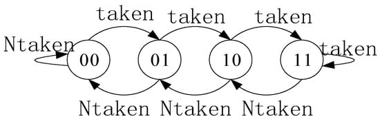
Figure 2.
State Transition of Saturated Counter.
In the Gselect branch predictor architecture, the high-order bits of the program counter are simply concatenated with the low-order bits of the branch history register, then truncated to K bits to index the PHT. This approach fails to fully utilize the low-order bits of the program counter, causing the branch predictor to assign the same PHT index value to instruction sequences with similar high-address patterns. This triggers address mapping conflicts in the prediction table—known as branch aliasing—ultimately degrading Gselect’s branch prediction accuracy [31]. To resolve this, this paper proposes a branch prediction architecture based on TXOR-Gselect (Two-level branch predictor). This structure effectively mitigates the inherent branch aliasing issue in the Gselect architecture, thereby enhancing branch prediction accuracy. Its specific structure is illustrated in Figure 3.
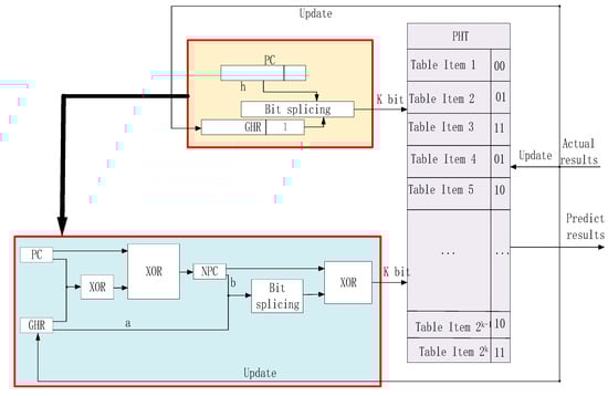
Figure 3.
TXOR-Gselect Predictor.
As shown in Table 2, in the traditional Gselect branch predictor, although the program counter values (PC) and global history register values (GHR) for both example branch instructions are distinct (PC1 = 1010001111001111, GHR1 = 0011110010101010; PC2 = 1010001100000001, GHR2 = 1010111110101010), they are mapped to the same PHT index (1010001110101010) due to limitations in the index generation mechanism. This results in branch aliasing issues, significantly degrading prediction accuracy. This paper proposes the TXOR-Gselect architecture, which reconstructs index generation logic through multi-level XOR and bit concatenation operations. Taking Example 1 as an illustration, PC is 1010001111001111 and GHR is 0011110010101010. First, perform bitwise XOR between PC and GHR to obtain the intermediate result 1001111101100101. Then, XOR this result with PC again to yield the NPC value 0011110010100100. Next, extract the high b bits of NPC (in this case, b = 00111100) and the low a bits of GHR (in this case, a = 10101010), concatenating them into a 16-bit value: 0011110010101010. Finally, perform an XOR operation between NPC and this concatenated value to obtain the PHT index value 0000000000001110. In Example 2, since PC and GHR differ, the entirely new index value generated through the same process is 0000000000000000. This effectively prevents index overlap at the hardware level.
Table 2.
Introduction to Indexes generated by Gselect and TXOR-Gselect.
This paper evaluates the performance of the improved branch predictor using six test sets. Multiple experiments demonstrate that under the configuration of GHR length set to 12 and PHT capacity fixed at 2048 entries, the accuracy of the three branch prediction strategies—Static Branch Predictor (SBP), Gselect, and TXOR-Gselect—is further compared and analyzed. Figure 4 presents the accuracy comparison results of these three branch predictors across the six standard test sets.
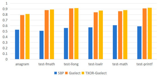
Figure 4.
Branch Prediction Accuracy Comparison.
As shown in Figure 4, the TXOR-Gselect branch predictor outperforms the original Gselect predictor. Under a GHR length of 12, its average prediction accuracy reached 88.02%, representing a 1.47 percentage point improvement over the Gselect predictor’s 86.55%, demonstrating superior branch prediction capability. The branch predictor is integrated into the instruction fetch stage, with a fixed one-cycle latency. The pattern history table and branch target buffer capacities are set to 1024 entries and 512 entries, respectively, aligning with typical hardware resource constraints in embedded scenarios. The cache size is 64 KB with a 5-cycle hit latency. In the test program, the baseline Gselect predictor achieved an average IPC of 0.75, while integrating the TXOR predictor increased the average IPC to 0.762. Although this absolute performance gain may appear modest, it must be considered against the backdrop of Gselect’s already high baseline performance. Crucially, implementing TXOR-Gselect requires only a minimal addition of XOR operations to Gselect’s indexing logic, resulting in hardware overhead that is virtually negligible compared to Gselect. This performance improvement achieved at near-zero cost demonstrates the practicality and efficiency of our approach.
- (2)
- Jump Address Prediction
The Target Address Buffer Table is a storage unit composed of multiple table entries, essentially functioning as a cache structure. To balance prediction accuracy and hardware overhead, the table size is set to 512 entries. Each entry comprises three primary components: the Valid bit, the Branch Instruction Address, and the Target Address. The BTB prediction process, illustrated in Figure 5, uses the branch instruction to index the table entries. It compares the branch instruction address with the stored branch instruction addresses in the table. If a hit occurs and the corresponding entry’s Valid bit is set to true, the jump target address is extracted from that entry as the predicted address. This address is then passed to the PC fetch module to serve as the fetch address for the next instruction. This mechanism effectively reduces pipeline stalls caused by branch instructions by rapidly providing the jump target address, thereby enhancing the processor’s fetch efficiency.
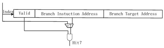
Figure 5.
BTB Prediction Mechanism.
- (3)
- Branch Prediction Correction Module (Set Module)
In branch prediction technology, predictions inevitably fall into two categories: correct and incorrect. When a prediction is correct, the pipeline executes smoothly. When a prediction is incorrect, the instructions already executed on the erroneous path must be promptly corrected, and the execution must switch to the correct path. If this process is mishandled, it can result in severe performance penalties. The branch prediction correction module assumes this critical verification and error-correction responsibility. This module compares the predicted branch instruction outcome with the actual result, determining whether and how to correct errors based on this comparison. The following sections detail the module’s design specifics, operational workflow, and its vital role within the processor.
When the PC module generates an instruction address, that address may point to a control flow transfer instruction. In this case, the address serves as an index to access the branch prediction table and retrieve the predicted target address. During pipeline execution, only when the instruction enters the execution stage can actual computation confirm whether a jump actually occurred. However, before the jump determination is complete, the instruction corresponding to the predicted target address may have already entered the decoding stage. Therefore, during the execution phase, the processor compares the actual computed target address with the predicted address: if they match, the branch prediction is correct and execution continues; if they differ, the prediction is incorrect and an address correction is required. When a prediction error occurs, all instructions fetched during decoding and fetching based on the incorrect prediction become invalid. The relevant pipeline stages must be flushed, and the PC value updated to the actual target address.
Specifically, if the branch predictor anticipates a jump and feeds the predicted address into the PC module, but the execution phase determines that the instruction should not actually jump (i.e., it executes sequentially, with the next instruction address being the current address plus 4), the computed sequential address (PC + 4) must be rewritten into the PC module. This ensures the processor continues executing the correct instruction stream. This error correction mechanism dynamically detects and corrects prediction deviations, effectively reducing the performance overhead caused by branch prediction failures while enhancing pipeline execution efficiency and processor fault tolerance.
The core design of this module is a combinational logic circuit, whose decision logic is based on four possible combinations of the predicted branch signal (predict_jump_flag_i) and the actual branch signal (act_jump_flag_i). First, it determines whether the predicted address equals the actual address. Subsequently, it combines the two jump flags via a case statement to ultimately generate the jump control signal. addr_equal determines whether the predicted jump address matches the actual jump address. It remains high (1) if they match and goes low (0) if they differ. The signals involved in this module are shown in Table 3. Its core decision logic is represented as follows: When both prediction and actual jumps occur and addr_equal is high (1), the module determines that the prediction is correct. It does not pull the correction signal (jump_flag_o) high and requires no jump address correction (jump_addr_o). If both indicate a jump and addr_equal is 0, it is deemed a prediction error; the correction signal is pulled high, and the jump address is corrected. When a predicted jump occurs but the actual jump does not, it constitutes a prediction error; the correction signal is pulled high, and the jump address is corrected to PC + 4 to guide the pipeline back to the correct path.
Table 3.
Introduction to Signals of Figure 6.
The key code for this section is shown in Figure 6.
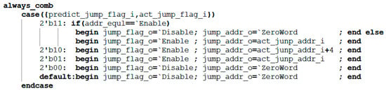
Figure 6.
Key Code for the Correction Module.
3.3.2. Division Optimization Based on Data Correlation
- (1)
- Divider Module
In the SHriscv architecture, the divider employs the trial division method. The division instruction is a long-cycle operation, requiring 33 clock cycles for the Div module to complete a single division. Traditional processors must halt for 33 clock cycles during division, leading to pipeline stalls. This research proposes an optimization method based on a data-correlation detection and forwarding mechanism. Under this mechanism, the divider can operate continuously as an independent module while the processor executes other instructions in parallel, thereby optimizing the operational speed of the SHriscv processor.
Before introducing the bypass forwarding mechanism discussed in this paper, consider the following RISC-V processor assembly code:
| 0012: | addi | x1, x2, 12 |
| 0016: | addi | x3, x1, 12 |
| 0020: | div | x7, x8, x9 |
| 0024: | add | x4, x3, x1 |
From the above assembly code, it can be seen that the execution result of instruction 0012 affects the execution result of instruction 0016. The execution results of both 0016 and 0012 jointly influence the execution result of instruction 0024. However, the final calculated value of the division instruction 0020 does not affect the execution status of 0024. This study introduces a detect-and-forward mechanism into a five-stage pipeline. Specifically, if a division instruction is detected and subsequent instructions require the result of this division operation, the pipeline pauses until the division completes. The division result is then replaced in the corresponding destination register. If the division result is not required, the processor continues its instruction fetch and execution flow.
As illustrated in the example above, the division instruction executed at address 0020 does not affect the addition instruction at address 0024. In this case, the processor need not pause to wait for the division instruction to complete; it may proceed to fetch and execute the addition instruction. With the addition of the data dependency module, the divider’s operation does not interfere with the PC module’s continued instruction fetching when no data conflicts occur, thereby enhancing the processor’s instruction fetch speed.
During the execution phase of each instruction, the system performs dependency checks (signals involving data dependencies within the module are shown in Table 4): It compares the RS1 address of the current instruction (reg_raddr1_i in Figure 7) with the target register address of the execution stage (ex_reg_waddr_i in Figure 7), the division register address (div_waddr_reg in Figure 7), the memory access stage register address (mem_reg_waddr_i in Figure 7), and the write-back stage register address (wb_reg_waddr_i in Figure 7). If the RS1 address matches any of the above addresses, the system prioritizes forwarding the precomputed data to the required stage. The detailed workflow is as follows: First, if RS1 is the zero register (x0), the zero value is returned directly. Second, perform the highest-priority execution and division unit checks: if a division operation is in progress, halt the front end and clear the decode stage; if the division completes within the current cycle, pass its result to RS1. Third, if an execution-level instruction requires writing to the same register, further checks occur: for load instructions, similarly, halt the front end and clear the decode stage; if it is a non-load instruction, the execution stage result is directly propagated. Subsequently, the module sequentially checks the memory access and write-back stages. If a valid write register operation exists, the corresponding data is propagated. If none of the above propagation conditions are met, the original data is ultimately read from the register file as the operand value.
Table 4.
Introduction to Signals of Figure 7.
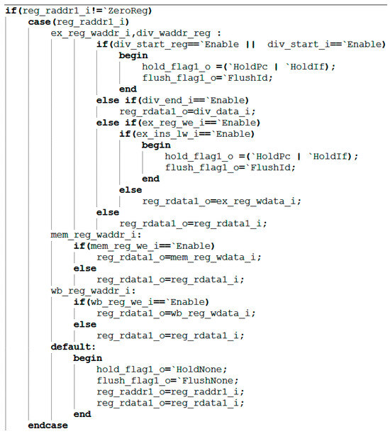
Figure 7.
Execution code of the target register rs1.
The execution code for register rs1 is shown in Figure 7. The processing method for other registers is the same.
3.3.3. Storage Structure Optimization
This paper implements a cache module based on a set-associative architecture, supporting multi-way set-associative mapping and a pseudo-LRU (Least Recently Used) replacement strategy. The cache employs a write-back consistency policy and performs replacement operations during misses. Its core structure includes a data storage unit, a tag storage unit, a valid bit, and a dirty bit, all organized by set and way. Read/write requests access data directly upon hits. For misses, the LRU policy selects a replacement line; if that line is dirty, it is first written back to memory before swapping in new data. A state machine controls three states—IDLE, SWAP_OUT, and SWAP_IN—ensuring data consistency and transaction atomicity. This design achieves efficient addressing through address decomposition (Tag, Set, Line, Word), supports concurrent read/write detection and pipelined memory access, delivering excellent timing performance and resource utilization.
Figure 8 illustrates the storage architecture of this paper, employing a custom bus to connect the processor and peripheral devices. A UART module is implemented to facilitate the output of program execution results. In the cache design, its capacity is set to 32 kB, with each way containing 64 cache lines. A four-way set-associative mapping strategy is adopted to balance cache hit rate and hardware overhead. The four-way set-associative design effectively reduces cache conflicts and enhances data access efficiency. The replacement algorithm abandons the traditional Least Recently Used (LRU) strategy in favor of a pseudo-LRU algorithm to conserve resources. This design also supports cache enable/disable functionality. When disabled, the processor core can directly access memory via the custom bus, requiring 19 clock cycles for memory access. When enabled, memory access requires only one clock cycle, significantly reducing processor memory access latency.
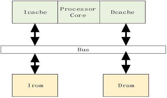
Figure 8.
Processor Storage Architecture Design Diagram.
When the instruction cache (Icache) is enabled, the processor preloads data from Irom into the Icache and executes the program starting from the specified starting address. Similarly, the access mechanism for the Dcache (Data Cache) aligns with that of the Icache. Furthermore, this paper incorporates write strategy optimization into the cache design, employing write-back and write-allocate strategies to reduce frequent writes to main memory, lower power consumption, and enhance system performance. By accessing data through the cache, communication overhead between the processor core and main memory is minimized, further accelerating data access speeds.
4. Processor Verification and Analysis
4.1. Hardware and Software Platform
This paper implements the SHriscv processor architecture using the Verilog hardware description language and evaluates the performance of the processor core through the CoreMark benchmark suite. During experimentation, the operating system utilized the IC_EDA_Lite virtual machine from Core Kingdom (which includes tools like Questasim, VCS, Verdi, and a 32-bit RISC-V toolchain). Vivado HLS 2018.3 EDA development tools were employed to conduct functional verification and performance testing on both pre-optimized and optimized processor platforms. The experimental platform utilized Xilinx ATRIX-7 series FPGAs (model: XC7A100T). After applying multiple optimization techniques, all processors successfully operated on this hardware platform. For the software toolchain, the official RISC-V Eclipse compiler generated executable files, which were then downloaded to the FPGA via the Opcode tool for functional verification and performance testing.
4.2. Functional Testing
Testing the processor core primarily involves several steps: (1) Load the test file; (2) Use the serial port emulator to send the file to the ROM (Read-Only Memory); (3) Use the serial port emulator to send the boot command to the processor, which then completes the program file transfer; (4) Begin executing the test program until the PASS statement; (5) Iterate through all test files.
The RISC-V International Foundation provides a set of instruction set test programs to verify whether RISC-V processor implementations comply with the specification. Its primary purpose is to validate whether the instructions supported by the designed processor have been successfully implemented. Testing the processor core using these instruction set test programs revealed that the optimized processor performed exceptionally well in the instruction set tests. Figure 9 reveals a performance bottleneck in the prototype processor during division operations: regardless of data dependency, the processor must halt the pipeline until the division completes before fetching the next instruction. After implementing division optimization based on data dependency, as shown in Figure 10, the improved processor can continue fetching instructions while executing division operations, significantly enhancing instruction fetch speed. Under ideal conditions, division calculations no longer require pipeline stalls, saving 33 clock cycles (division operations take 33 clock cycles). The reduction in division computation time amounts to 100%. Regarding branch prediction, Figure 11 demonstrates that the proposed dynamic branch predictor efficiently forecasts jump addresses. Figure 12 further validates that when prediction results diverge from actual jump paths, the prediction error correction module promptly restores processor state, ensuring correct instruction stream execution. Additionally, experimental data in Figure 13 indicates that the SHriscv processor significantly enhances memory access rates by integrating cache modules and peripheral device interfaces.
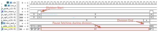
Figure 9.
The preprocessor cannot continue fetching instructions during division before optimization.
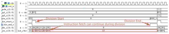
Figure 10.
The optimized post-processor can continue fetching instructions during division.
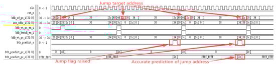
Figure 11.
The dynamic branch predictor can predict the jump address.
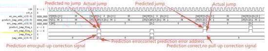
Figure 12.
Correction of the Correction Signal When the Dynamic Branch Predictor Makes a Prediction Error.
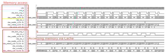
Figure 13.
The processor accesses memory through the cache.
4.3. Performance Testing
This paper evaluates processor performance using the CoreMark benchmark suite. CoreMark is a comprehensive embedded processor performance evaluation test suite that has become an industry-recognized standard for CPU (Central Processing Unit) performance assessment [32]. To conduct the performance testing, the CoreMark test program was ported to Shriscv, and a UART module was developed to support test result output. The experimental platform utilizes the Xilinx XC7A100T development board operating at a 50 MHz clock frequency. During testing, data was transmitted to the PC via a serial communication interface, with final results displayed in a serial debugging tool. Detailed CoreMark performance results for the experiment are shown in Figure 14. The test results demonstrate that this processor architecture exhibits excellent performance characteristics in embedded application scenarios.
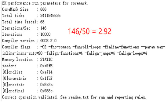
Figure 14.
CoreMark Benchmark Test Results.
Figure 14 presents the serial port output data from the processor executing the CoreMark benchmark after comprehensive optimization. Experimental results indicate that when all performance optimization strategies are enabled, the CoreMark performance evaluation score for this processor architecture reaches 2.92 CoreMark/MHz. This quantitative outcome fully validates the effectiveness of the proposed optimization strategies in enhancing processor performance, providing a reliable performance metric for evaluating the computational capability of embedded processors.
4.4. Analysis of Experimental Results
Table 5 details the CoreMark performance scores for this processor architecture with different optimizations enabled. Without any optimizations, the processor achieves a performance score of 2.4 CoreMark/MHz. Enabling the Data Cache (Dcache) optimization boosts the score to 2.6 CoreMark/MHz. This improvement primarily stems from enhanced data access efficiency. However, the high miss rate of DCache during the initial phase limits the extent of performance gains. Further enabling the instruction cache (Icache) significantly boosts the performance score to 2.81 CoreMark/MHz. This is because instructions can be fetched directly from the ICache, substantially reducing the processor’s time overhead for accessing external memory. Introducing the dynamic branch prediction mechanism achieves a performance score of 2.92 CoreMark/MHz, confirming that this mechanism effectively reduces the time overhead caused by pipeline flushes due to branch instruction jumps. It is noteworthy that although division optimization improved computational speed, division instructions accounted for less than 0.5% of the CoreMark test suite. Consequently, this optimization did not significantly impact the overall performance score. This series of experimental data fully validates the effectiveness of each optimization strategy and its contribution to processor performance.
Table 5.
Detailed CoreMark Benchmark Results of the Processor.
Using Synopsys’ Design Compiler tool and the SIMC 110 nm process, the processor designed in this paper underwent logic synthesis. The CoreMark benchmark test results and comparisons with other processors are listed in Table 6. Compared to the ARM Cortex-M0 and E203, the processor designed in this paper exhibits higher power consumption and area but achieves significant performance improvements. Compared to the ARM Cortex-M3, its performance is lower, but its area is reduced by 31.67% and its power consumption is decreased by 0.32 mW. Experimental data analysis indicates that this processor architecture significantly outperforms most processors in key performance metrics.
Table 6.
Power Consumption Performance Comparison of Different Processors.
5. Conclusions and Future Work
This paper focuses on sequential pipeline processors based on the RISC-V instruction set architecture and proposes a series of optimization schemes. Key optimizations include: (1) proposing a TXOR-Gselect branch prediction algorithm that effectively mitigates branch aliasing through a three-stage XOR indexing mechanism; (2) designing an optimizer for dividers that supports data correlation detection and forwarding, significantly reducing pipeline stalls caused by division operations; (3) Implementing a four-way set-associative cache structure with a pseudo-LRU replacement strategy to improve memory access latency. The optimized processor underwent comprehensive board-level functional verification on the Xilinx FPGA platform. Performance evaluation using the CoreMark benchmark revealed a significant improvement in score from the initial 2.4 CoreMark/MHz to 2.92 CoreMark/MHz, outperforming most open-source processor implementations of comparable scale.
Experimental results indicate that this processor architecture still holds potential for further optimization: On one hand, leveraging the characteristics of the RISC-V instruction set enables in-depth exploration of areas such as the Memory Management Unit (MMU) and multithreading support. Enabling the MMU for memory address translation and access control introduces minimal clock cycle overhead, theoretically exerting a negligible impact on single memory access latency. However, this small trade-off for security and process isolation is both necessary and worthwhile. Implementing multithreading significantly boosts overall system throughput, though it introduces resource trade-offs: duplicating register sets, adding hardware overhead for thread scheduling logic, and potential contention issues from shared cache resources. This research methodology can be extended to multi-core processor scenarios to investigate the impact of task scheduling and resource sharing on real-time performance. On the other hand, introducing pipelined division operations holds promise for further enhancing computational efficiency within the division module, as pipelined division enables initiating new division calculations per clock cycle, thereby achieving superior overall performance.
Author Contributions
Investigation, Z.J. (Zhiwei Jin) and P.W.; Resources, T.H.; Writing—original draft, T.H.; Writing—review & editing, T.H. and Z.J. (Zhiyi Jie); Supervision, Z.J. (Zhiwei Jin) and P.W. All authors have read and agreed to the published version of the manuscript.
Funding
This research received no external funding.
Institutional Review Board Statement
Not applicable.
Informed Consent Statement
Not applicable.
Data Availability Statement
The original contributions presented in the study are included in the article, further inquiries can be directed to the corresponding author.
Conflicts of Interest
The authors declare no conflicts of interest.
References
- Hennessy, J.L.; Patterson, D.A. Computer Architecture: A Quantitative Approach, 6th ed.; China Machine Press: Beijing, China, 2017; pp. 45–50. [Google Scholar]
- Waterman, A.; Asanović, K. RISC-V Instruction Set Manual, Volume 1: User-Level ISA; RISC-V Foundation: Zürich, Switzerland, 2019; pp. 12–18. [Google Scholar]
- Lai, J.; Wei, H.; Sun, K.; Wang, Y. A Neural Network Acceleration System Based on PYNQ. Electron. Des. Eng. 2024, 32, 16–21. [Google Scholar]
- Di, L.; Rui, C.; Ying, L. Research on Application Porting Process Platform from X86 Architecture to ARM Architecture. Electron. Des. Eng. 2022, 30, 176–179+184. [Google Scholar]
- Asanović, K.; Avizienis, R.; Bachrach, J.; Beamer, S.; Biancolin, D.; Celio, C.; Cook, H.; Dabbelt, D.; Hauser, J.; Izraelevitz, A.; et al. Rocket Chip Generator; Berkeley Technical Report; University of California: Berkeley, CA, USA, 2016. [Google Scholar]
- Celio, C.; Patterson, D.A.; Asanović, K. BOOM Processor: A Multicore Research Platform; Berkeley Technical Report; University of California: Berkeley, CA, USA, 2015. [Google Scholar]
- Taheri, F.; Bayat-Sarmadi, S.; Hadayeghparast, S. RISC-HD: Lightweight RISC-V processor for efficient hyperdimensional computing inference. IEEE Internet Things J. 2022, 9, 24030–24037. [Google Scholar] [CrossRef]
- Li, T.; Cui, E.; Wu, Y.; Wei, Q.; Gao, Y. TeleVM: A lightweight virtual machine for RISC-V architecture. IEEE Comput. Archit. Lett. 2024, 23, 121–124. [Google Scholar] [CrossRef]
- Sun, Y. RISC-V Advances Rapidly, Promising Future Prospects. Commun. World 2024, 17, 5. [Google Scholar]
- Liu, X.; Lin, H.; Liu, P. Overview of the RISC-V Instruction Set Architecture and Its Applications. China Integr. Circuits 2025, 34, 16–20+49. [Google Scholar]
- Zhang, X. Academician Ni Guangnan of the Chinese Academy of Engineering: Contributing Chinese Wisdom to the Prosperity of the RISC-V Ecosystem. China Electronics News, 29 November 2024; pp. 2–9. [Google Scholar]
- Patterson, D.; Waterman, A. The Art of RISC-V Open Architecture Design; Electronics Industry Press: Beijing, China, 2024; pp. 230–245. [Google Scholar]
- Deng, Y. Leading the Chip Customization Revolution—SiFive 2018 Shanghai Technical Seminar Successfully Held. China Integr. Circuits 2018, 27, 17–18+26. [Google Scholar]
- Silei, L.; Zheng, X. Research on Open-source SoC Freedom E310 Debugging Method. Microcontroll. Embed. Syst. 2017, 17, 59–62. [Google Scholar]
- Xu, L. “One Life, One Chip” Initiative: Tackling the Bottleneck in Chip Talent Development. Guangming Daily, 28 November 2021; p. 6. [Google Scholar]
- Wu, Y.; Qiao, J.; Lei, G.; Su, Y. Research and Design of RISC-V Processors for Edge Nodes. Electron. Devices 2024, 47, 1451–1456. [Google Scholar]
- Lin, O. Design of a RISC-V Processor for Power Supply Controllers. Master’s Thesis, University of Chinese Academy of Sciences (Institute of Modern Physics, Chinese Academy of Sciences), Beijing, China, 2024; pp. 1–5. [Google Scholar]
- Zhang, X.; Liang, Q.; Li, T. Design and Implementation of an RV32I Control Unit. Microelectron. Comput. 2018, 35, 74–78+82. [Google Scholar]
- Li, Y.; Jiao, J.; Liu, Y.; Hao, Z. Research and Design of an Embedded RISC-V Out-of-Order Execution Processor. Comput. Eng. 2021, 47, 261–267+284. [Google Scholar]
- Jie, G. Research on Embedded RISC-V Microprocessor Architecture. Master’s Thesis, Central South University, Changsha, China, 2023; pp. 1–6. [Google Scholar]
- Li, D.; Cao, K.; Qu, M.; Wang, F. Hardware/Software Co-Emulation Verification of a Five-Stage Pipeline RISC-V Processor. J. Jilin Univ. (Inf. Sci. Ed.) 2017, 35, 612–616. [Google Scholar] [CrossRef]
- Li, Q. Design and Analysis of a RISC-V Microcontroller for IoT End Devices. Microcontroll. Embed. Syst. Appl. 2018, 18, 64–66. [Google Scholar]
- Patterson, D.A.; Hennessy, J.L. Computer Organization and Design, RISC-V Edition: The Hardware/Software Interface; Morgan Kaufmann Publishers Inc.: San Francisco, CA, USA, 2017. [Google Scholar]
- Mith, A. Cache Memory. ACM Comput. Surv. 2018, 50, 1–35. [Google Scholar]
- Yeh, T.-Y.; Patt, Y.N. Two-Level Adaptive Training Branch Prediction. J. Comput. Archit. 2019, 26, 45–52. [Google Scholar]
- Li, R.; Chen, J.; Liu, W. Architecture Optimization Based on the Xinlai Hummingbird E203 Processor. Electron. Des. Eng. 2025, 33, 6–11+16. [Google Scholar]
- Zhou, X.; Cai, G.; Huang, Z. Design and Implementation of RISC-V Extended Instruction Set Supporting FPGA Dynamic Reconfiguration. Comput. Eng. 2025, 51, 229–238. [Google Scholar]
- Xie, H.; Xiao, Q.; Zhu, Z.; Liu, Y.; Liu, Y. Development and Apssplication of Vector Instruction Set and Communication Extension Instruction Set Based on RISC-V Architecture in 5G Redcap Baseband Processor. China Informatiz. 2024, 1, 89–90. [Google Scholar]
- Simin, J. Research on RISC-V Processor Core Design Optimization and Extended Instruction Set Implementation. Master’s Thesis, Shandong University, Jinan, China, 2023; pp. 19–26. [Google Scholar]
- Wen, G. Analysis and Optimization of the Branch Prediction Unit in SweRV EH1. Master’s Thesis, Xiamen University, Xiamen, China, 2022; pp. 10–15. [Google Scholar]
- Kim, H.K.; Kim, H.S.; Eun, C.M.; Cho, H.H.; Jeong, O.H. A high-performance branch predictor design considering memory capacity limitations. In Proceedings of the 2017 International Conference on Circuits, System and Simulation (ICCSS), London, UK, 14–17 July 2017; IEEE: Piscataway, NJ, USA, 2017; pp. 49–53. [Google Scholar]
- Zhang, Y. Design of a High-Performance Embedded Processor Supporting the RV64IMCB Instruction Set. Master’s Thesis, Xiamen University, Xiamen, China, 2022; pp. 80–90. [Google Scholar]
- Wei, Y.; Yang, Z.; Tie, J.; Shi, W.; Zhou, L.; Wang, Y.; Wang, L.; Wu, X. A Multistage Dynamic Branch Predictor Based on Hummingbird E203. Comput. Eng. Sci. 2024, 46, 785–793. [Google Scholar]
- Martin, T. The Designer’s Guide to the Cortex-M Processor Family; Newnes: Boston, MA, USA, 2022. [Google Scholar]


Disclaimer/Publisher’s Note: The statements, opinions and data contained in all publications are solely those of the individual author(s) and contributor(s) and not of MDPI and/or the editor(s). MDPI and/or the editor(s) disclaim responsibility for any injury to people or property resulting from any ideas, methods, instructions or products referred to in the content. |
© 2025 by the authors. Licensee MDPI, Basel, Switzerland. This article is an open access article distributed under the terms and conditions of the Creative Commons Attribution (CC BY) license (https://creativecommons.org/licenses/by/4.0/).