Abstract
With continued CMOS scaling, transistor miniaturization has significantly raised SRAM integration density while lowering the critical charge (Qc), increasing cell vulnerability to spaceborne high-energy particles. Single-event upset (SEU) and especially single-event multiple node upsets (SEMNU) due to charge sharing present major reliability challenges. To overcome these issues, this study introduces a radiation-hardened 20T SRAM cell with read/write optimization (RWO-20T) designed for space applications. Benchmarking against hardened cells RH14T, RHSCC16T, S8P8N16T, and CC18T reveals that RWO-20T delivers superior read static noise margin (RSNM), increased word-line write trip voltage (WWTV), and faster read and write access times. Although the higher transistor count incurs some area overhead and slightly lowers the hold static noise margin (HSNM), RWO-20T achieves improved recovery rates for dual-node upsets (DNU) and triple-node upsets (TNU) under SEMNU conditions. The circuits were simulated in a 90 nm CMOS process and operated at 1 V.
1. Introduction
In the space industry, static random-access memory (SRAM) serves as cache for high-performance processors thanks to its rapid access and real-time processing capabilities. Particularly, organizations such as NASA and ESA enforce strict requirements for space-grade components, including resilience to single-event effects (SEE), total ionizing dose (TID) tolerance, low power consumption, and system reliability. Radiation-hardened SRAM, designed to withstand the harsh radiation environment of space, serves as a critical component. Advances in CMOS scaling have dramatically increased SRAM density but shrinking transistor dimensions also reduce node capacitance [1]. Consequently, the critical charge (Qc), the minimum collected charge needed to invert a stored bit, diminishes [2], making SRAM more prone to SEE induced by high-energy particles in space [3]. This trend highlights the need for next-generation, space-qualified SRAM with enhanced resilience to soft errors.
High-energy particles in the universe can strike a transistor and ionize semiconductor atoms, creating electron–hole pairs that are carried to sensitive circuit nodes by drift or diffusion [4]. If enough charge is deposited, a single event transient (SET) may form; should this transient’s charge exceed the critical charge Qc, a single-event upset (SEU) can flip the stored value at an SRAM node [2]. Furthermore, as device geometries shrink, the reduced separation between nodes increases charge-sharing after a single particle hit, potentially causing single-event multiple-node upsets (SEMNU) in which several bits invert simultaneously [5]. The continued scaling of CMOS technology, which lowers both Qc and inter-node distances, thus heightens the frequency and impact of soft errors, posing a growing reliability concern for SRAM in radiation-exposed space systems [6].
Various solutions have been developed to address reliability concerns in space memory, such as triple modular redundancy (TMR) and error correction codes (ECC), which help mitigate the effects of SEU and SEMNU [7]. Nevertheless, these techniques often lead to substantial increases in latency, power consumption, and silicon footprint, rendering them ill-suited for fast, real-time applications in space environments [8]. Consequently, radiation-hardened-by-design (RHBD) strategies have taken on a central role in the development of space-grade SRAM, directly reinforcing the cell’s robustness against both SEU and the growing challenge of SEMNU while maintaining efficiency in area and operational performance [9].
The RH-14T [10] cell employs an asymmetric configuration with five internal nodes, which provides robust protection against double-node upset (DNU) but lacks full SEU immunity. The RHSCC-16T [11] design increases complexity to six internal nodes, offering strong resistance to SEMNU, yet the higher count of sensitive nodes raises the potential for charge-sharing-induced SEMNU. Both the S8P8N-16T [12] and the CC-18T [13] architectures prioritize low power consumption while achieving elevated word-line write trip voltages (WWTV) and faster write access times (WAT). Their primary compromise is between hold stability and upset tolerance: the S8P8N attains a higher Qc at the expense of a lower hold static noise margin (HSNM), whereas the CC-18T secures a better HSNM but with a reduced Qc. Despite these improvements, both designs exhibit relatively modest read static noise margins (RSNM). Although highly SEU-robust SRAM architectures like DICE-10T and DICE-12T [14] exist, this study focuses on comparing SRAM designs developed based on the fundamental 6T structure.
Conventional RHBD cells invariably involve trade-offs, such as larger cell area, slower access times, and only partial recovery under certain upset scenarios, and, in space applications where reliability is critical, achieving an optimal balance of read/write stability, fast access time, and high SEU/SEMNU recovery is indispensable [7].
The purpose of this paper is to design an SRAM device that provides full SEU immunity, high SEMNU tolerance, and optimized read and write performance with minimal capability loss or area increase due to trade-offs. Proposed RWO-20T SRAM is designed with 20 transistors and 6 internal nodes in a symmetric architecture to address the low restoration capability of existing radiation-hardened SRAMs against SEMNU and achieves full restoration following any SEU. Relative to prior radiation-hardened designs, RWO-20T delivers superior RSNM, WWTV, read access time (RAT), and WAT. Although its higher transistor count incurs a modest increase in cell area and a slight reduction in HSNM, RWO-20T exhibits markedly improved resilience against DNU and triple-node upset (TNU) within SEMNU scenarios. This combination of robust multi-node recovery and high-performance read/write characteristics makes RWO-20T exceptionally well suited for reliable memory operations in harsh space environments.
2. Proposed Cell
2.1. Operation of Proposed Cell
Figure 1 presents the RWO-20T cell’s circuit schematic, Figure 2 shows its corresponding layout, and Figure 3 illustrates its operational waveforms. The RWO-20T employs a total of twenty transistors to form six internal nodes: two storage nodes (Q and QB) and four auxiliary nodes (S1, S0, S3, S2). Transistors N4 and N5 are enlarged to 2.5 × minimum width to boost read performance, while all other devices are set to the author’s chosen minimum size. Access transistors N8, N9, N10, and N11 are gated by the word line (WL), such that asserting WL to VDD electrically connects their respective nodes to the bit lines (BL or BLB). Nodes S3 and S2 derive their logic values from the current states of Q, QB, S1, and S0; by contrast, S1 and S0 only toggle when Q, QB, S3, and S2 all switch in unison. This multi-tiered feedback arrangement grants the cell full immunity to SEU, enables robust restoration after DNU, and provides tolerance to TNU. Throughout all analyses, the cell is assumed to begin in the logic ‘1’ configuration, where Q = S1 = S3 = ‘1’ and QB = S0 = S2 = ‘0’.
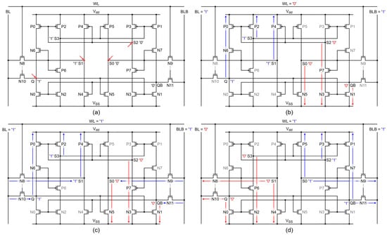
Figure 1.
(a) Schematic with sensitive nodes. (b) Hold mode. (c) Read mode. (d) Write mode.
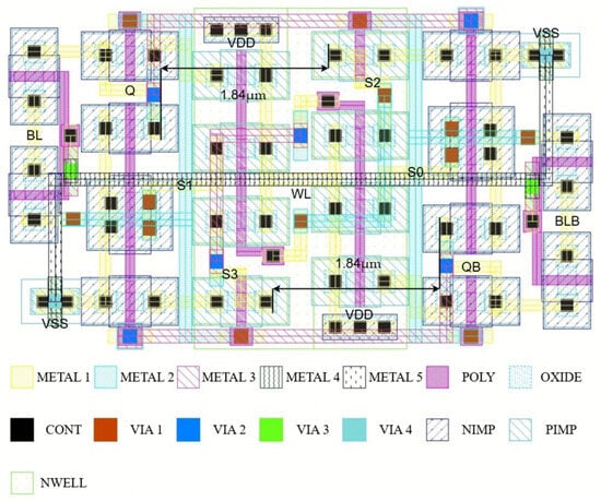
Figure 2.
Layout of the RWO-20T cell.
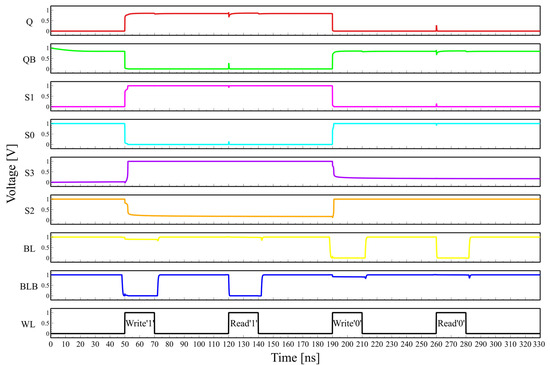
Figure 3.
Waveform demonstrating the basic operation of the proposed cell.
2.1.1. Hold Operation
During the hold operation, the WL is set to VSS, which turns off all access transistors (N8, N9, N10, and N11). This action disconnects the cell from both BL and BLB, internally isolating it and preventing any read or write access. To support rapid readout and avoid malfunction, BL and BLB are both pre-charged to VDD [15]. As previously indicated, when ‘1’ is stored in the cell, Q = ‘1’ means that N1, N3, and N5 are turned on, while QB = ‘0’ results in N0, N2, and N4 being turned off. For S1 = ‘1’, N6 is turned on and P6 is turned off; with S0 = ‘0’, N7 is turned off and P7 is turned on. In the case that S3 is set to ‘1’, P1, P3, and P5 are turned off, and when S2 is set to ‘0’, P0, P2, and P4 are turned on. The ‘1’ logic state at the Q, S1, and S3 nodes is sustained via the pull-up paths Q-N6-P0-VDD, S1-P4-VDD, and S3-P2-VDD, respectively. Meanwhile, nodes QB, S0, and S2 keep the ‘0’ state through the pull-down paths QB-N1-VSS, S0-N5-VSS, and S2-P7-N3-VSS. Any transistors not engaged in these pull-up or pull-down paths stay turned off, ensuring that the state of every node is reliably maintained.
2.1.2. Read Operation
In the read operation, WL is driven to VDD, activating all access transistors (N8, N9, N10, and N11). As a result, Q and S1 are connected to BL via N8 and N10, respectively, while QB and S0 are linked to BLB through N9 and N11. Because the pull-up paths keep Q and S1 at ‘1’, BL remains at its pre-charged level. Meanwhile, QB and S0 holding ‘0’ pull BLB down through the paths BLB–N9–S0–N5–VSS and BLB–N11–QB–N1–VSS. Once the voltage difference between BL and BLB reaches approximately 50 mV, the sense amplifier detects this differential and reads out the stored value.
2.1.3. Write Operation
For the write operation, the WL is also set to VDD, turning on all access transistors. When writing a ‘0’ over a previously stored ‘1’, BL is pre-discharged to VSS and BLB is pre-charged to VDD. Using N8 and N10, Q and S1 are pulled down to ‘0’ via BL, while via N9 and N11, QB and S0 are set to ‘1’ using BLB. As Q is pulled to ‘0’, N1, N3, and N5 are turned off; simultaneously, with QB set to ‘1’, N0, N2, and N4 are turned on. As S1 is pulled down to ‘0’, N6 is turned off and P6 is turned on. Likewise, when S0 is set to ‘1’, N7 is turned on while P7 is turned off. With N2 and P6 both turned on, S3 is pulled low; when P1, P3, and P5 are all turned on, P3 turns on as well to pull S2 up to ‘1’. Ultimately, all node values change to Q = S1 = S3 = ‘0’ and QB = S0 = S2 = ‘1’, which finalizes the write process.
2.2. SEU Recovery Analysis
When a high-energy particle strikes the drain of an idle transistor, it induces a transient pulse whose polarity depends on the device type [7]. In PMOS devices, the pulse is positive, potentially driving a stored ‘0’ up to ‘1’ (or reinforcing a ‘1’), whereas in NMOS devices, the pulse is negative, possibly pulling a stored ‘1’ down to ‘0’ (or reinforcing a ‘0’). Only those transitions that actually invert the stored bit—‘0’→‘1’ or ‘1’→‘0’—are of concern for SEU analysis; pulses that leave the bit unchanged (‘0’→‘0’ or ‘1’→‘1’) do not affect data integrity [16]. Accordingly, nodes are classified based on their susceptibility: if an SEU cannot alter its state given its stored value and surrounding transistor network, it is “non-sensitive,” while nodes that can flip are “sensitive.” For instance, in the RWO-20T cell initialized to ‘1’, the QB node, composed solely of NMOS transistors and holding ‘0’, would only ever see a non-disruptive ‘0’→‘0’ shift under an NMOS-induced pulse, making it non-sensitive. Likewise, S3, built from PMOS devices and holding ‘1,’ would only experience a benign ‘1’→‘1’ event when hit by a PMOS pulse. By contrast, nodes Q, S1, S0, and S2 can undergo genuine ‘1’→‘0’ or ‘0’→‘1’ flips and are therefore designated sensitive.
2.2.1. SEU at Node Q
If an SEU impacts node Q and changes its value from ‘1’ to ‘0’, the transistors N1, N3, and N5 turn off. However, because all other node states remain unchanged, Q is restored to ‘1’ by two means: P0 (kept turned on by S2) and N6 (kept turned on by S1) provide a recovery path. As a result, Q returns to ‘1’, and N1, N3, and N5 are turned on again.
2.2.2. SEU at Node S1
When node S1 is hit by an SEU, its state flips from ‘1’ to ‘0’, which leads to N6 turning off and P6 turning on. With the other nodes unaffected, S1 is brought back up to ‘1’ through a pull-up via P4 (which remains turned on because S2 stays unchanged). This enables S1 to recover its original ‘1’ state, after which N6 turns on and P6 turns off.
2.2.3. SEU at Node S0
Should an SEU affect node S0 and transition its level from ‘0’ to ‘1’, N7 turns on and P7 turns off. Since the rest of the node states remain the same, S0 is pulled back down to ‘0’ by N5 (which is turned on by Q), enabling S0 to recover to its prior ‘0’ value. Following this restoration, N7 turns off and P7 turns on.
2.2.4. SEU at Node S2
If S2 is disturbed by an SEU and its state shifts from ‘0’ to ‘1’, P0, P2, and P4 all turn off. As other node values do not change, S2 is pulled back down to ‘0’ through N3 (kept turned on by Q) and P7 (kept turned on by S0). Thus, S2 recovers to its initial ‘0’ state, and P0, P2, and P4 are subsequently turned on again.
2.3. SEMNU Recovery Analysis
When multiple adjacent nodes collect enough charge from a single high-energy particle, this is known as a single-event multiple-node upset (SEMNU). As the spacing between nodes decreases and the integration density increases, the likelihood of SEMNU events rises accordingly. As transistor dimensions shrink and packing density increases with each technology generation, SEMNU has emerged as a significant reliability challenge that must be addressed in future circuit designs. As described in the SEU recovery analysis above, the RWO-20T cell incorporates a feedback mechanism that allows unaffected nodes to retain their logic state and enables the recovery of any node disturbed by SEU. This feedback system operates with the same effectiveness under SEMNU conditions, enabling the cell to maintain stable states in undisturbed nodes and successfully recover disturbed nodes even when multiple upsets occur simultaneously. Therefore, the RWO-20T cell is robust not only against individual SEU events, but also exhibits strong resistance to SEMNU, including dual-node upsets (DNU) and triple-node upsets (TNU).
2.3.1. DNU at Node Pair Q and S1
When both Q and S1 nodes are affected by SEMNU, Q is set from ‘1’ to ‘0’, so N1, N3, and N5 are turned off. At the same time, S1 is set from ‘1’ to ‘0’, turning off N6 and turning on P6. Since all other nodes remain unchanged, S1 is pulled up to ‘1’ by P4 (which remains turned on by S2), allowing S1 to recover to ‘1’. After that, N6 is turned on and P6 is turned off. Then, Q is pulled up to ‘1’ through P0 (which remains turned on by S2) and N6 (which is turned on by the recovered S1), allowing Q to recover to ‘1’. Accordingly, N1, N3, and N5 are turned on.
2.3.2. DNU at Node Pair Q and S0
When Q and S0 are simultaneously disturbed by SEMNU, Q is set from ‘1’ to ‘0’, causing N1, N3, and N5 to be turned off, while S0 is set from ‘0’ to ‘1’, turning on N7 and turning off P7. Since other node states do not change, Q is pulled up to ‘1’ through P0 (which remains turned on by S2) and N6 (which remains turned on by S1), restoring Q to ‘1’ and turning on N1, N3, and N5. Next, S0 is pulled down to ‘0’ by N5 (which is turned on by the recovered Q), allowing S0 to recover to ‘0’. N7 is then turned off and P7 is turned on.
2.3.3. DNU at Node Pair Q and S2
If SEMNU disturbs Q and S2 at the same time, Q is set from ‘1’ to ‘0’, turning off N1, N3, and N5, and S2 is set from ‘0’ to ‘1’, turning off P0, P2, and P4. Although all other nodes are unchanged, recovery is impossible: the change of S2 turns off P0, which is necessary for the pull-up path of Q, and the change of Q turns off N3, which is needed for the pull-down path of S2. To prevent such unrecoverable events, the RWO-20T cell uses a minimum node distance of 1.84 μm to avoid charge sharing.
2.3.4. DNU at Node Pair S1 and S0
If S1 and S0 are simultaneously set by SEMNU, S1 changes from ‘1’ to ‘0’ and therefore N6 is turned off and P6 is turned on, while S0 changes from ‘0’ to ‘1’, turning on N7 and turning off P7. As other nodes are unaffected, S1 is pulled up to ‘1’ via P4 (which remains turned on by S2), and S0 is pulled down to ‘0’ through N5 (which remains turned on by Q), allowing S0 to recover to ‘0’. At this point, N7 is turned off and P7 is turned on.
2.3.5. DNU at Node Pair S1 and S2
When S1 and S2 are affected together by SEMNU, S1 is set from ‘1’ to ‘0’, so N6 is turned off and P6 is turned on, and S2 is set from ‘0’ to ‘1’, turning off P0, P2, and P4. With other nodes unchanged, S2 is pulled down to ‘0’ through N3 (which remains turned on by Q) and P7 (which remains turned on by S0), recovering S2 to ‘0’ so P0, P2, and P4 are turned on. Then, S1 is pulled up to ‘1’ by P4 (which is turned on by the recovered S2), so S1 is recovered and N6 is turned on while P6 is turned off.
2.3.6. DNU at Node Pair S0 and S2
SEMNU affecting S0 and S2 sets S0 from ‘0’ to ‘1’ (turning on N7 and turning off P7) and S2 from ‘0’ to ‘1’ (turning off P0, P2, and P4). With all other nodes unchanged, S0 is pulled down to ‘0’ by N5 (which remains turned on by Q), which turns off N7 and turns on P7. Then, S2 is pulled down to ‘0’ by N3 (which remains turned on by Q) and P7 (which is turned on by the recovered S0), so S2 recovers to ‘0’ and P0, P2, and P4 are turned on.
2.3.7. TNU at Node Triple Q, S1, and S0
When Q, S1, and S0 are all affected by SEMNU, Q is set from ‘1’ to ‘0’ so N1, N3, and N5 are turned off; S1 is set from ‘1’ to ‘0’, turning off N6 and turning on P6; and S0 is set from ‘0’ to ‘1’, turning on N7 and turning off P7. Since other nodes are unchanged, S1 is pulled up to ‘1’ via P4 (which remains turned on by S2), recovering S1 so N6 is turned on and P6 is turned off. Simultaneously, S0 is pulled down to ‘0’ by N5 (which remains turned on by Q), thus S0 is recovered to ‘0’, N7 is turned off and P7 is turned on. Finally, Q is pulled up to ‘1’ through P0 (which remains turned on by S2) and N6 (which is turned on by the recovered S1), completing recovery and turning on N1, N3, and N5.
2.3.8. TNU at Node S1-S0-S2
If S1, S0, and S2 are simultaneously disturbed by SEMNU, S1 is set from ‘1’ to ‘0’, leaving N6 turned off and P6 turned on; S0 is set from ‘0’ to ‘1’, turning on N7 and turning off P7; S2 is set from ‘0’ to ‘1’, turning off P0, P2, and P4. With the remaining nodes unchanged, S0 is pulled down to ‘0’ by N5 (which remains turned on by Q), so N7 is turned off and P7 is turned on. Next, S2 is pulled down to ‘0’ by N3 (which remains turned on by Q) and P7 (which is turned on by the recovered S0), and P0, P2, P4 are turned on. Finally, S1 is pulled up to ‘1’ via P4 (which remains turned on by S2), so S1 is recovered, N6 is turned on and P6 is turned off.
3. Simulation Results and Analysis
3.1. Stability Comparison
The performance of the RWO-20T cell was evaluated through simulation-based comparative analysis in a 90 nm CMOS process at VDD = 1 V, alongside RH-14T, RHSCC-16T, S8P8N-16T, and CC-18T reference cells, focusing on key characteristics such as HSNM, RSNM, WWTV, and access time. Each reference cell was simulated based on transistor sizes and circuit structures reported in previous literature, and all evaluations were conducted under the same operating conditions.
3.1.1. HSNM Comparison
Hold Static Noise Margin (HSNM) measures an SRAM cell’s ability to maintain its stored logic state (‘0’ or ‘1’) without corruption while in hold mode. It is extracted from the hold-mode butterfly plot, obtained by plotting the voltage transfer characteristics of the cross-coupled inverters, and is defined as the side length of the largest square that can be inscribed within that curve.
In terms of HSNM, as shown in Figure 4, the RWO-20T demonstrates values that are 0.83×, 0.75×, and 0.64× those of the RH-14T, RHSCC-16T, and CC-18T, yet achieves a 1.28× improvement relative to the S8P8N-16T. This reflects an intentional design trade-off: to achieve better read/write performance and enhance SEMNU recovery, the RWO-20T employs additional transistors and more complex internal layouts. As a result, the feedback paths become longer and more intricate, which inevitably diminishes the cell’s robustness against noise or parameter variations.
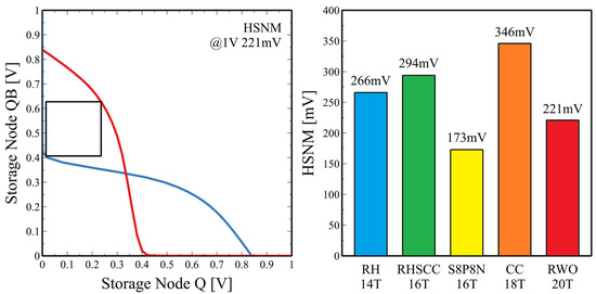
Figure 4.
Hold Static Noise Margin of the proposed cell and comparison with existing design.
3.1.2. RSNM Comparison
Under the read operation, an SRAM cell’s tolerance to data corruption is quantitatively evaluated by the Read Static Noise Margin (RSNM). In this scenario, two storage nodes are connected to BL and BLB and are therefore susceptible to voltage perturbations that can induce unwanted state changes. RSNM is determined in the same way as HSNM, except that it is measured during a read cycle [17].
For read accesses in the RWO-20T design, all access transistors are turned on, enabling both the Q–QB and S1–S0 node pairs to participate in the read operation. Notably, the pull-down cell ratio (CR) for the S1–S0 pair [(W/L)N4/(W/L)N8 and (W/L)N5/(W/L)N9 = 2.5] surpasses that of the Q–QB pair [(W/L)N0/(W/L)N10 and (W/L)N1/(W/L)N11 = 1], making the S1–S0 discharge path the dominant contributor (about 71.43%) to the read process. For this reason, the critical RSNM is measured at the S1–S0 pair. Owing to this higher CR, as illustrated in Figure 5, the RSNM achieved by the RWO-20T is 1.21×, 3.05×, 8.28×, and 6.44× that of the RH-14T, RHSCC-16T, S8P8N-16T, and CC-18T.
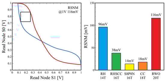
Figure 5.
Read Static Noise Margin of the proposed cell and comparison with existing design.
3.1.3. WWTV Comparison
For assessing write stability, Write Static Noise Margin (WSNM) has been frequently used, but more recent research has shown that Word Line Write Trip Voltage (WWTV) provides a more dependable criterion for evaluating the write performance of SRAM cells. Unlike traditional metrics, WWTV defines the write margin as the voltage difference between WL and VDD precisely when the storage node changes state upon WL activation [18]. Higher WWTV values indicate that successful data writing can be achieved even at reduced word line voltages, which is particularly beneficial for ensuring robust write functionality in voltage-constrained or radiation-prone environments.
In the case of the RWO-20T architecture, by incorporating NMOS transistors in the pull-up path and designing a low pull-up cell ratio (CR), the ‘1’ storage node can be written rapidly at a reduced voltage of approximately 0.8 V instead of the standard 1 V. As depicted in Figure 6, the RWO-20T exhibits WWTV values that are 6.19×, 1.42×, 1.01×, and 1.11× those of the RH-14T, RHSCC-16T, S8P8N-16T, and CC-18T.
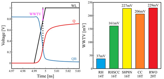
Figure 6.
Word Line Write Trip Voltage of the proposed cell and comparison with existing design.
3.2. Access Time Comparison
When evaluating the performance of SRAM, both operational stability, such as Static Noise Margin (SNM) and WWTV, and the speed at which data can be read from and written to memory cells are highly important factors. These characteristics become particularly crucial in space environments, where systems are often exposed to extreme conditions such as fluctuating temperatures, intense cosmic radiation, or frequent power supply disturbances. In such situations, rapid and accurate data access enables swift responses to unexpected events, thereby directly influencing the overall reliability and safety of the system [19].
3.2.1. Read Access Time Comparison
Read access time (RAT) represents the latency associated with sensing and outputting data from an SRAM cell during read operations. Conventionally, RAT is measured as the elapsed time from the instant when the WL voltage rises to 50% of VDD until a 50 mV voltage differential develops between the BL and BLB.
Within the RWO-20T cell, activating all access transistors during read mode enables the use of multiple parallel discharge routes involving both the Q–QB and S1–S0 nodes. This architectural feature allows BL or BLB to be pulled down more quickly compared to conventional designs. As presented in Figure 7, RWO-20T demonstrates significantly reduced RAT values, by factors of 1.66×, 1.06×, 1.80×, and 1.15×, when benchmarked against the RH-14T, RHSCC-16T, S8P8N-16T, and CC-18T, respectively.
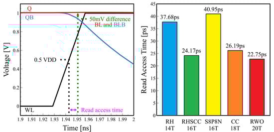
Figure 7.
Read Access Time of the proposed cell and comparison with existing design.
3.2.2. Write Access Time Comparison
The speed at which new data can overwrite the existing contents of an SRAM cell is an essential indicator of write performance, commonly referred to as the write access time (WAT). This metric is typically characterized as the duration from the point at which the WL voltage reaches 50% of the VDD to the moment when the voltages at the storage nodes Q and QB cross each other, a transition signifying the completion of data inversion.
By employing a low pull-up CR and maintaining a lower voltage at the Q–QB node pair, the RWO-20T promotes quicker switching during the write phase. These enhancements result in a substantial improvement in write speed. As indicated in Figure 8, in benchmarking against the RH-14T, RHSCC-16T, S8P8N-16T, and CC-18T cells, the RWO-20T achieves a WAT that is 1.66×, 1.06×, 1.80×, and 1.15× shorter, respectively.
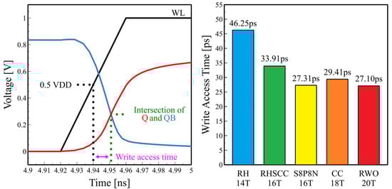
Figure 8.
Write Access Time of the proposed cell and comparison with existing design.
3.3. Soft-Error Robustness Verification and Comparison
The soft-error tolerance of an SRAM cell under radiation-induced transients can be quantitatively assessed by the critical charge (Qc), which represents the minimum amount of charge needed to flip the stored data at a sensitive node. Specifically, if an incident particle deposits more than Qc at a sensitive node, a data upset may occur. Accordingly, a higher Qc value indicates greater immunity to soft errors [20]. To simulate and determine Qc, a current pulse, typically modeled by a double-exponential function, is injected into the node of interest. The injected current can be expressed as follows:
Here, I0 indicates the peak current of the injected pulse, and Qinj represents the total charge introduced into the node. The term τα sets the characteristic time for charge collection at the junction, while τβ defines the timescale related to the initial creation of the ion track due to a particle impact. The collection time constant associated with the junction is represented by τα, having a value of 200 ps, whereas the time constant corresponding to the establishment of the initial ionization track is denoted by τβ, which is 50 ps, as reported in [3].
Figure 9 presents simulated waveforms for SEU and SEMNU, and Table 1 summarizes the recovery probabilities of each cell, defined as the ratio of the number of recoverable SEU cases to the total number of possible SEU occurrences. Figure 10 displays the simulation results for Qc. Given its high Qc and recovery probability, the RWO-20T is therefore expected to offer superior reliability in space environments.
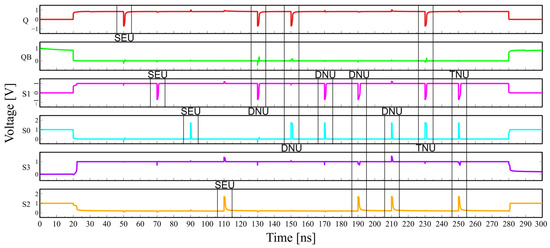
Figure 9.
Waveform demonstrating the SEU and SEMNU recovery of the proposed cell during hold operation.

Table 1.
Node recovery rate and Qc comparison.
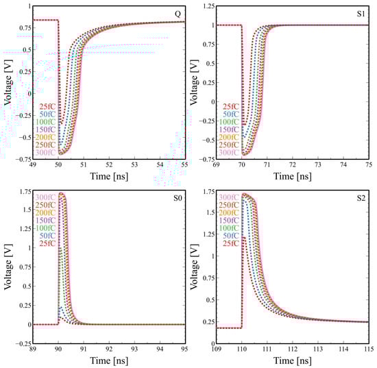
Figure 10.
Waveform demonstrating the SEU effect of the sensitive nodes.
3.4. Electric Quality Metric Comparison
A comprehensive benchmark for quantitatively assessing the overall performance of radiation-tolerant SRAM cells is provided by the Electrical Quality Metric (EQM). By consolidating multiple design parameters, including SNM, Qc, access time, and hold power consumption, these diverse characteristics are synthesized into a single representative value through EQM. This integration provides a comprehensive understanding of how the improvement of one performance aspect may influence others, thereby facilitating more balanced and optimized design decisions under complex constraints. The EQM is calculated according to the following formula.
Figure 11 illustrates the EQM comparison among the evaluated cells, while Table 2 provides the comprehensive comparison results. The proposed RWO-20T achieves values that are 122.30×, 6.11×, 7.93×, and 37.04× higher than those of the RH-14T, RHSCC-16T, S8P8N-16T, and CC-18T.
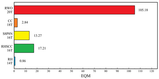
Figure 11.
Electric Quality Metric of the proposed cell and comparison with existing design.
Table 2.
Performance comparison at VDD = 1 V.
4. Conclusions
In this work, we presented the RWO-20T SRAM cell, a radiation-hardened design optimized for superior resilience and access speed in space environments. Compared to conventional RHBD cells such as RH-14T, RHSCC-16T, S8P8N-16T, and CC-18T, the RWO-20T demonstrates complete SEU immunity, strong SEMNU recovery, and leads in key performance indicators including RSNM, WWTV, critical charge, and Electrical Quality Metric (EQM). The cell achieves both faster read/write access and higher error tolerance, enabled by structural choices such as low pull-up ratios and multi-path discharging, while maintaining robust recovery even in dual- and triple-node upset scenarios.
While area and HSNM trade-offs exist due to the increased transistor count and internal complexity, RWO-20T’s significant gains in reliability, access time, and soft-error robustness make it a highly promising solution for next-generation SRAM deployed in radiation-prone, mission-critical applications. These findings highlight the value of design-level hardening strategies for dependable memory circuits in the harsh conditions of space.
Author Contributions
Conceptualization, K.-W.K., E.G.J. and S.-H.J.; methodology, K.-W.K.; validation, K.-W.K.; data curation, K.-W.K.; writing—original draft preparation, K.-W.K.; writing—review and editing, E.G.J. and S.-H.J.; visualization, K.-W.K.; supervision, E.G.J. and S.-H.J.; project administration, S.-H.J.; funding acquisition, E.G.J. All authors have read and agreed to the published version of the manuscript.
Funding
This research received no external funding.
Institutional Review Board Statement
Not applicable.
Informed Consent Statement
Not applicable.
Data Availability Statement
The original contributions presented in this study are included in the article. Further inquiries can be directed to the corresponding author.
Acknowledgments
The EDA Tool was supported by the IC Design Education Center, Republic of Korea.
Conflicts of Interest
The authors declare no conflicts of interest.
References
- Gul, W.; Shams, M.; Al-Khalili, D. SRAM Cell Design Challenges in Modern Deep Sub-Micron Technologies: An Overview. Micromachines 2022, 13, 1332. [Google Scholar] [CrossRef] [PubMed]
- Pandey, M.; Islam, A. Radiation Tolerant by Design 12-Transistor Static Random Access Memory. In Proceedings of the 2022 IEEE International Conference of Electron Devices Society Kolkata Chapter (EDKCON), Kolkata, India, 26–27 November 2022; pp. 534–539. [Google Scholar] [CrossRef]
- Pal, S.; Mohapatra, S.; Ki, W.-H.; Islam, A. Soft-Error-Aware Read-Decoupled SRAM with Multi-Node Recovery for Aerospace Applications. IEEE Trans. Circuits Syst. II Express Briefs 2021, 68, 3336–3340. [Google Scholar] [CrossRef]
- Marques, C.M.; Wrobel, F.; Aguiar, Y.Q.; Michez, A.; Saigné, F.; Boch, J.; Dilillo, L.; García Alía, R. Evaluation of a Simplified Modeling Approach for SEE Cross-Section Prediction: A Case Study of SEU on 6T SRAM Cells. Electronics 2024, 13, 1954. [Google Scholar] [CrossRef]
- Lin, S.; Kim, Y.-B.; Lombardi, F. Analysis and Design of Nanoscale CMOS Storage Elements for Single-Event Hardening with Multiple-Node Upset. IEEE Trans. Device Mater. Reliab. 2012, 12, 68–77. [Google Scholar] [CrossRef]
- Liu, C.; Liu, H.; Yang, J. A Novel Low-Power and Soft Error Recovery 10T SRAM Cell. Micromachines 2023, 14, 845. [Google Scholar] [CrossRef] [PubMed]
- Pavan Kumar, M.; Lorenzo, R. A review on radiation-hardened memory cells for space and terrestrial applications. Int. J. Circuit Theory Appl. 2023, 51, 475–499. [Google Scholar] [CrossRef]
- Leon, V.; Papatheofanous, E.A.; Lentaris, G.; Bezaitis, C.; Mastorakis, N.; Bampilis, G.; Reisis, D.; Soudris, D. Combining Fault Tolerance Techniques and COTS SoC Accelerators for Payload Processing in Space. In Proceedings of the 2022 IFIP/IEEE 30th International Conference on Very Large Scale Integration (VLSI-SOC), Patras, Greece, 3–5 October 2022; pp. 1–6. [Google Scholar] [CrossRef]
- Guo, J.; Zhu, L.; Sun, Y.; Cao, H.; Huang, H.; Wang, T.; Qi, C.; Zhang, R.; Cao, X.; Xiao, L.; et al. Design of Area-Efficient and Highly Reliable RHBD 10T Memory Cell for Aerospace Applications. IEEE Trans. Very Large Scale Integr. (VLSI) Syst. 2018, 26, 991–994. [Google Scholar] [CrossRef]
- Li, H.; Xiao, L.; Qi, C.; Li, J. Design of High-Reliability Memory Cell to Mitigate Single Event Multiple Node Upsets. IEEE Trans. Circuits Syst. I Regul. Pap. 2021, 68, 4170–4181. [Google Scholar] [CrossRef]
- Bharti, P.K.; Mekie, J. RHSCC-16T: Radiation Hardened Sextuple Cross Coupled Robust SRAM Design for Radiation Prone Environments. In Proceedings of the 2022 IEEE 40th International Conference on Computer Design (ICCD), Olympic Valley, CA, USA, 23–26 October 2022; pp. 17–24. [Google Scholar] [CrossRef]
- Bai, N.; Xiao, X.; Xu, Y.; Wang, Y.; Wang, L.; Zhou, X. Soft-Error-Aware SRAM with Multinode Upset Tolerance for Aerospace Applications. IEEE Trans. Very Large Scale Integr. (VLSI) Syst. 2024, 32, 128–136. [Google Scholar] [CrossRef]
- Cai, S.; Wen, Y.; Ouyang, J.; Wang, W.; Yu, F.; Li, B. A highly reliable and low-power cross-coupled 18T SRAM cell. Microelectron. J. 2023, 134, 105729. [Google Scholar] [CrossRef]
- Calin, T.; Nicolaidis, M.; Velazco, R. Upset Hardened Memory Design for Submicron CMOS Technology. IEEE Trans. Nucl. Sci. 1996, 43, 2874–2878. [Google Scholar] [CrossRef]
- Park, J.; Lee, S.; Jeong, H. Voltage Boosted Fail Detecting Circuit for Selective Write Assist and Cell Current Boosting for High-Density Low-Power SRAM. IEEE Trans. Circuits Syst. I Regul. Pap. 2023, 70, 797–805. [Google Scholar] [CrossRef]
- Yoon, T.; Park, J.; Jeong, H. Design of Static Random-Access Memory Cell for Fault Tolerant Digital System. Appl. Sci. 2022, 12, 11500. [Google Scholar] [CrossRef]
- Jiang, J.; Xu, Y.; Zhu, W.; Xiao, J.; Zou, S. Quadruple Cross-Coupled Latch-Based 10T and 12T SRAM Bit-Cell Designs for Highly Reliable Terrestrial Applications. IEEE Trans. Circuits Syst. I Regul. Pap. 2019, 66, 967–977. [Google Scholar] [CrossRef]
- Pal, S.; Sri, D.D.; Ki, W.H.; Islam, A. Radiation-hardened read-decoupled low-power 12T SRAM for space applications. Int. J. Circuit Theory Appl. 2021, 49, 3583–3596. [Google Scholar] [CrossRef]
- Peng, C.; Huang, J.; Liu, C.; Zhao, Q.; Xiao, S.; Wu, X.; Lin, Z.; Chen, J.; Zeng, X. Radiation-Hardened 14T SRAM Bit-Cell with Speed and Power Optimized for Space Application. IEEE Trans. Very Large Scale Integr. Syst. 2019, 27, 407–415. [Google Scholar] [CrossRef]
- Dodd, P.E.; Massengill, L.W. Basic Mechanisms and Modeling of Single-Event Upset in Digital Microelectronics. IEEE Trans. Nucl. Sci. 2003, 50, 583–602. [Google Scholar] [CrossRef]


Disclaimer/Publisher’s Note: The statements, opinions and data contained in all publications are solely those of the individual author(s) and contributor(s) and not of MDPI and/or the editor(s). MDPI and/or the editor(s) disclaim responsibility for any injury to people or property resulting from any ideas, methods, instructions or products referred to in the content. |
© 2025 by the authors. Licensee MDPI, Basel, Switzerland. This article is an open access article distributed under the terms and conditions of the Creative Commons Attribution (CC BY) license (https://creativecommons.org/licenses/by/4.0/).