1. Introduction
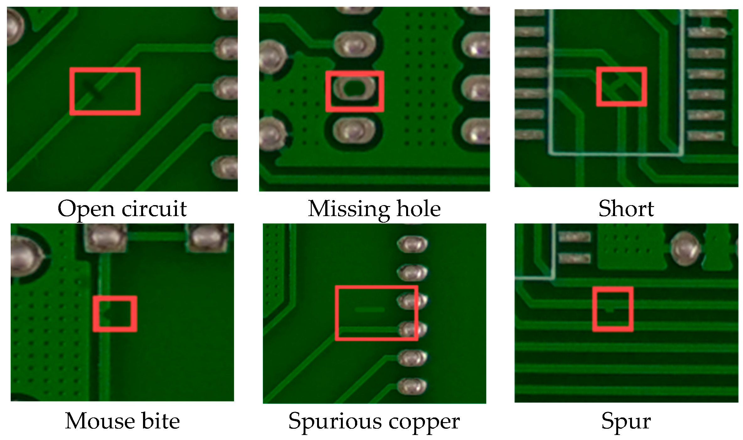
The relentless trend toward electronic miniaturization imposes ever-higher quality demands on printed circuit board (PCB) fabrication processes. As illustrated in
Figure 1, the inevitable occurrence of defects during PCB fabrication underscores the critical importance of advanced detection methodologies for maintaining stringent quality and functional standards [
1]. The traditional manual detection methods are plagued by low efficiency and subjective variability. The conventional machine learning approaches face fundamental limitations due to their dependence on handcrafted features and poor generalizability across diverse production scenarios [
2]. These challenges have propelled deep learning-based methods to the forefront of PCB defect detection research, offering superior performance through automated feature learning and enhanced adaptability to complex industrial environments.
The existing deep learning-based methods can be generally divided into two-stage networks and one-stage networks. Two-stage detectors (e.g., Faster R-CNN [
3] and Mask R-CNN [
4]) first generate candidate regions and then predict them, which have huge computational complexity and find it difficult to meet the needs of real-time detection. In contrast, single-stage detectors (including the YOLO series [
5,
6,
7,
8,
9,
10,
11,
12,
13], and RetinaNet [
14]) utilize an end-to-end detection framework that delivers substantially faster inference speeds suitable for real-time industrial applications. To overcome the limitations of baseline methods, researchers have proposed various improved versions specifically for deep learning-based PCB defect detection. Ding et al. [
15] proposed an improved Faster R–CNN framework incorporating k-means clustering [
16] for adaptive anchor box generation, which significantly boosts the small-target detection performance. Lian et al. [
17] introduced a geometric attention mechanism into Mask R–CNN architecture to improve the segmentation accuracy. Yuan et al. [
18] proposed a modified YOLOv5 framework by incorporating a HorNet backbone network and designing multi-convolution attention modules to improve small defect feature extraction. Shao et al. [
19] proposed a RetinaNet-based detection system utilizing ResNet as the feature extraction backbone. Although these methods have achieved notable progress, PCB defect detection still faces the following challenges:
- (1)
Difficulty in detecting small defects: The multi-scale convolutional downsampling operations in extraction networks inevitably lead to the degradation of critical feature information for small defects [
20], which adversely affects the precision of small defects.
- (2)
Background interference: The relentless miniaturization of electronic components necessitates ultra-dense PCB trace configurations, where the elevated complexity of background patterns and their inherent resemblance to defect features create substantial challenges for accurate defect–background differentiation.
- (3)
Trade-off between accuracy and speed: Existing PCB defect detection methods face a fundamental trade-off between accuracy and efficiency, where improvements in detection precision typically come at the expense of increased model complexity and computational overhead, which makes it challenging to achieve optimal performance in both dimensions simultaneously.
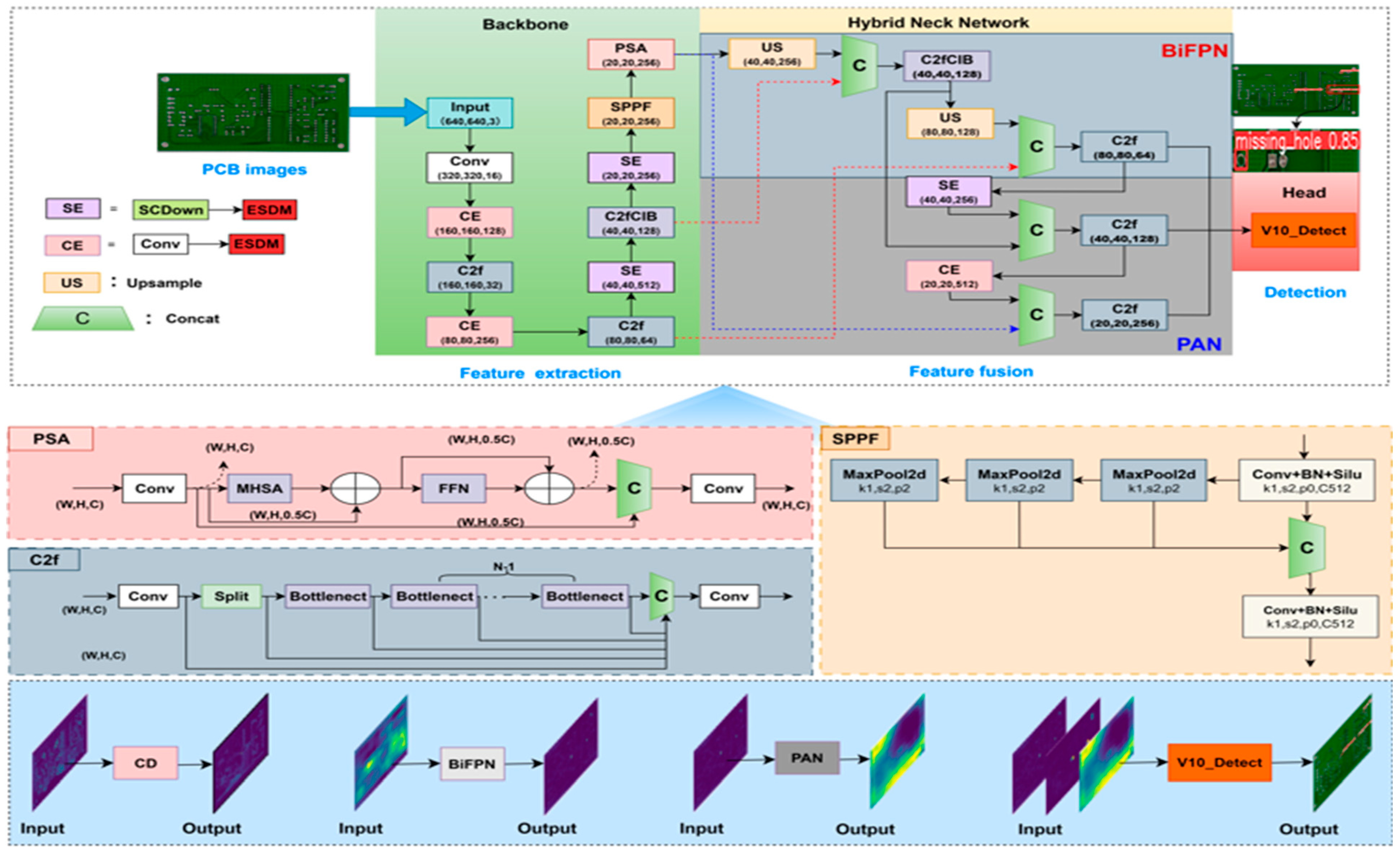
To address the above issue, we have pertinently improved and optimized the feature extraction and feature fusion of YOLOv10, respectively. The main contributions of this paper are as follows:
- (1)
A novel EH-YOLO framework based on improved YOLOv10 is proposed, which further realizes the lightweight features of the network model by ensuring the improvement of detection accuracy and speed.
- (2)
In the backbone of the network, we design ESDM, which converts the spatial information of the input information into channel information through the dual mechanism of dimension transformation and attention. The model can obtain the deep semantics while retaining the shallow semantic features, so as to improve the detection accuracy of PCB defects.
- (3)
The neck network part of the HNN is designed to trade-off inference speed and detection accuracy by combining the advantages of weighted bidirectional feature pyramid networks (BiFPNs) [
21] and path aggregation networks (PANs) [
22] to refine the work of different feature fusion layers.
The rest of the paper is organized as follows.
Section 2 briefly describes the advantages of YOLOv10 for PCB defect detection and
Section 3 details the proposed EH-YOLO model.
Section 4 validates the algorithm of this paper on public datasets and compares its performance with other algorithmic models.
2. Related Work
Owing to its efficient end-to-end processing framework, the YOLO architecture series has become a prominent solution for PCB defect detection, offering both accuracy and computational efficiency. Tang et al. [
23] optimized the backbone network of YOLOv5 to enhance feature extraction, while implementing an efficient intersection over union (EIoU) loss function to optimize bounding box regression for enhanced small defect localization. Xiao et al. [
24] enhanced YOLOv7-tiny backbone and neck components, which incorporate a coordinated attention (CA) mechanism to refine spatial channel features to achieve higher PCB detection accuracy. Lou et al. [
25] optimized the SPP module in YOLOv7 by replacing the serial channels with concurrent channels to improve the fusion speed of the image features. Xiong et al. [
26] employed GhostNet and HGNetV2 as the backbone network of YOLOv8, which reduces model parameter number and improves model inference speed. These approaches have achieved relatively good performance, but they do not effectively solve the problems of loss of feature information of small defects and the inherent trade-off between detection precision and computational efficiency.
YOLOv10, as an advanced one-stage detection framework, achieves remarkable breakthroughs in the trade-off between detection accuracy and inference speed through two key innovations. Firstly, it introduces a dual-allocation strategy that eliminates the need for non-maximum suppression (NMS) [
27], significantly reducing model inference latency. Secondly, the framework adopts an efficiency–accuracy co-design paradigm, which synergistically enhances both detection precision and processing speed. This dual optimization renders YOLOv10 particularly advantageous for PCB inspection applications. Li et al. [
28] proposed a framework based on YOLOv10 to enhance the ability to capture PCB defective features through a fine-grained feature enhancement approach with a dynamic weighting mechanism. Zheng et al. [
29] innovatively combined omni-dimensional dynamic convolution with optimized bottleneck structures, which leverage multi-dimensional kernel characteristics to amplify hierarchical feature extraction. Li et al. [
30] proposed a lightweight detection model named ASF-YOLO, which uses the adown module to recognize defects of different sizes and types, thereby effectively reducing the number of parameters. Liao et al. [
31] proposed the YOLOv10n-SFDC model, which incorporates the DualConv module, SlimFusionCSP module, and Shape-IoU loss function to improve detection accuracy. The aforementioned research has achieved certain progress in PCB defect detection, which offers a theoretical foundation for our work. However, there remains room for improvement in both detection accuracy and efficiency. Therefore, we optimize the backbone and neck networks of YOLOv10.
Feature dimensionality reduction and transformation techniques have a long-standing history in computer vision. Traditional methods such as PCA have primarily focused on data visualization. In recent years, research trends in this field have increasingly emphasized the preservation of feature structure and the interpretability of representations, which aligns closely with the design philosophy of our ESDM—we are similarly committed to maximally retaining structural information critical for detection tasks during spatial downsampling.
Regarding feature analysis, the MING method proposed by Colange et al. [
32] provides interpretable support tools for the visual exploration of multidimensional data, enabling the identification of still-entangled categories or size clusters within the feature space. Furthermore, their neighborhood graph superposition technique [
33] offers methodological support for assessing the quality of intermediate feature representations by quantifying distortion during dimensionality reduction. These techniques provide potential analytical tools for verifying whether the ESDM maintains crucial neighborhood relationships between defective and non-defective regions throughout the feature transformation process, thereby offering theoretical grounding for architectural design and supporting decision-making.
4. Experiments
4.1. Experimental Environment and Datasets
All experiments were conducted using the following software and hardware environment: a 64-bit Windows 10 operating system (Microsoft Corporation, Redmond, WA, USA), an NVIDIA GeForce RTX 4060 GPU (NVIDIA Corporation, Santa Clara, CA, USA), and a 12th Gen Intel(R) Core(TM) i5-12600KF CPU (Intel Corporation, Santa Clara, CA, USA). The deep learning framework utilized was PyTorch 1.10.0 with Python 3.9.0 as the programming language. The key training parameters were configured as follows: batch size was set to 32; the AdamW optimizer was employed; training was conducted for 300 epochs; input image size was maintained at 640 × 640; both initial learning rate (lr0) and final learning rate (lrf) were set to 0.01; weight decay was configured at 0.0005; random seed was fixed at 0; and exponential moving average (EMA = 0.9999) was enabled. The training process followed YOLOv10’s dual-label assignment strategy, with Wise-IoU employed as the loss function. For data augmentation, mosaic augmentation incorporating random affine transformations and random horizontal flipping was implemented, though this was disabled during the final 10 training epochs. During inference, preliminary filtering was performed using a confidence threshold of 0.001.
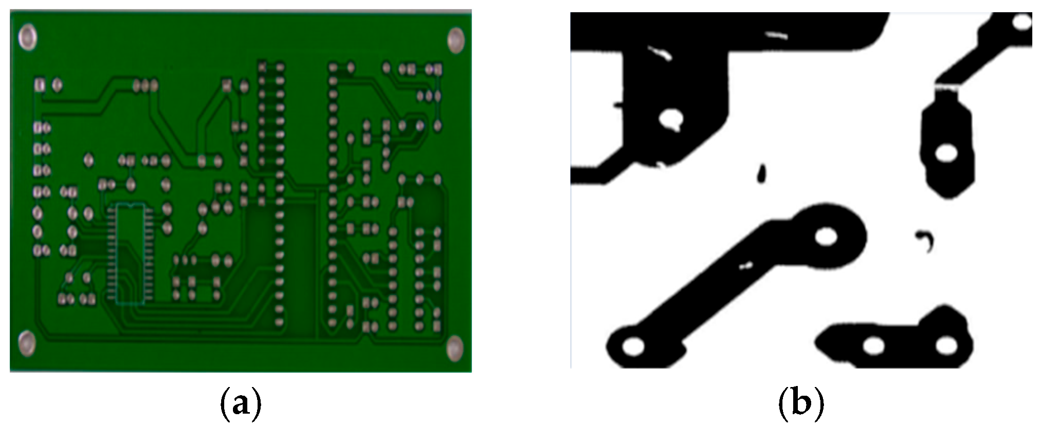
This study employs two public PCB defect detection datasets: PCB_DATASET (open-sourced by Peking University Intelligent Laboratory) and DeepPCB. As shown in
Figure 5, these two datasets exhibit significant differences in image characteristics and detection difficulty. PCB_DATASET features complex image composition with strong background interference and generally small defect targets, presenting considerable detection challenges. In contrast, the DeepPCB dataset is characterized by uniform pixel distribution, low background noise, relatively larger defect sizes, and generally easier detection. Given that both datasets predominantly contain small defects, we further categorized the defects based on their relative sizes to enable more granular evaluation: missing hole, spurious copper, and short are classified as relatively medium-sized defects (denoted as AP_M), while open circuit, spur, and mouse bite are categorized as relatively smaller defects (denoted as AP_S). To comprehensively evaluate model generalization ability and prevent evaluation bias caused by circuit board-specific information leakage, we implemented a rigorous “held-out board” partitioning strategy for both datasets. This methodology ensures that all images originating from the same physical PCB appear exclusively in either the training, validation, or test set, thereby more accurately reflecting model performance on unseen PCB instances. Both datasets were divided into training, validation, and test sets following an 8:1:1 ratio. The validation set was used exclusively for hyperparameter tuning, while the test set was solely reserved for final performance assessment, ensuring unbiased and reliable results.
4.2. Evaluation Index
This study employs recall (R), precision (P), average precision (mAP), and frames per second (FPS) for objective performance assessment. These metrics are derived from a binary classification confusion matrix, as shown in
Table 1. T
P represents correctly predicted defective samples; F
N represents defective samples incorrectly predicted as normal; F
P represents normal samples misclassified as defective; and T
N represents correctly identified normal samples.
The
R measures the model’s ability to detect defects, defined as:
The
P measures the accuracy of the model prediction results, defined as:
The
mAP computes the average prediction accuracy across all classes, defined as:
where
i represent the
i-th class and
n represents the total number of classes.
The
FPS represents how many frames of images are processed per second, defined as:
where
represents the number of photos to be processed, and
T represents the total time.
4.3. Contrast Experiment
To validate the superior performance of the EH-YOLO model, we conducted comparative experiments with several state-of-the-art models under identical experimental conditions.
As shown in
Table 2, our proposed method, EH-YOLO, demonstrates exceptional detection performance, achieving the highest accuracy among all models with a mAP@50 of 91.6% and mAP@50-95 of 45.3%. This represents a significant improvement over other strong model such as YOLOv11 (87.9%/43.1%) and YOLOv10 (84.4%/42.1%). More notably, EH-YOLO maintains balanced model complexity while achieving this performance breakthrough. With only 3.548 M parameters and 12.3 G FLOPs, it proves more efficient than larger models like Faster-R–CNN (23.59 M/38.2 G) while delivering superior detection accuracy. These results fully validate the remarkable superiority of EH-YOLO’s detection metrics, establishing its better position as a high-precision and efficient solution in the field of PCB defect detection. Furthermore, the ESDN + YOLOv11n model in the table incorporates the ESDN module into YOLOv11n, demonstrating superior detection performance compared to YOLOv11n, particularly in the improved mAP@50-95. This finding indicate that the ESDN module possesses transferability across different architectures.
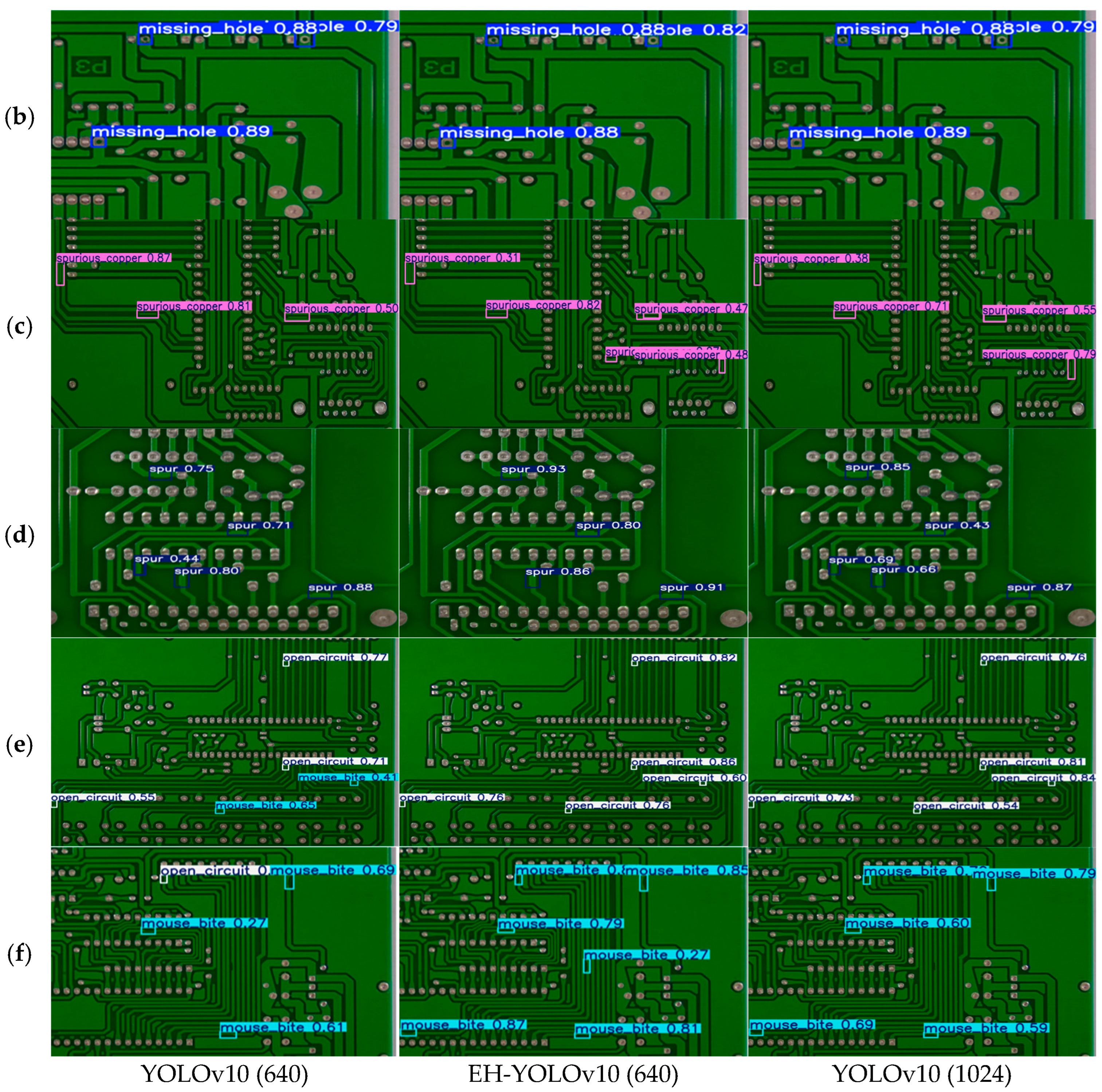
To validate the practical performance of EH-YOLO in PCB defect detection,
Figure 6 presents a comparative analysis with YOLOv10. It can be observed that with an input size of 640 × 640, YOLOv10 produces false detections when detecting small defects such as open circuit and mouse bite, while also exhibiting numerous missed detections across other defect categories. Under identical input conditions, EH-YOLO not only completely avoids both false detections and missed detections but also maintains high detection accuracy for all defect types. Furthermore, when the input size of YOLOv10 is increased to 1024 × 1024, the false detections issue is partially mitigated, although some missed detections persist. Notably, its overall detection accuracy remains lower than that of EH-YOLO. Based on the collective experimental evidence, EH-YOLO demonstrates superior performance across all PCB defect detection tasks.
4.4. Ablation Experiment
To verify the improvement of model performance by structures such as ESDM and HNN, we designed an ablation experiment. Firstly, we tested YOLOv10, then we added HNN and ESDM and verified whether they contributed to the detection. Finally, we added these improved structures in pairs and checked if there is any problem damage between them. As shown in
Table 3, compared to the baseline YOLOv10 model, with the introduction of HNN and ESDM YOLOv10 demonstrates a 1.6% and 5.9% increase in mAP@50, respectively. In group 3, the introduction of ESDM led to the increase in model parameters and the decrease in FPS, but FPS also reached 169.492, which could meet real-time detection. Experimental results in group 4 show that the ESDM effectively reduces the loss of small defect features, consequently improving feature fusion in the HNN architecture which confirms its strong compatibility.
To quantitatively assess the performance advantages of EH-YOLO in detecting minute defects, we provide a detailed precision analysis categorized by defect size and type. As shown in
Table 4, the results demonstrate that EH-YOLO achieves marked superiority over the baseline model YOLOv10 across all size categories. Specifically, it attains a 7.8% improvement in ap for small targets (AP_S), while achieving a notably greater enhancement of 13.4% for medium-sized targets (AP_M). These findings confirm that EH-YOLO not only elevates overall PCB detection accuracy but also particularly strengthens the capability to identify minute defects, thereby validating the rationality and effectiveness of our model design.
To demonstrate the generalization of the EH-YOLO model, we conducted ablation experiments on DeepPCB. The experimental results are shown in
Table 5. Obviously, each improvement contributes to an elevation in the model’s detection performance when YOLOv10 is enhanced following the methodology proposed in this work. Compared with the YOLOv10, the mAP@50 and mAP@50-95 of EH-YOLO are increased by 1.2% and 7.6%, respectively. The above experimental results can prove that EH-YOLO has the generalization property.
The above experiments demonstrate that HNN and ESDM exhibit excellent synergy, enabling EH-YOLO to significantly enhance detection accuracy while maintaining real-time performance. In addition, to further verify the feasibility and effectiveness of the various improvement schemes, a detailed experimental analysis of each improvement scheme will be conducted.
4.4.1. ESDM-Related Experiments
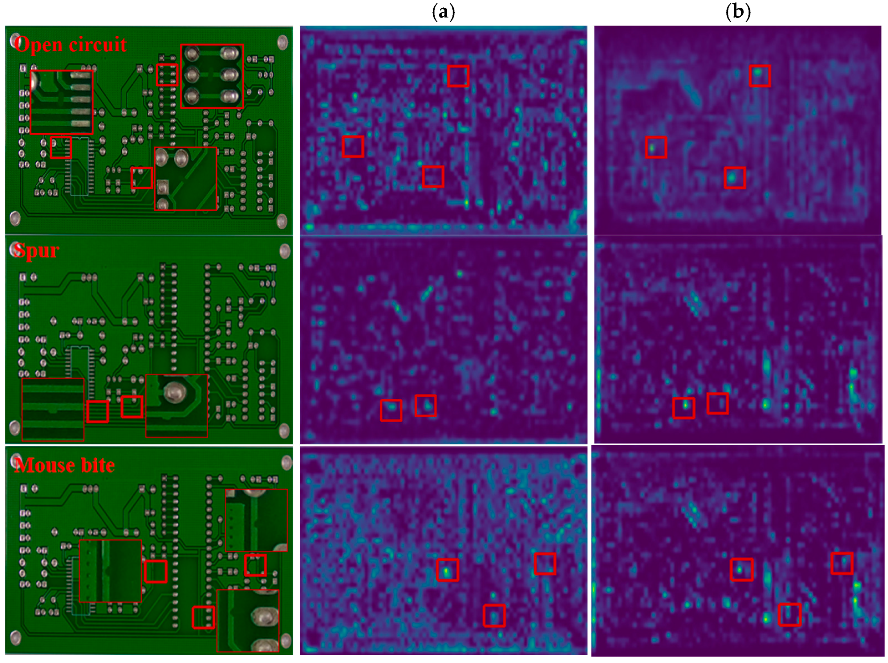
To more clearly validate the role of the ESDM in retaining fine defect features and suppressing PCB background interference, this study selects three types of PCB defects—open circuit, spur, and mouse bite, which are relatively small in size and exhibit significant background interference—for feature map visualization analysis. The results are presented in
Figure 7. Among them, (a) depicts the feature map connected to the first detection head of YOLOv10, while (b) depicts the feature map connected to the corresponding detection head of YOLOv10 after incorporating the ESDM. The comparison reveals that the feature maps generated by YOLOv10 + ESDM exhibit superior overall completeness in retaining defect information compared to the original YOLOv10. Moreover, the edge and texture characteristics of the defect regions are significantly enhanced, facilitating clearer distinction between defects and the background. This demonstrates that the ESDM achieves effective preservation of fine defect features while simultaneously suppressing interference from complex backgrounds.
Finally, it should be noted that the feature maps visualized in this experiment are those connected to the detection heads. This is because the detection heads are responsible for the final detection tasks, and the information in their feature maps most faithfully represents the model’s ultimate capacity for retaining defect-related information.
To validate the synergistic collaboration among dimensional transformation, SAM, and CAM within the ESDM, we conducted experiments. This is shown in
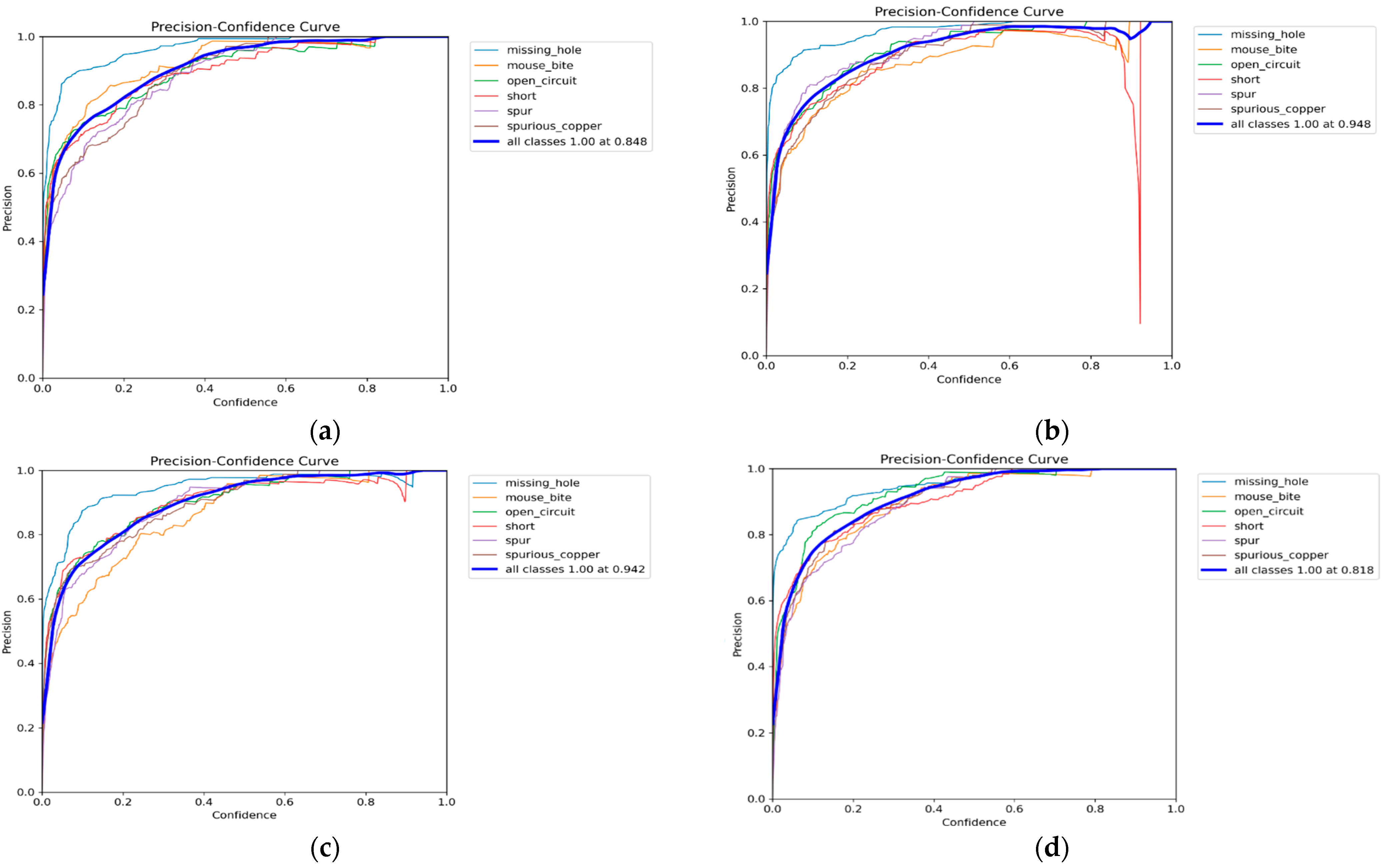
Table 6, which presents the results of YOLOv10 integrated with different ESDM configurations. In the table, 1 represents ESDM without SAM in the spatial preprocessing; 2 represents ESDM without SAM in the deep integration; 3 represents ESDM without CAM in the channel processing; and 4 represents complete ESDM implementation. Since the area under the precision–confidence (P-C) curve effectively reflects model stability,
Figure 8 gives the P-C curve of the above four different structures. Group 1 and 2 exhibit significantly lower values than group 4 across all evaluation metrics. Although group 3 achieves a 0.7% higher R value compared to group 4, it shows 1% lower P and 1.4% lower mAP@50 and with a reduced area under the P-C curve. These experimental results confirm the strong synergistic effects among dimensional transformation, SAM, and CAM within the ESDM.
4.4.2. HNN-Related Experiments
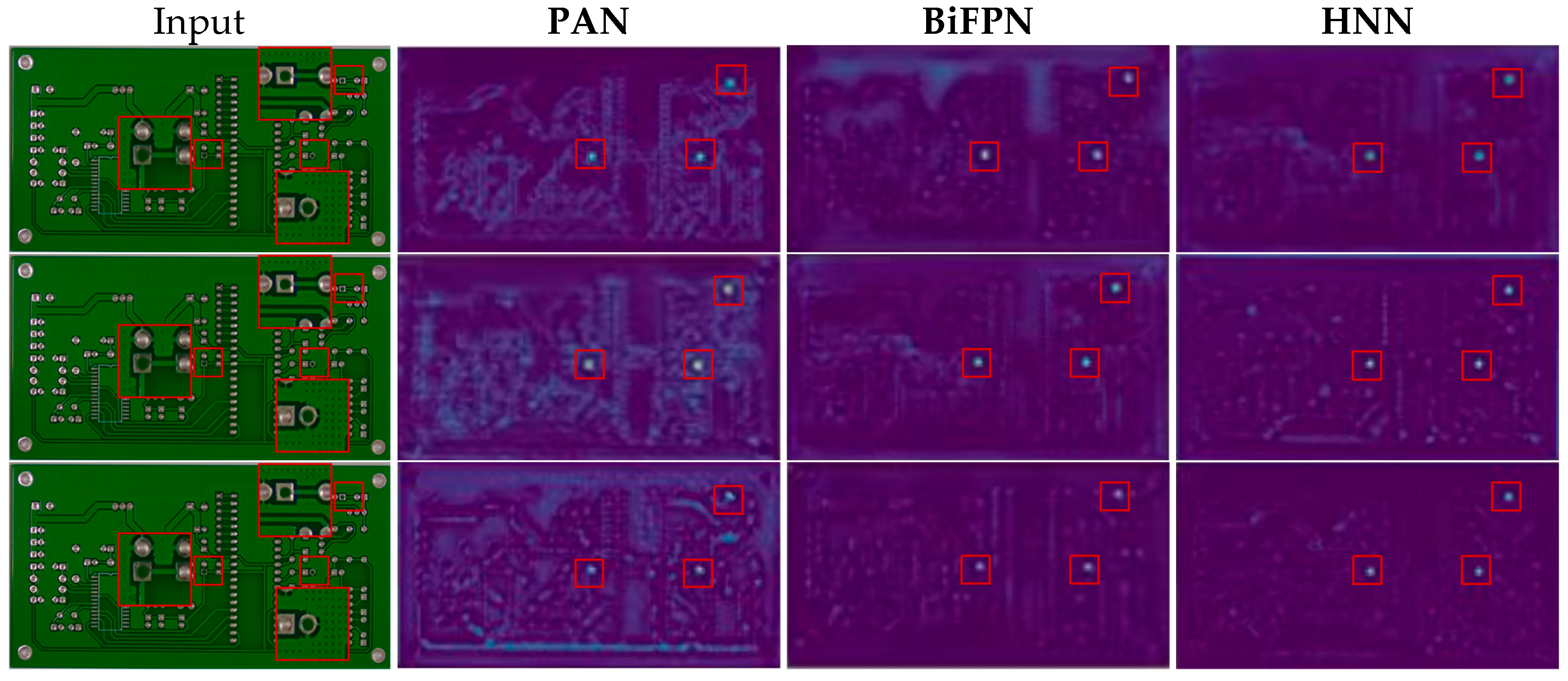
To validate the effectiveness of HNN in balancing detection accuracy and speed, we conducted comparative experiments by integrating three feature fusion architectures—PAN, BiFPN, and HNN—into the YOLOv10 baseline model. As shown in
Figure 9, PAN produces feature maps that appear blurry with poorly defined defect features while exhibiting substantial background noise. In contrast, BiFPN generates sharper feature maps with more distinct defect characteristics and reduced background interference. Our proposed HNN has clearer feature map clarity.
Table 7 reveals that PAN demonstrated the lowest efficiency, while our HNN achieved the optimal accuracy of 86.0% mAP, surpassing BiFPN by 0.4%, with only minimal computational and temporal overhead (an increase of 0.2 G FLOPs and 0.3 ms latency). In summary, HNN achieves a superior balance between speed and accuracy.
4.4.3. Error and Robustness Analysis of EH-YOLO
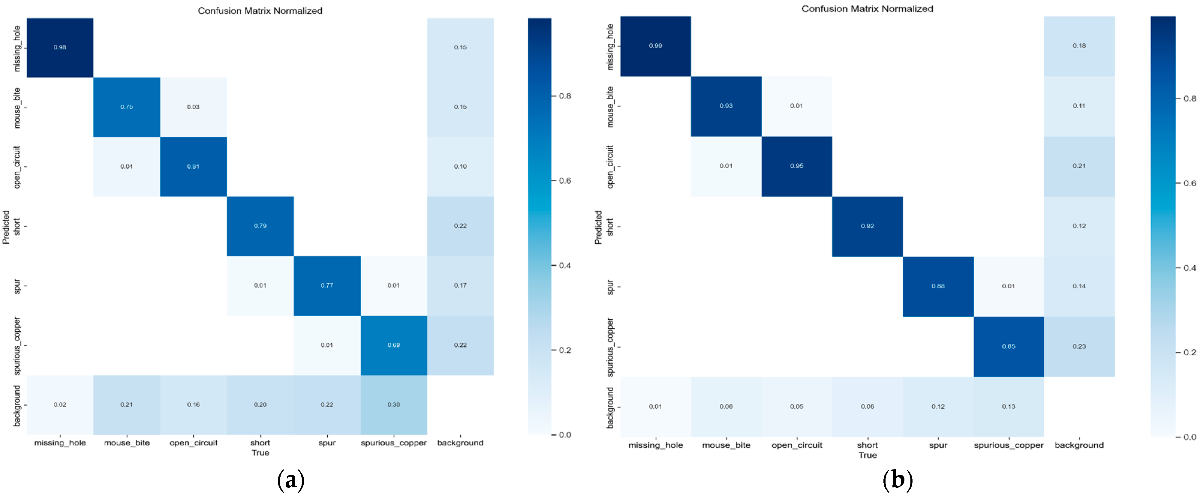
To visually demonstrate the advantage of EH-YOLO in reducing false detections,
Figure 10 presents a comparative analysis of the confusion matrices between YOLOv10 and EH-YOLO, where (a) corresponds to the results of YOLOv10 and (b) to those of EH-YOLO. It can be observed from the figure that EH-YOLO exhibits no false detections for the spur and short categories, whereas YOLOv10 demonstrates noticeable misclassifications in these cases. Furthermore, although both models occasionally misclassify open circuit as mouse bite and vice versa, the frequency of such misclassifications is significantly lower in EH-YOLO compared to YOLOv10. These results indicate that EH-YOLO achieves superior performance in suppressing false detections.
To systematically evaluate the robustness of EH-YOLO, we subjected PCB images to various perturbations including noise, illumination enhancement, and contrast adjustment. The processed images were then fed into both YOLOv10 and EH-YOLO models at a resolution of 640 × 640 for detection. As illustrated in
Figure 11, EH-YOLO maintained a consistent detection rate for missing hole defects in the AP_M category under different disturbance conditions. However, a small number of missed detections and false positives occurred when detecting open circuit defects in the AP_S category. Nevertheless, compared to the detection results of YOLOv10, EH-YOLO demonstrated significantly better overall performance across various perturbations, indicating its superior robustness.
5. Conclusions
In this paper, a novel EH-YOLO model based on YOLOv10 for PCB detection was proposed. To solve the problems of low PCB detection accuracy and background interference, we designed the ESDM, which employs dimensional transformation and multi-attention collaboration to prevent the loss of small defect features while enhancing critical feature representation. To balance the accuracy and speed of detection, we designed the HNN, which optimizes task specialization across different feature fusion layers. The superior performance of the proposed EH-YOLO model is substantiated through comprehensive evaluations on the PCB_DATASET and DeepPCB benchmarks, where it achieved mAP@50-95 scores of 45.3% and 78.8% whilst maintaining high inference speeds of 166.67 FPS and 158.73 FPS, respectively.
Although the performance of EH-YOLO for PCB detection is excellent, the results are only obtained on public datasets; therefore, the model needs to be trained more extensively. In the future, we will perform on-site collection of PCB datasets to further train the model and enhance its real-world applicability. Furthermore, we will refine the SP operation by establishing systematic mapping relationships to filter out irrelevant feature information, thereby reducing computational overhead for the model.
