Article

An Asymmetric SiC Power Module Directly Integrated with Vapor Chamber for Thermal Balancing in MMC

1
School of Electronics and Control Engineering, Chang’an University, Xi’an 710064, China
2
School of Automobile, Chang’an University, Xi’an 710064, China
3
School of Instrument Science and Engineering, Southeast University, Nanjing 210096, China
*
Authors to whom correspondence should be addressed.
Appl. Sci. 2025, 15(20), 10869; https://doi.org/10.3390/app152010869
Submission received: 3 September 2025 / Revised: 4 October 2025 / Accepted: 7 October 2025 / Published: 10 October 2025

Abstract

Featured Application

The asymmetric silicon carbide (SiC) power module directly integrated with vapor chamber (VC) can be applied to the modular multilevel converter (MMC) for thermal balancing inside the submodules (SMs). The chips of the lower side of the half bridge (HB) SM are soldered onto a VC which is added on direct bonding copper (DBC). The proposed structure can significantly reduce the hotspot temperature, maximum temperature difference and low-frequency temperature swing of the chips, thus the local over-temperature and thermal imbalance module inside the SM of SiC-MMC can be well solved.

Abstract

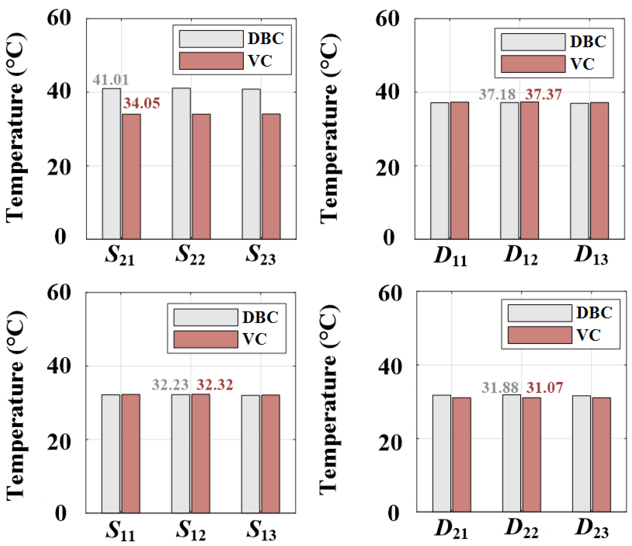
Power modules in silicon carbide (SiC)-based modular multilevel converters (MMCs) suffer from notably severe thermal imbalance and localized overheating. This paper puts forward an asymmetric SiC power module with direct integration of a vapor chamber (VC), designed to balance the thermal distribution inside MMC SMs. Specifically, the chips on the lower side of the HBSM are soldered onto a VC, which is additionally mounted on the direct bonding copper (DBC). Endowed with merits such as favorable temperature uniformity, exceptional thermal conductivity, compact size, flexible design, high integration level, and reasonable cost, the VC serves as an outstanding heat diffuser significantly expanding the effective thermal conduction area and reducing thermal resistance. Moreover, in this structure, the VC also functions as a conductor for device current. Finite element method (FEM) simulation results reveal that the proposed structure can notably reduce the hotspot temperature (from 109 ° C to 71.8 ° C ), the maximum temperature difference among chips (from 45 ° C to 13.89 ° C ), and the low-frequency temperature swing (TSL) (from 68 ° C to 38 ° C ). Consequently, the issues of localized overheating and thermal imbalance in SiC-MMC SMs are effectively addressed. Lifetime analysis further indicates that the proposed structure can reduce the annual damage rate of the chip solder layer by 92.6%.

1. Introduction

Currently, modular multilevel converters (MMCs) have emerged as one of the most appealing converters in high-voltage direct current (HVDC) transmission systems [1], high-power motor drive systems [2], and static synchronous compensators (STATCOMs) [3], thanks to their advantages of high modularity, good scalability, high efficiency, and excellent waveform quality [4,5].
Traditionally, silicon (Si)-based insulated gate bipolar transistors (IGBTs) are widely adopted in MMCs. However, the performance of such converters is constrained by the inherent theoretical limits of Si devices. As a wide bandgap (WBG) semiconductor, SiC devices exhibit superior performance compared to Si devices, including higher voltage ratings, higher operating temperatures, faster switching speeds, and lower switching losses [6]. Owing to these advantages over Si IGBTs, SiC metal-oxide-semiconductor field-effect transistors (MOSFETs) hold great potential for advancing the performance of state-of-the-art MMCs and have garnered significant attention in recent years [7]. First, the use of SiC MOSFETs can drastically reduce switching losses, thereby improving system efficiency [8]. Second, high-voltage SiC MOSFETs enable a reduction in the number of SMs, simplifying system complexity [8]. A prototype of a SiC-based MMC for medium-voltage electric machine drives has been developed in [9], and several other studies have explored issues related to SiC-MMCs, such as electromagnetic interference (EMI) reduction [8], modulation schemes [7,10], and power loss analysis [4,5]. Nevertheless, very few studies concentrate on the device-level reliability of SiC-MMCs.
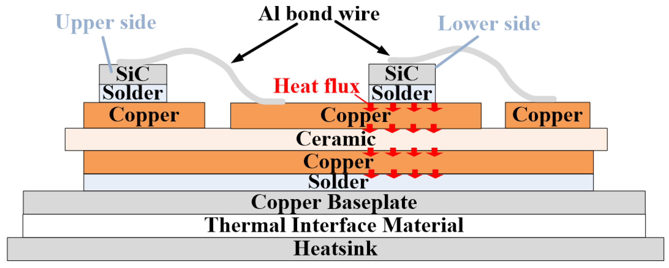
As noted in [11], when the MMC system operates at a high-power factor, the power loss distribution across power modules becomes severely unbalanced due to the inherent DC bias in arm currents. Specifically, the chips on the lower side of the HB module experience much higher heat flux and form hotspots with the highest TSL, which seriously threaten the reliability of the entire module [11]. Furthermore, as shown in Figure 1 [12], the chip size of SiC MOSFETs is significantly smaller than that of Si IGBTs with the same voltage and current ratings. According to [13], the heat flux of WBG dies can reach up to 1 kW/cm2. Therefore, when SiC-MMCs operate at high-power factors, the hotspots will exhibit extremely high heat flux. If the thermal resistance of the power module is not sufficiently low, the hotspot temperature will rise even more sharply, easily triggering thermal runaway. Although SiC MOSFETs can operate at high temperatures (typically above 200 °C), power modules with conventional packaging structures (shown in Figure 2) fail to withstand such high temperatures, as the solder layers and bond wires are prone to failure. In addition, the small size of SiC dies results in lower thermal capacitance, leading to more significant junction temperature swings. Finally, SiC is stiffer and has a much higher Young’s modulus than Si. A higher Young’s modulus causes significantly greater thermomechanical stress, more accumulated creep strain, and concentrated creep energy in the die-attached solder under the same junction temperature [14]. Thus, it is essential to resolve the issues of excessively high hotspot temperatures, large TSL, and severe thermal distribution imbalance in SiC-MMC power modules.
Numerous studies have focused on lifetime prediction for MMCs [15,16,17,18,19,20,21,22,23,24,25,26]. However, only a limited number of studies have addressed the alleviation of localized overheating and thermal imbalance in MMCs to extend their service life. In [27], an active thermal control (ATC) strategy is proposed to balance the thermal distribution in hybrid MMCs. In [28,29,30,31], device-level power loss balancing control strategies for MMCs are presented. Reference [32] argues that circulating currents affect the loss distribution of power devices and can thus be used as a control variable to indirectly regulate device temperatures. In [33,34], thermal optimization strategies for MMCs based on second-order harmonic circulating currents are proposed. In general, the uneven loss distribution in MMCs is inherent to their circuit topology. Since the DC bias in arm currents cannot be eliminated, the effectiveness of control algorithms in addressing this issue is rather limited.
Some studies have also attempted to reduce the TSL of devices in power converters. References [35,36] reduce TSL by optimizing switching losses. However, this approach is not suitable for MMCs, as switching losses account for only a small portion of the total losses in MMCs. Furthermore, in [32], the reduction in TSL is achieved at the cost of increased average junction temperature and fundamental-frequency junction temperature swing. Adaptive cooling systems proposed in [37,38,39,40] add considerable complexity and energy consumption to external cooling systems.
Therefore, optimizing the mechanical design of power modules is considered a more feasible solution to the thermal imbalance in MMCs. In [41], an air-cooled heatsink with embedded O-shaped heat pipes is designed to reduce the hotspot temperature of IGBT modules in MMCs. However, this design fails to reduce the temperature difference among chips, as the heat pipes are not integrated inside the power modules. Reference [18] indicates that using chips with higher current ratings can reduce the thermal stress on hotspots and extend their lifetime. Nevertheless, chips with higher current ratings are more costly, and excessively increasing the chip current rating is impractical given the strict size constraints of power modules. Hence, a more feasible, effective, and low-cost mechanical structure for power modules is required.
Benefiting from merits such as exceptional thermal conductivity, favorable temperature uniformity, compact size, flexible design, high integration level, and reasonable cost, VCs are ideal thermal conduction components for power modules with high local heat flux. References [42,43,44] propose replacing the copper baseplate of power modules with VCs. However, due to the considerable distance between the VC and the chip, as well as the presence of a high-thermal-resistance DBC ceramic layer in between, the reduction in the thermal resistance of the power module is not significant.
This paper proposes an asymmetric power module structure with direct vapor chamber integration, which effectively mitigates the critical challenges of localized hotspot overheating and thermal imbalance in SiC-based MMCs, thereby significantly enhancing device-level reliability and offering a robust hardware solution for high-performance power conversion systems. The remainder of this paper is organized as follows: Section 2 briefly introduces the principle of uneven loss distribution inside MMC SMs; Section 3 presents the theoretical analysis of heat transfer and the mechanical structure design; Section 4 describes the FEM simulation and lifetime analysis; Section 5 concludes the study.

2. Principle of Uneven Loss Distribution Inside the SMs of MMC

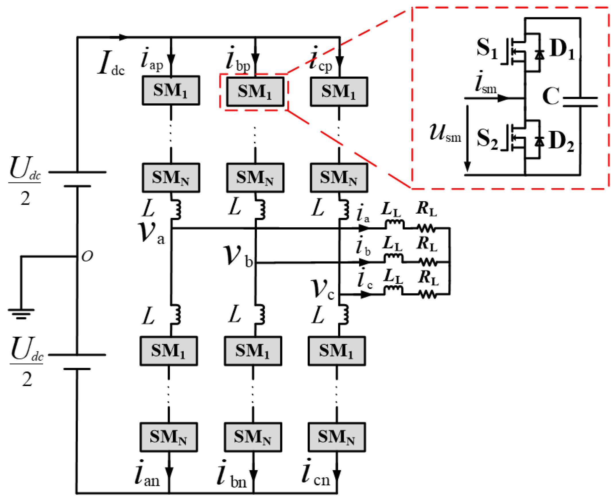
Figure 3 illustrates the schematic diagram of a three-phase SiC-MMC inverter and an HBSM. It is observable that each phase consists of an upper arm and a lower arm, and each arm comprises N HBSMs and a series-connected arm inductor. Each HBSM contains two SiC MOSFETs (S1 and S2), two anti-parallel SiC Schottky diodes (D1 and D2), and a capacitor. S1 and D1 are located on the upper side of the HBSM, while S2 and D2 are on the lower side.
The operating modes of the HBSM are shown in Figure 4 and Table 1. The HBSM operates in two distinct switching states. During the inserted mode (states B and D in Figure 4), the upper switch is turned on while the lower switch is turned off, allowing current to flow through the submodule capacitor and enabling the submodule to output the capacitor voltage. Conversely, in the bypassed mode (states A and C in Figure 4), the lower switch is turned on while the upper switch is turned off, creating an alternative current path where the capacitor is bypassed and the submodule output voltage becomes zero.
The MMC topology and operating modes of the HBSM form the basis for analyzing the uneven power loss distribution that motivates our thermal management approach.
For HBSMs based on MOSFETs, S1 and S2 stay in the off-state in Mode B and Mode C (with a gate-source voltage VGS = 5 V). When VGS = −5 V, the body diodes of the MOSFETs have a threshold voltage higher than 2 V (based on their characteristics), making it difficult to turn them on. Consequently, all current flows through the anti-parallel diodes. The reasoning underlying this design is that the equivalent resistance of the body diodes has a negative temperature coefficient, which would lead to severely uneven current distribution. Additionally, the conduction of body diodes complicates the calculation of power losses.
The ac voltage, ac current and upper arm current of phase A can be expressed as:
V a = U m sin ω t
i a = I m sin ( ω t φ )
i ap = I dc 3 + I m 2 sin ( ω t φ )
tan φ = ω L L R L
U m = I m R L 2 + ( ω L L ) 2
where U m denotes the peak value of the ac voltage, I m is the peak value of the ac current, ω is the angular frequency, φ is the phase-shift angle, I d c is the dc current, LL is the load inductance and RL is the load resistance. The arm current comprises a fundamental-frequency sinusoidal component and a DC bias. Since the circulating current suppression strategies can be applied in MMC systems, the even-order harmonics circulating current is neglected.
When the power loss is ignored, the DC-side power equals the active power on the AC side, expressed as:
U dc I dc = 3 U m 2 I m 2 cos φ
where U d c is the DC side voltage. Furthermore, the modulation index can be written as:
m = U m 0.5 U dc
Substituting Equations (6) and (7) into Equation (3), the upper arm current of phase A is:
i ap = m I m cos φ 4 + I m 2 sin ( ω t φ )
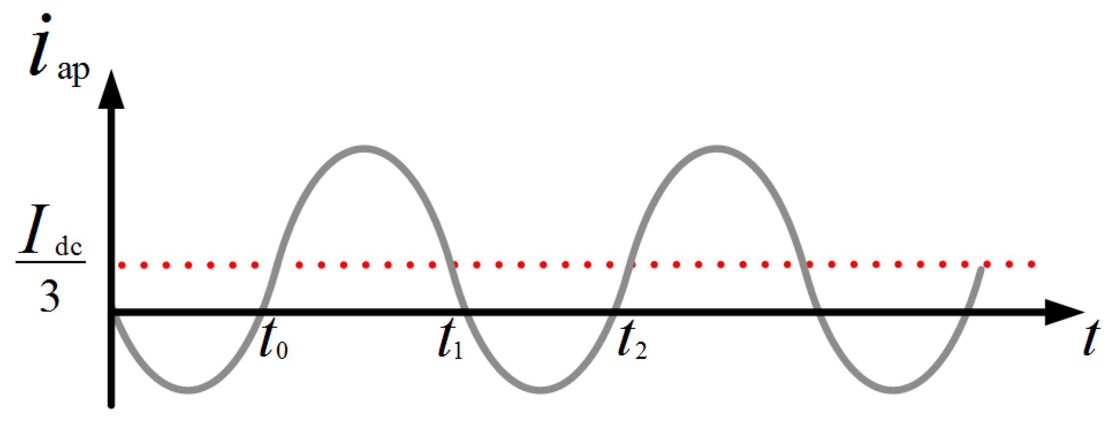
As shown in Figure 5, the arm current has zero crossing points. When i a p is positive, the current flows alternately through S2 and D1. And when i a p is negative, the current flows through D 2 and S 1 . The duration of current flow through each device can be expressed as:
t cd 1 = t 1 t 0 = π + 2 α ω ,   for   S 2   and   D 1 t cd 2 = t 2 t 1 = π 2 α ω ,   for   S 1   and   D 2
α = arcsin ( m cos φ 2 )
Unlike traction inverters, the current duration of S2 and D1 is longer than that of S1 and D2, due to the inherent DC bias in the arm current. As a result, power losses are distributed unevenly across devices, and some devices may form hotspots. According to Equation (10), thermal imbalance worsens as the power factor and modulation index increase. As most grid-connected loads are motors, taking an MMC-based high-power motor drive system as an example, thermal imbalance becomes much more severe because both cos φ and m are typically around 0.9. Moreover, if SiC power modules are used in such MMC systems, the smaller size of SiC dies will further increase the hotspot temperature. Therefore, there is an urgent need to develop a new mechanical structure for SiC-MMC power modules.

3. Theoretical Analysis of Heat Transfer and Mechanical Structural Design

3.1. Theoretical Analysis of Heat Transfer

Benefiting from merits such as exceptional thermal conductivity, favorable temperature uniformity, compact size, flexible design, high integration level, and reasonable cost, VCs are ideal thermal conduction components for power modules with high local heat flux. As shown in Figure 6, a VC consists of a metal shell with a capillary wick structure on its inner wall, and a vacuum-sealed vapor core inside. The working fluid in the vapor core absorbs heat from heat sources and vaporizes. When the vapor comes into contact with a cooler wall surface, it releases latent heat and condenses. The condensed working fluid then flows back to the heat sources via capillary force and vaporizes again. This cycle spreads concentrated heat over a much larger area, significantly expanding the effective thermal conduction area. Notably, the VC operates without requiring additional energy input. Copper columns connect the upper and lower plates of the VC, reinforcing the metal shell to withstand pressure changes in the vapor.
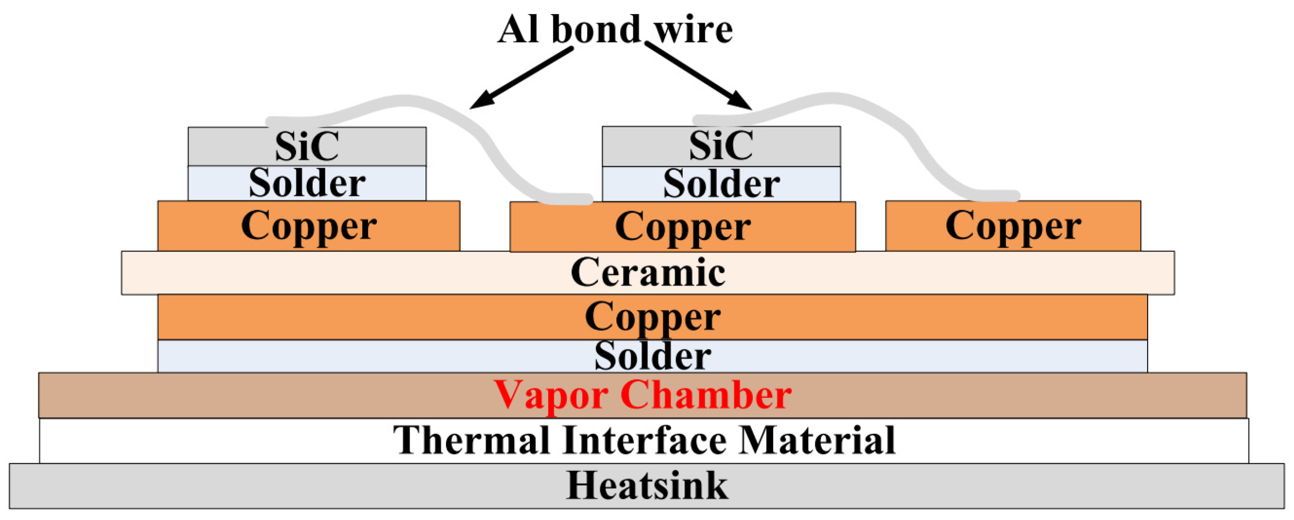
Existing research explores the use of VCs as a replacement for the copper baseplate in conventional packaging structures (shown in Figure 7). In practice, this structure only marginally improves cooling performance. The primary reason is that the VC is positioned beneath the DBC layer. Heat must first pass through the DBC before reaching the VC, preventing the VC from optimizing the heat flux distribution within the DBC layer. Additionally, the ceramic material in the DBC has inherently low thermal conductivity, resulting in a small effective heat transfer area for the ceramic layer. The thermal resistance can be expressed as
R th = d z k A ( z )
where k is the thermal conductivity, A(z) is the effective heat transfer area. Therefore, a small heat transfer area results in an increase in thermal resistance.
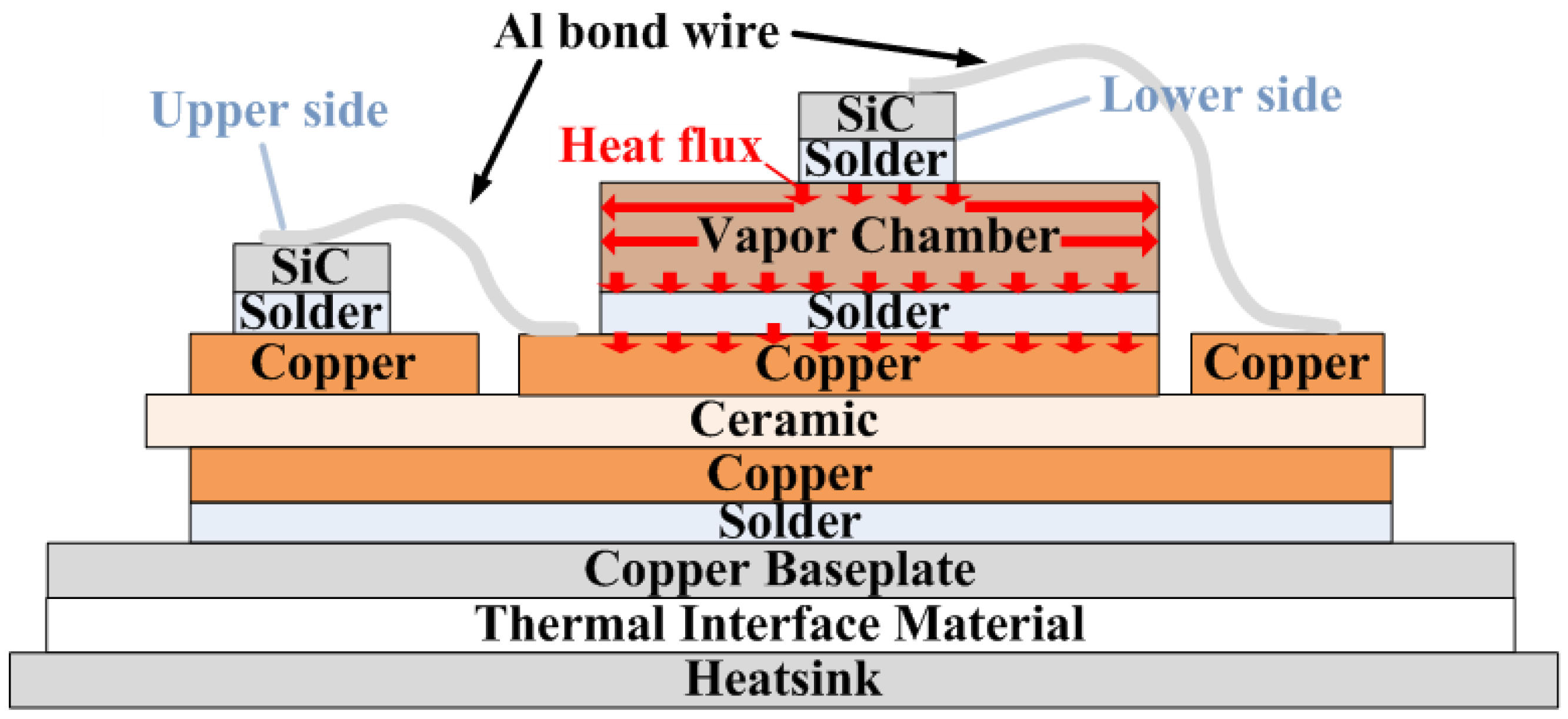
Therefore, this paper proposes a new mechanical structure (shown in Figure 8) where the VC is relocated upward. Specifically, the chip is directly soldered onto the VC, which is then soldered onto the DBC. This design aims to rapidly spread the heat generated by the chip over a larger area at an early stage, thereby expanding the effective thermal conduction area of the ceramic layer and reducing its thermal resistance. In this configuration, the VC not only acts as a heat diffuser but also functions similarly to the upper copper layer of the DBC by providing electrical conductivity. Since the VC is made of copper (which has excellent electrical conductivity), this structure is theoretically feasible.

3.2. Mechanical Structural Design of the SiC Power Module

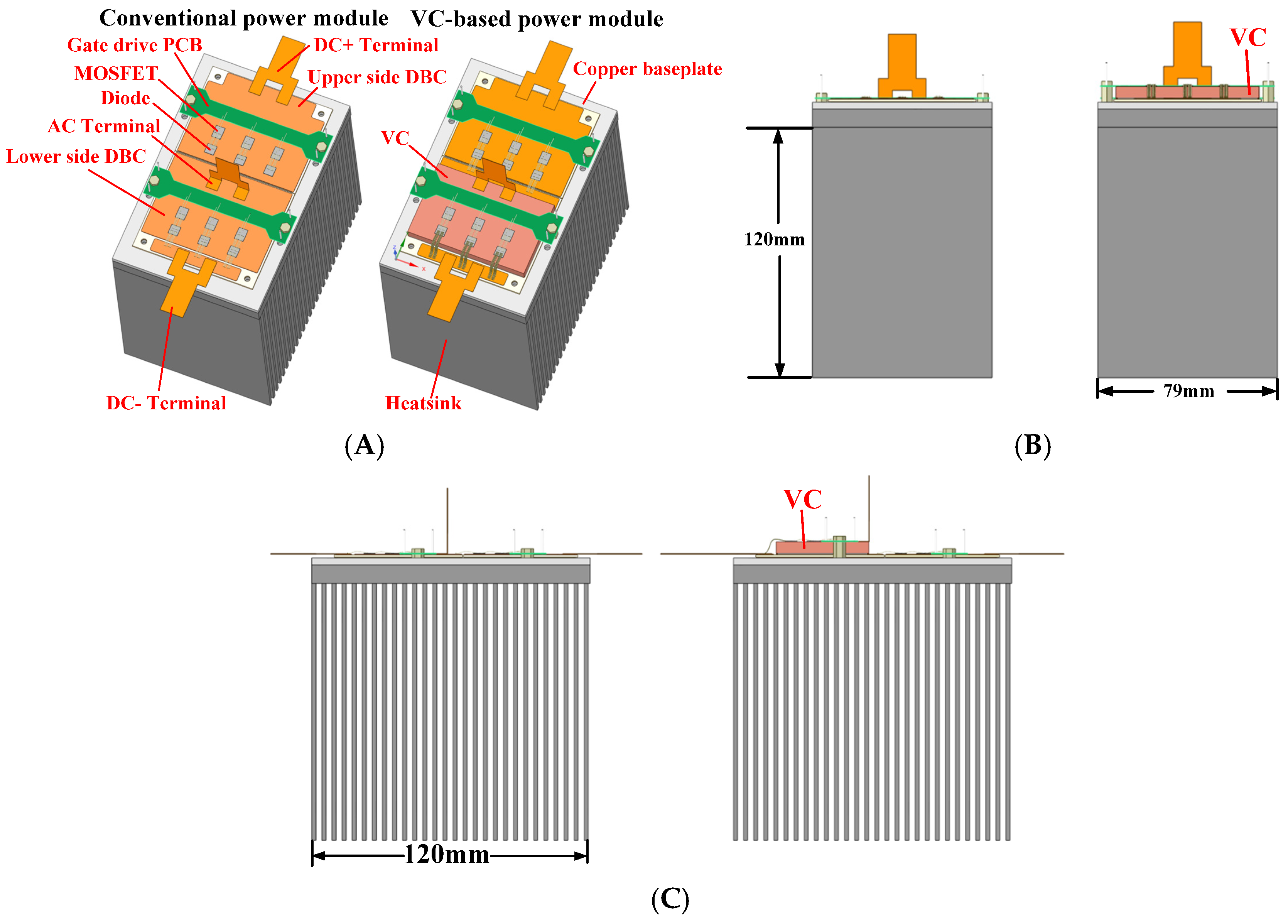
Figure 9 shows the mechanical structure of the power modules. In the proposed structure, the devices on the lower side of the HBSM are directly soldered onto a VC, which is then soldered onto the lower DBC. The parameters of the VC are listed in Table 2. Figure 10 presents a cross-sectional view of the VC’s internal structure in this study. Copper powder is sintered on the inner wall of the shell to form a wick with a porosity of 70%. The wick inside the upper copper shell (directly below the bottom switches) is thickened to 8 mm to maximize the return of working fluid to the hotspots.
The MOSFET and diode dies used in this study are the PWC020M120 and PWC70D120, respectively, both provided by Alpha Power Solutions (a Hong Kong-based semiconductor manufacturer). The sizes of the MOSFET and diode dies are 4.785 mm × 6.4 mm and 4.92 mm × 4.96 mm, respectively. The sizes of the upper and lower DBCs are 65 mm × 49.29 mm and 65 mm × 55.49 mm, respectively. The copper baseplate has a size of 79 mm × 120 mm. Gate drive PCBs are mounted on the top of the VC or DBC, and bond wires establish electrical connections between the upper surface of the dies and the upper surface of the DBC or gate drive PCBs.

4. Thermal Simulation and Lifetime Analysis

4.1. Three-Dimensional Model of the Power Module

Figure 11 shows the 3D model of the power module used for FEM simulation. The effective thermal conductivities of the wick and vapor core are 50 W/(m·K) and 50,000 W/(m·K), respectively [45]. The properties of the power module’s packaging materials are listed in Table 3. The thermal interface material (TIM) is labeled in Figure 2, Figure 7 and Figure 8.
The heatsink is made of aluminum, with its size shown in Figure 11. The fin pitch and thickness are 2.6 mm and 1.75 mm, respectively. The frontal area of the heatsink (120 mm × 120 mm) is designed to match the frontal profile of the fan.

4.2. Mission Profiles of MMC System and Power Devices

To determine the average power loss of the chips, the mission profiles of the devices must first be obtained.
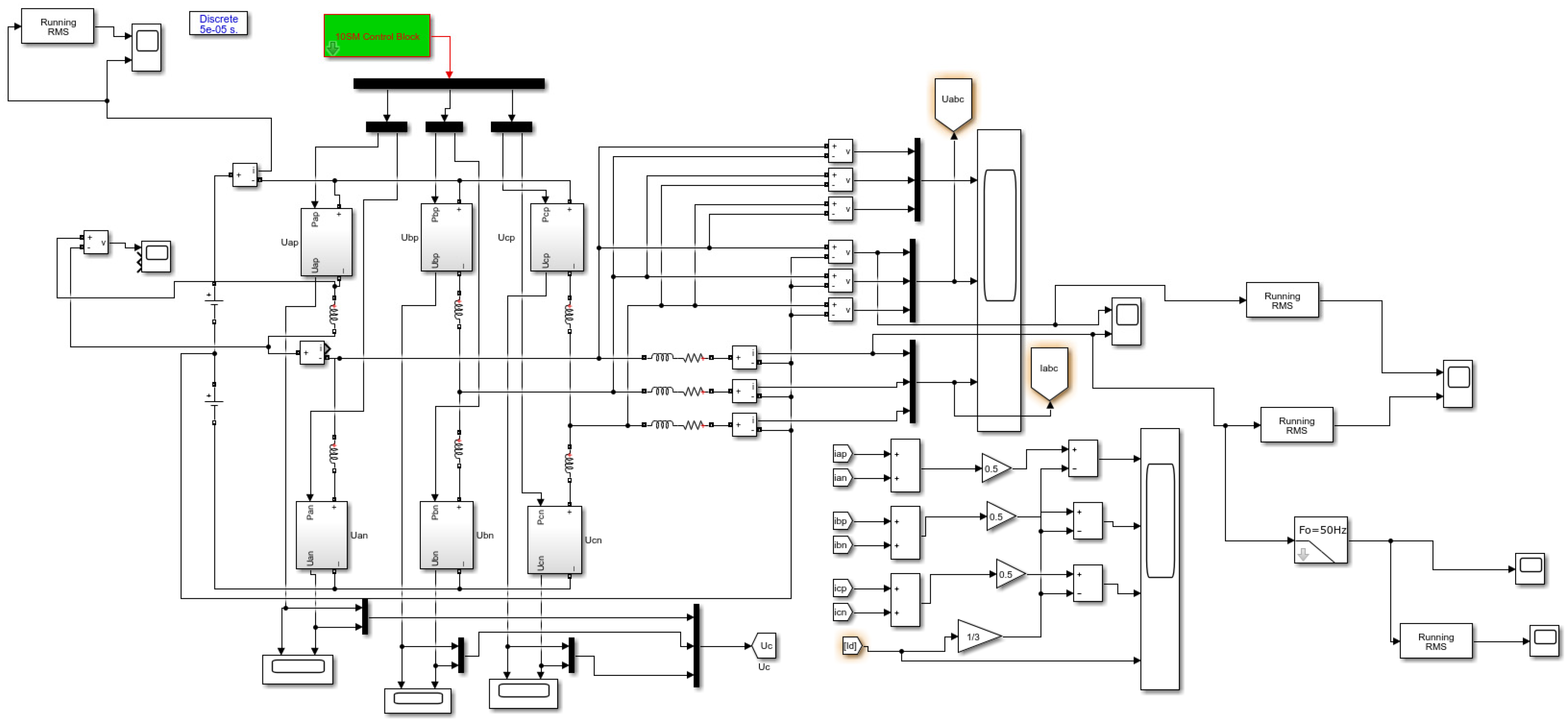
A simulation model of the MMC inverter (shown in Figure 3) was built in MATLAB v2018 Simulink to acquire the device mission profiles. The schematic diagram of the MATLAB–Simulink model is shown in Figure 12. The system parameters are listed in Table 4. The model uses a voltage outer loop controller and a current inner loop controller, with carrier phase-shift pulse width modulation (CPS-PWM) as the modulation scheme.
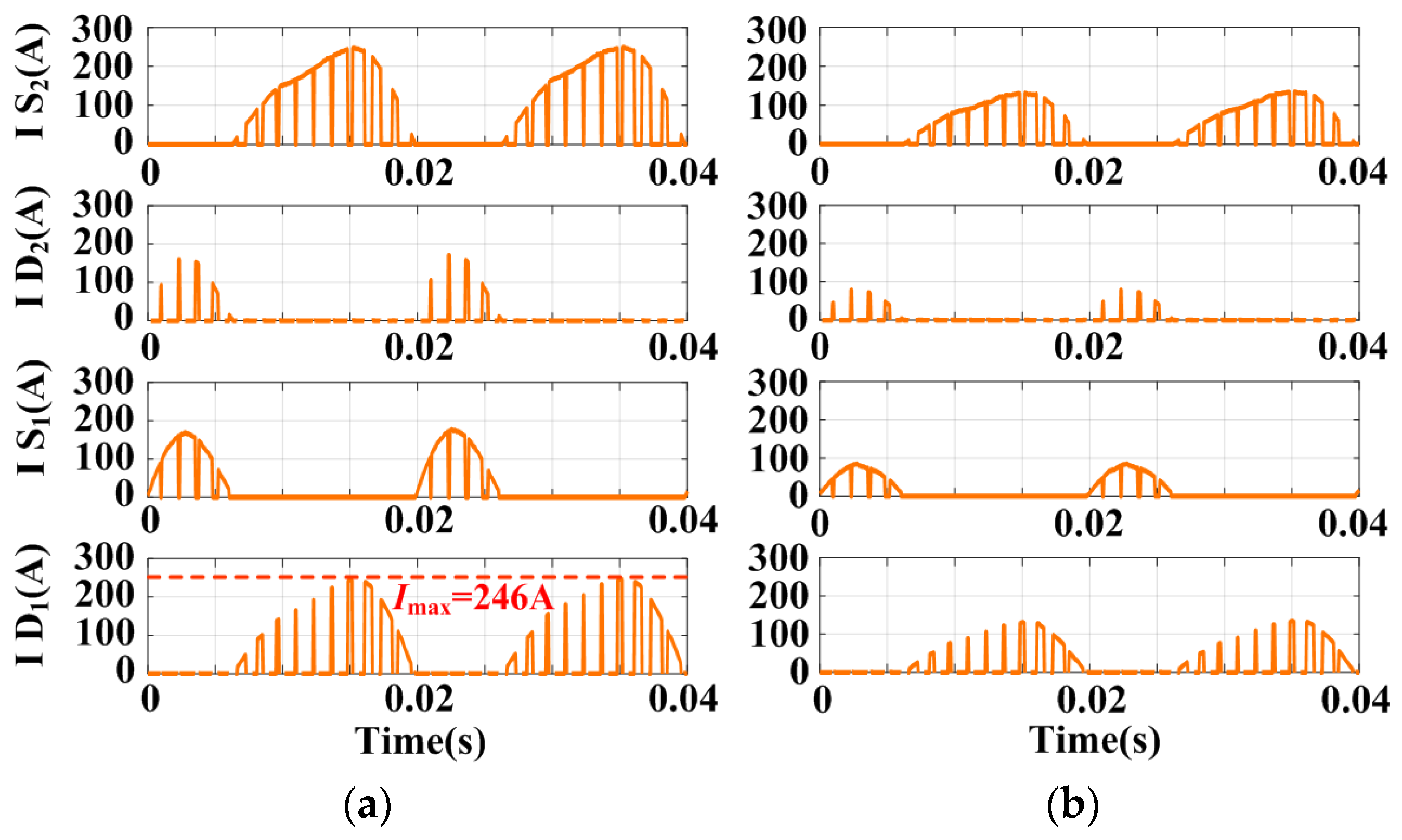
Figure 13 shows the one-day apparent power profile of the MMC inverter [16]. This curve aligns with typical human activity patterns, confirming the rationality of its design. Smax denotes the apparent power of the MMC inverter under the operating conditions listed in Table 4. Figure 14a shows the device currents of the MMC inverter at Smax. Since the DC voltage and modulation index are constant in this study, the amplitude of the AC voltage is also constant (per Equation (7)). Thus, according to Equation (6), an apparent power of 0.5Smax is achieved by reducing the AC current by 50% (i.e., doubling the load impedance in Table 4). Figure 14b shows the device currents of the MMC inverter at 0.5Smax. Current data from both full-power (Smax) and half-power (0.5Smax) operating conditions were employed to calculate the corresponding power device losses, thereby facilitating subsequent thermal simulations to obtain the junction temperatures under these respective conditions.

4.3. Heat Sources Calculation

This section presents the calculation of the average power loss of the dies, which is used for steady-state FEM thermal simulation in the subsequent section.
As shown in Figure 9, each device in the HB module consists of three parallel dies. The current distribution across the parallel dies is assumed to be uniform, for the following reasons:
(1)
The power module exhibits high symmetry in terms of terminal shape/position and chip layout.
(2)
Reference [46] points out that the positive temperature coefficient of the on-resistance (Ron) of SiC MOSFETs balances the static current across parallel devices.
(3)
Unbalanced dynamic current distribution is more likely to occur in high-switching-frequency applications [46]. However, MMCs operate at relatively low switching frequencies.
(4)
This study focuses on the temperature uniformity of the four devices in the HB module, rather than that of the parallel dies.
(5)
The paralleled chips are from the same production batch.
The average power loss of SiC MOSFET can be expressed as:
P = I RMS 2 R on ( T j ) + E SW T
where I R M S is the root mean square values of the die current (obtained from MATLAB), R o n ( T j ) is the on-resistance of the SiC MOSFET (obtained from the R o n T j curve in the manufacturer’s datasheet), T is the fundamental period and E s w is the switching loss of the SiC MOSFET, expressed as:
E SW = E SW @ T REF ( i ) ( U SM U DC @ REF ) K 1 [ 1 + K 2 ( T j T REF ) ]
where i is the instantaneous chip current at the start of the turn-off process or the end of the turn-on process (obtained from Figure 14), U D C @ r e f is the nominal test voltage (600 V, per the datasheet), U S M is the SM capacitor voltage (600 V, per Table 4). Since switching losses account for only a small portion of the total losses in SiC-MMCs and the junction temperature has a negligible impact on the switching losses of the PWC020M120, the switching loss calculation can be simplified to:
E SW = E SW @ 25 ° C ( i )
where E s w @ 25   ° C i is obtained from the E o n / E o f f I D S curves in the datasheet. As shown in Figure 14, the maximum instantaneous current of a single diode die is 82 A. According to the forward characteristics of the PWC70D120 at 75 ° C , the forward voltage is 1.8 V, lower than the threshold voltage of the body diode (as discussed in Section 2). Thus, the body diodes of the SiC MOSFETs do not conduct under this operating condition. The average power loss of the SiC Schottky diode is expressed as:
p D = I AV [ U cond @ T REF + K 3 ( T j T REF ) ] + I RMS 2 [ r cond @ T REF + K 4 ( T j T REF ) ]
where I a v is the average value of the die current (obtained from MATLAB). U c o n d @ T r e f , r c o n d @ T r e f , K 3 and K 4 are the coefficients derived from the forward characteristics of PWC70D120 (listed in Table 5). The reverse recovery loss of the SiC Schottky diode is neglected.

4.4. FEM Simulation

A square simulated fan (120 mm × 120 mm) was included in the FEM simulation, with its front aligned with the windward side of the heatsink (and no gap between them). The fan flow rate is 35 CFM, and the ambient temperature is 20 ° C . In practical applications, power modules are encapsulated with silica gel for electrical insulation. Thus, the upper surface of the power module is set as adiabatic in the thermal simulation. The chips are treated as heat sources with the calculated average power losses.
The electrothermal coupling effect refers to the significant impact of junction temperature on the on-resistance of SiC MOSFETs and the forward characteristics of SiC Schottky diodes. To ensure accurate simulation results, the influence of junction temperature is considered in power loss calculations. Specifically, power loss calculation and thermal simulation are performed iteratively. The device characteristics used for power loss calculation are continuously corrected based on the calculated junction temperature. The iteration stops when the difference between the calculated junction temperature and the temperature corresponding to the used characteristics is less than 0.5 ° C .
Figure 15 shows the average power losses of the dies. The power loss distribution is more unbalanced at Smax than at 0.5Smax. Additionally, the power loss of S2 in the VC-based power module is lower than that in the conventional power module, due to the reduced on-resistance.
Figure 16 shows the temperature contours of the two power modules at Smax. Figure 17 presents the junction temperatures of the dies at Smax. The conventional power module exhibits severe thermal imbalance, with dies S21~S23 forming hotspots (hotspot temperature of 109 ° C , much higher than that of other dies) and a maximum temperature difference of 45 ° C across the dies. By adding a VC between the bottom devices and the DBC, the temperature of S21~S23 is reduced to approximately 71.8 ° C (the largest temperature reduction among all devices), achieving localized cooling enhancement. In the VC-based module, the hotspots shift to D11~D13 (hotspot temperature of 73.5 ° C , close to that of S21~S23). Furthermore, the junction temperature of D21~D23 is close to that of S11~S13, and the maximum temperature difference across the dies is reduced to 13.89 ° C . Thus, the proposed structure achieves thermal balance between the upper and bottom devices in the MMC power module.
Figure 18 shows the thermal distribution of the DBC in the two power modules. The DBC in the conventional power module has a significantly large in-plane temperature gradient, whereas the VC-based power module exhibits a much more uniform temperature distribution on the DBC, confirming that the VC significantly expands the effective thermal conduction area of the DBC.
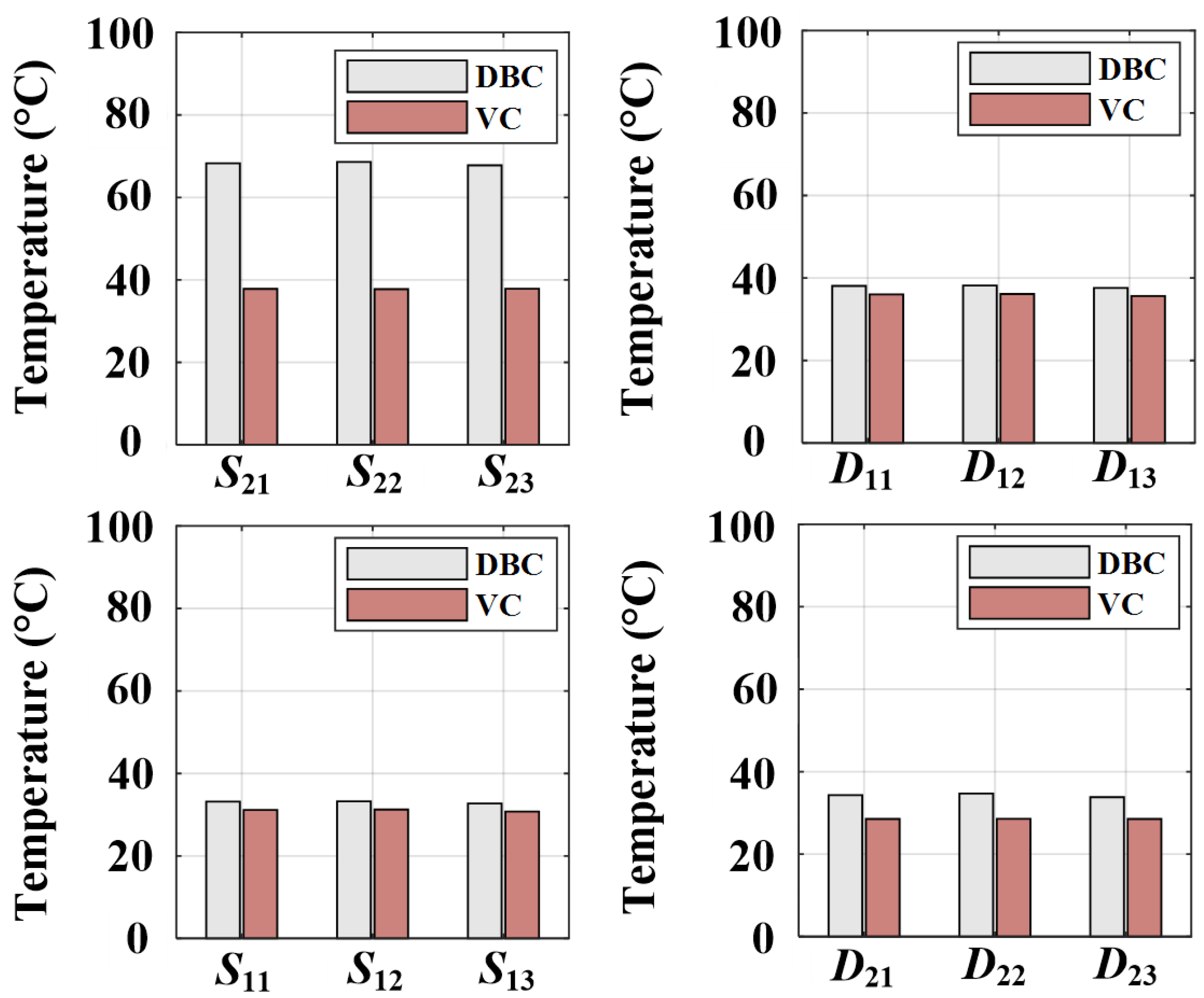
Figure 19 shows the temperature contours of the two power modules at 0.5Smax, and Figure 20 presents the junction temperatures of the dies at 0.5Smax. The TSL (calculated as the difference between the corresponding data in Figure 17 and Figure 20) is shown in Figure 21. It is evident that the dies S21~S23 in the conventional power module have the largest TSL.

4.5. Lifetime Analysis

The service life of the submodule is paramount, as it directly impacts the maintenance strategy, operational availability, and overall lifecycle cost of the MMC system.
According to [47,48], the temperature cycle with heating time (the period where power losses are generated in the IGBT resulting in a temperature swing) below 1 min has a significant effect on the fatigue of bond wires, while a much longer heating time will be more likely to induce the solder fatigue. And according to [49], thermal cycles with periods larger than 3 h cause much more annual damage (AD) in chip solder than baseplate solder. The period of the TSL in this paper is one day. Hence, the solder lifetime model is used to calculate the AD caused by the TSL. The Coffin-Manson law [50,51,52], which estimates the fatigue life according to plastic strain, is selected in this paper since it is widely accepted and considers the size of the solder layer. The model is given in the following equation:
N f = 0.5 ( L Δ α Δ T j γ χ ) 1 c
where Nf is the number of power cycles, L is the diagonal length of the chip solder joint, α is the CTE mismatch between the upper and lower plate (12.6   × 10 6   for SiC and Cu, regardless of whether the chip is soldered onto a VC or a DBC substrate, the materials on both sides of the solder joint remain SiC and Cu), T is the temperature swing shown in Figure 20, x is the thickness of the solder layer shown in Table 3, c = 0.229 is the fatigue exponent and γ = 0.606 is the ductility factor of the solder [52]. According to the Miner’s rule [53], the AD can be calculated as
A D = n N f
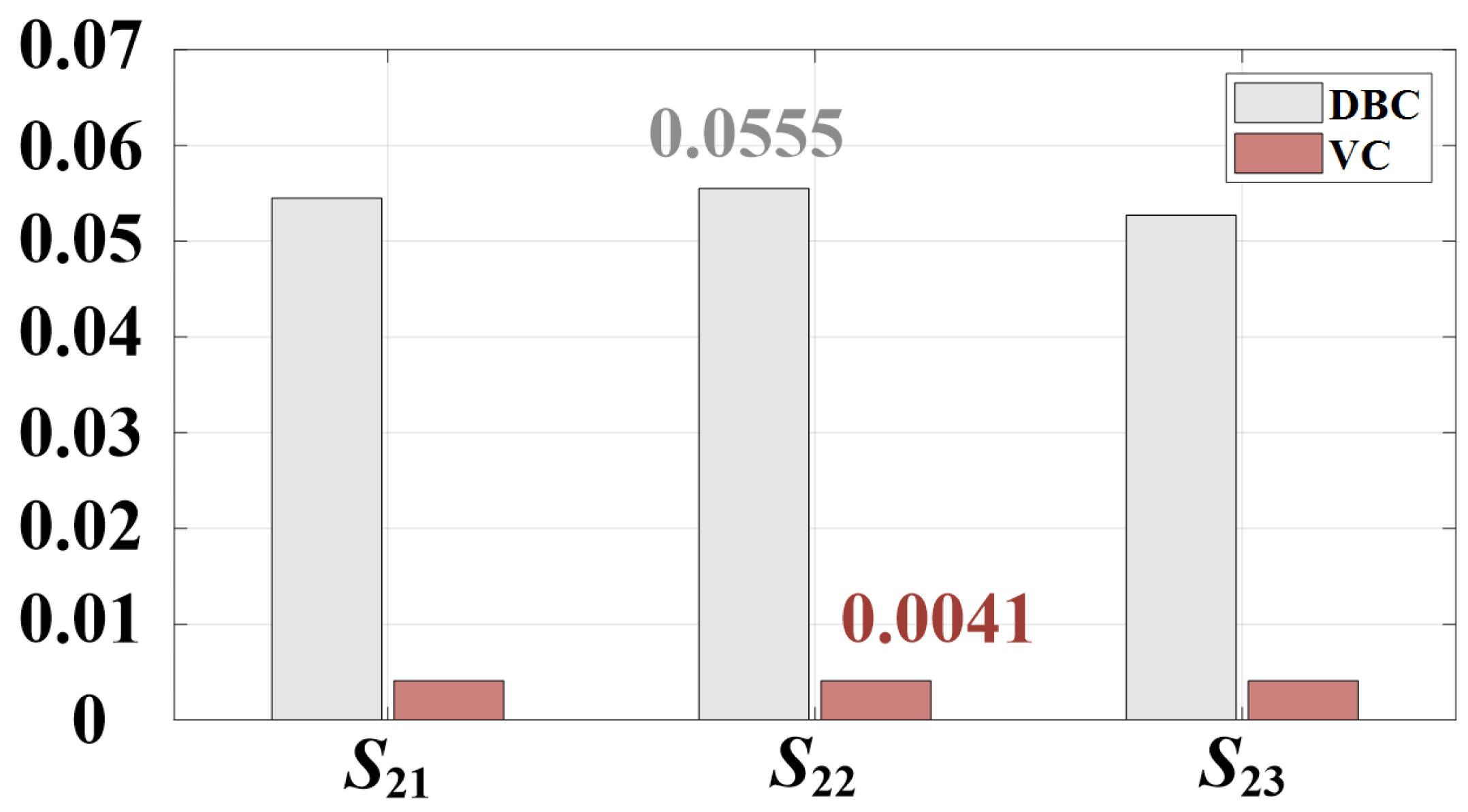
where n is the number of cycles in a year for the same stress. In conventional power modules, the lower-arm MOSFET (S21~S23) experiences the highest junction temperature and TSL, making it the lifetime bottleneck of the power module. Therefore, its AD is the focus of this study, and the calculated results are shown in Figure 22. The maximum annual damage values for the two power module types are 0.0555 and 0.0041, respectively. This demonstrates that employing VC can reduce the maximum annual damage of the chip solder joint by 92.6%, extending the service life of the solder joint by more than tenfold.

5. Conclusions

This paper proposes an asymmetric SiC power module with direct VC integration, designed to balance the thermal distribution inside MMC SMs. The chips on the lower side of the HBSM are soldered onto a VC, which is mounted on the DBC. The VC serves as an excellent heat diffuser, significantly expanding the effective thermal conduction area and reducing thermal resistance. It also conducts device current in this structure. FEM simulation results demonstrate that the proposed structure can notably reduce the hotspot temperature, the maximum temperature difference among chips, and the TSL. The hotspot temperature is reduced from 109 ° C to 71.8 ° C , the maximum temperature difference is reduced from 45 ° C to 13.89 ° C , and the TSL is reduced from 68 ° C to 38 ° C . Thus, the issues of localized overheating and thermal imbalance in SiC-MMC power modules are effectively resolved. Lifetime analysis further demonstrates that the VC can achieve a 92.6% reduction in annual damage to the chip solder joint.

Author Contributions

B.W.: Responsible for the mechanical structure design and hardware fabrication of the asymmetric SiC power module, and took the lead in drafting and revising the manuscript. X.Z.: Designed the control algorithm for the MMC, including the voltage outer loop and current inner loop controller, and optimized the carrier phase-shift pulse width modulation (CPS-PWM) scheme. Y.Z.: Participated in the analysis of the applicability of the proposed SiC power module in MMC-based high-power motor drive scenarios (relevant to automotive engineering), and assisted in organizing and verifying the experimental data of power module thermal performance. M.Q.: Conducted the finite element method (FEM) thermal simulation of the power module, including the establishment of the 3D thermal model, setting of simulation parameters (e.g., fan flow rate, ambient temperature), and analysis of temperature contour and junction temperature data. H.L.: Responsible for the performance testing experiments of the fabricated SiC power module, including thermal cycle testing, electrical performance verification (e.g., on-resistance measurement), and validation of the thermal balance effect. B.Y.: Provided overall guidance on the research direction, including the innovation design of the VC-integrated power module structure and the optimization of the thermal simulation scheme, and reviewed the manuscript. S.H.: Assisted in the calibration of parameters for the heat transfer model of the vapor chamber (VC) and the sorting of packaging material property data (e.g., thermal conductivity, specific heat), and participated in the collation of references. X.W.: Built the MMC inverter simulation model in MATLAB–Simulink, obtained the mission profiles of power devices, and calculated the average power loss of dies. Q.W.: Guided the theoretical analysis of uneven loss distribution in MMC SMs and the derivation of mathematical models (e.g., arm current, power loss formulas), and provided suggestions for improving the reliability of the power module. W.L.: Analyzed the heat transfer mechanism of the VC-based power module, including the working principle of VC (vaporization–condensation cycle) and the calculation of effective thermal conduction area, and optimized the thermal resistance reduction scheme of the DBC layer. All authors have read and agreed to the published version of the manuscript.

Funding

This work was supported by the Fundamental Research Funds for the Central Universities, Chang’an University (CHD), under Grant 300102324101, the National Natural Science Foundation of China (No. 12172064), and the Innovation and entrepreneurship training program for college students from Chang’an University entitled “Research and development of AC Electrothermal Microfluidic Immunoassay Device”.

Data Availability Statement

The data that support the findings of this study are available from the corresponding author upon reasonable request.

Conflicts of Interest

The authors declare no conflicts of interest.

Abbreviations

SiC, silicon carbide; MMC, modular multilevel converter; VC, vapor chamber; DBC, direct bonding copper; HB, half bridge; TSL, low-frequency temperature swing; AD, annual damages; FEM, finite element; STATCOMs, static synchronous compensators; SM, submodule; ATC, active thermal control; CPS-PWM, carrier phase-shift pulse width modulation.

References

  1. Alyami, H.; Mohamed, Y. Review and development of MMC employed in VSC-HVDC systems. In Proceedings of the 2017 IEEE 30th Canadian Conference on Electrical and Computer Engineering (CCECE), Windsor, ON, Canada, 30 April–3 May 2017; pp. 1–6. [Google Scholar]
  2. Song, S.; Liu, J.; Ouyang, S.; Chen, X. An improved high-frequency common-mode voltage injection method in modular multilevel converter in motor drive application. In Proceedings of the 2018 IEEE Applied Power Electronics Conference and Exposition (APEC), San Antonio, TX, USA, 4–8 March 2018; pp. 2496–2500. [Google Scholar]
  3. Farias, J.V.M.; Cupertino, A.F.; Ferreira, V.D.N.; Pereira, H.A.; Seleme, S.I.; Teodorescu, R. Reliability-Oriented Design of Modular Multilevel Converters for Medium-Voltage STATCOM. IEEE Trans. Ind. Electron. 2020, 67, 6206–6214. [Google Scholar] [CrossRef]
  4. Wu, L.; Qin, J.; Saeedifard, M.; Wasynczuk, O.; Shenai, K. Efficiency Evaluation of the Modular Multilevel Converter Based on Si and SiC Switching Devices for Medium/High-Voltage Applications. IEEE Trans. Electron Devices 2015, 62, 286–293. [Google Scholar] [CrossRef]
  5. Xu, C.; He, J.; Lin, L. Research on Capacitor-Switching Semi-Full-Bridge Submodule of Modular Multilevel Converter Using Si-IGBT and SiC-MOSFET. IEEE J. Emerg. Sel. Top. Power Electron. 2020, 9, 4814–4825. [Google Scholar] [CrossRef]
  6. Chen, C.; Huang, Z.; Chen, L.; Tan, Y.; Kang, Y.; Luo, F. Flexible PCB-Based 3-D Integrated SiC Half-Bridge Power Module with Three-Sided Cooling Using Ultralow Inductive Hybrid Packaging Structure. IEEE Trans. Power Electron. 2019, 34, 5579–5593. [Google Scholar] [CrossRef]
  7. Yin, T.; Lin, L.; Xu, C.; Zhu, D.; Jing, K. A Hybrid Modular Multilevel Converter Comprising SiC MOSFET and Si IGBT with Its Specialized Modulation and Voltage Balancing Scheme. IEEE Trans. Ind. Electron. 2022, 69, 11272–11282. [Google Scholar] [CrossRef]
  8. Ji, S.; Zhang, L.; Huang, X.; Palmer, J.; Wang, F.; Tolbert, L.M. A Novel Voltage Balancing Control With dv/dt Reduction for 10-kV SiC MOSFET-Based Medium Voltage Modular Multilevel Converter. IEEE Trans. Power Electron. 2020, 35, 12533–12543. [Google Scholar] [CrossRef]
  9. Pan, J.; Ke, Z.; Al Sabbagh, M.; Li, H.; Potty, K.A.; Perdikakis, W.; Na, R.; Zhang, J.; Wang, J.; Xu, L. 7-kV 1-MVA SiC-Based Modular Multilevel Converter Prototype for Medium-Voltage Electric Machine Drives. IEEE Trans. Power Electron. 2020, 35, 10137–10149. [Google Scholar] [CrossRef]
  10. Yin, T.; Xu, C.; Lin, L.; Jing, K. A SiC MOSFET and Si IGBT Hybrid Modular Multilevel Converter with Specialized Modulation Scheme. IEEE Trans. Power Electron. 2020, 35, 12623–12628. [Google Scholar] [CrossRef]
  11. Wang, B.; Wang, L.; Mu, W.; Qin, M.; Yang, F.; Liu, J.; Tomoyuki, Y.; Tatsuhiko, F. Thermal Performances and Annual Damages Comparison of MMC Using Reverse Conducting IGBT and Conventional IGBT Module. IEEE Trans. Power Electron. 2021, 36, 9806–9825. [Google Scholar] [CrossRef]
  12. Mu, W.; Wang, L.; Wang, B.; Zhang, T.; Yang, F.; Gan, Y.; Zhang, H. Direct Integration of Optimized Phase-change Heat Spreaders into SiC Power Module for Thermal Performance Improvements Under High Heat Flux. IEEE Trans. Power Electron. 2021, 37, 5398–5410. [Google Scholar] [CrossRef]
  13. Aranzabal, I.; de Alegría, I.M.; Delmonte, N.; Cova, P.; Kortabarria, I. Comparison of the Heat Transfer Capabilities of Conventional Single- and Two-Phase Cooling Systems for an Electric Vehicle IGBT Power Module. IEEE Trans. Power Electron. 2019, 34, 4185–4194. [Google Scholar] [CrossRef]
  14. Hu, B.; Gonzalez, J.O.; Ran, L.; Ren, H.; Zeng, Z.; Lai, W.; Gao, B.; Alatise, O.; Lu, H.; Bailey, C.; et al. Failure and Reliability Analysis of a SiC Power Module Based on Stress Comparison to a Si Device. IEEE Trans. Device Mater. Reliab. 2017, 17, 727–737. [Google Scholar] [CrossRef]
  15. Liu, H.; Ma, K.; Qin, Z.; Loh, P.C.; Blaabjerg, F. Lifetime Estimation of MMC for Offshore Wind Power HVDC Application. IEEE J. Emerg. Sel. Top. Power Electron. 2016, 4, 504–511. [Google Scholar] [CrossRef]
  16. Wang, L.; Xu, J.; Wang, G.; Zhang, Z. Lifetime estimation of IGBT modules for MMC-HVDC application. Microelectron. Reliab. 2018, 82, 90–99. [Google Scholar] [CrossRef]
  17. Wang, B.; Wang, J.; Ma, D.; Wang, L.; Yang, F.; Li, X.; Tan, Y. A Lifetime Estimation Method of MMC Submodules based on the Combination of FEA and Physical Lifetime Model. In Proceedings of the 2019 10th International Conference on Power Electronics and ECCE Asia (ICPE 2019—ECCE Asia), Busan, Republic of Korea, 1–5 June 2019; pp. 1–6. [Google Scholar]
  18. Farias, J.V.M.; Cupertino, A.F.; Ferreira, V.N.; Seleme, S.I.; Pereira, H.A.; Teodorescu, R. Design and lifetime analysis of a DSCC-MMC STATCOM. In Proceedings of the 2017 Brazilian Power Electronics Conference (COBEP), Juiz de Fora, Brazil, 19–22 November 2017; pp. 1–6. [Google Scholar]
  19. Júnior, P.R.M.; Cupertino, A.F.; Mendonça, G.A.; Pereira, H.A. On lifetime evaluation of medium-voltage drives based on modular multilevel converter. IET Electr. Power Appl. 2019, 13, 1453–1461. [Google Scholar] [CrossRef]
  20. Ye, Y.; Lutz, J.; Zeng, G.; Alvarez, R.; Correa, P. Thermal Calculation Methodology for Lifetime Estimation of Semiconductor Devices in MMC Application. In Proceedings of the PCIM Europe 2017; International Exhibition and Conference for Power Electronics, Intelligent Motion, Renewable Energy and Energy Management, Nuremberg, Germany, 16–18 May 2017; pp. 1–6. [Google Scholar]
  21. Zhang, Y.; Wang, H.; Wang, Z.; Yang, Y.; Blaabjerg, F. The impact of mission profile models on the predicted lifetime of IGBT modules in the modular multilevel converter. In Proceedings of the IECON 2017—43rd Annual Conference of the IEEE Industrial Electronics Society, Beijing, China, 29 October–1 November 2017; pp. 7980–7985. [Google Scholar]
  22. Zhang, Y.; Wang, H.; Wang, Z.; Yang, Y.; Blaabjerg, F. Impact of lifetime model selections on the reliability prediction of IGBT modules in modular multilevel converters. In Proceedings of the 2017 IEEE Energy Conversion Congress and Exposition (ECCE), Cincinnati, OH, USA, 1–5 October 2017; pp. 4202–4207. [Google Scholar]
  23. Zhang, Y.; Wang, H.; Wang, Z.; Blaabjerg, F.; Saeedifard, M. Mission Profile-Based System-Level Reliability Prediction Method for Modular Multilevel Converters. IEEE Trans. Power Electron. 2020, 35, 6916–6930. [Google Scholar] [CrossRef]
  24. Khanzadeh, B.; Tang, C.; Thiringer, T. A Study on the Lifetime of Q2L-MMC-DAB’s Switches for Wind Turbine Applications. In Proceedings of the 2020 Fifteenth International Conference on Ecological Vehicles and Renewable Energies (EVER), Monte-Carlo, Monaco, 10–12 September 2020; pp. 1–6. [Google Scholar]
  25. Fu, W.; Wang, L. Reliability Evaluation for the Press-pack Submodule in MMC-HVDC Application. In Proceedings of the 2020 4th International Conference on HVDC (HVDC), Xi’an, China, 6–9 November 2020; pp. 362–368. [Google Scholar]
  26. Guo, W.; Liu, Z.; Ma, D.; Wang, L. The Reliability of Press-pack IGBT in MMC Based on Electro-Thermo-Mechanical Simulation. In Proceedings of the 2020 17th China International Forum on Solid State Lighting & 2020 International Forum on Wide Bandgap Semiconductors China (SSLChina: IFWS), Shenzhen, China, 23–25 November 2020; pp. 266–270. [Google Scholar]
  27. Sheng, J.; Yang, H.; Li, C.; Chen, M.; Li, W.; He, X.; Gu, X. Active Thermal Control for Hybrid Modular Multilevel Converter Under Overmodulation Operation. IEEE Trans. Power Electron. 2020, 35, 4242–4255. [Google Scholar] [CrossRef]
  28. Yang, Q.; Saeedifard, M. Active thermal loading control of the modular multilevel converter by a multi-objective optimization method. In Proceedings of the IECON 2017—43rd Annual Conference of the IEEE Industrial Electronics Society, Beijing, China, 29 October–1 November 2017; pp. 4482–4487. [Google Scholar]
  29. Qiu, H.; Wang, J.; Tu, P.; Tang, Y. Device-Level Loss Balancing Control for Modular Multilevel Converters. IEEE Trans. Power Electron. 2020, 36, 4778–4790. [Google Scholar] [CrossRef]
  30. Merlin, M.M.C.; Mitcheson, P.D. Active power losses distribution methods for the modular multilevel converter. In Proceedings of the 2016 IEEE 17th Workshop on Control and Modeling for Power Electronics (COMPEL), Trondheim, Norway, 27–30 June 2016; pp. 1–6. [Google Scholar]
  31. Yin, T.; Lin, L.; Xu, C. Adaptive Thermal Control for MOSFET-Based Modular Multilevel Converter. In Proceedings of the 2020 22nd European Conference on Power Electronics and Applications (EPE’20 ECCE Europe), Lyon, France, 7–11 September 2020; pp. P.1–P.7. [Google Scholar]
  32. Bakhshizadeh, M.K.; Ma, K.; Loh, P.C.; Blaabjerg, F. Indirect thermal control for improved reliability of Modular Multilevel Converter by utilizing circulating current. In Proceedings of the 2015 IEEE Applied Power Electronics Conference and Exposition (APEC), Charlotte, NC, USA, 15–19 March 2015; pp. 2167–2173. [Google Scholar]
  33. Zhao, J.; Deng, F.; Hu, W.; Du, Y.; Abulanwar, S. Thermal Optimization Strategy Based on Second-Order Harmonic Circulating Current Injection for MMCs. IEEE Access 2021, 9, 80183–80196. [Google Scholar] [CrossRef]
  34. Zhao, J.; Deng, F.; Liu, C.; Yu, Q.; Wang, Q.; Zhang, J. Harmonic circulating current injection based power losses optimization control of bottom switch/diode for modular multilevel converters. CSEE J. Power Energy Syst. 2021, 7, 1213–1226. [Google Scholar] [CrossRef]
  35. van der Broeck, C.H.; Ruppert, L.A.; Lorenz, R.D.; De Doncker, R.W. Methodology for active thermal cycle reduction of power electronic modules. IEEE Trans. Power Electron. 2019, 34, 8213–8229. [Google Scholar] [CrossRef]
  36. Zhang, J.; Du, X.; Zeng, C.; Sun, P.; Tai, H. A lifetime extension strategy for power devices in the wind power converters based on the distribution characteristics of consumed lifetime. In Proceedings of the 2017 IEEE Applied Power Electronics Conference and Exposition (APEC), Tampa, FL, USA, 26–30 March 2017; pp. 761–766. [Google Scholar]
  37. Yerasimou, Y.; Pickert, V.; Ji, B.; Song, X. Liquid Metal Magnetohydrodynamic Pump for Junction Temperature Control of Power Modules. IEEE Trans. Power Electron. 2018, 33, 10583–10593. [Google Scholar] [CrossRef]
  38. Wang, X.; Castellazzi, A.; Zanchetta, P. Observer based dynamic adaptive cooling system for power modules. Microelectron. Reliab. 2016, 58, 113–118. [Google Scholar] [CrossRef]
  39. Wang, X.; Wang, Y.; Castellazzi, A. Reduced active and passive thermal cycling degradation by dynamic active cooling of power modules. In Proceedings of the 2015 IEEE 27th International Symposium on Power Semiconductor Devices & IC’s (ISPSD), Hong Kong, China, 10–14 May 2015; pp. 309–312. [Google Scholar]
  40. Castellazzi, A.; Onifade, M.; Wang, X.; Zanchetta, P. State-space modeling of power assemblies for advanced thermal management solutions. In Proceedings of the 2012 IEEE 13th Workshop on Control and Modeling for Power Electronics (COMPEL), Kyoto, Japan, 10–13 June 2012; pp. 1–8. [Google Scholar]
  41. Wang, B.; Wang, L.; Yang, F.; Mu, W.; Qin, M.; Zhang, F.; Ma, D.; Wang, J.; Liu, J. Air-Cooling System Optimization for IGBT Modules in MMC Using Embedded O-Shaped Heat Pipes. IEEE J. Emerg. Sel. Top. Power Electron. 2021, 9, 3992–4003. [Google Scholar] [CrossRef]
  42. Chen, Y.; Li, B.; Wang, X.; Wang, X.; Yan, Y.; Li, X.; Wang, Y.; Qi, F.; Li, H. Direct Phase-Change Cooling of Vapor Chamber Integrated With IGBT Power Electronic Module for Automotive Application. IEEE Trans. Power Electron. 2021, 36, 5736–5747. [Google Scholar] [CrossRef]
  43. Wang, B.; Wang, L.; Wu, S.; Hou, Z.; Mu, W.; Yang, F.; Liu, J.; Gan, Y. An Evaluation on Thermal Performance Improvements for SiC Power Module Integrated with Vapor Chamber in MMC. IEEE J. Emerg. Sel. Top. Power Electron. 2022, 10, 5214–5225. [Google Scholar] [CrossRef]
  44. Zhang, C.; Ge, X.; Lin, C.; Luo, D.; Wang, H.; Xiao, X. Optimization and Analysis of Thermal Conductivity Structure for IGBT Module Embedded with the Vapor Chamber. IEEE Trans. Compon. Packag. Manuf. Technol. 2023, 13, 798–807. [Google Scholar] [CrossRef]
  45. Avenas, Y.; Gillot, C.; Bricard, A.; Schaeffer, C. On the use of flat heat pipes as thermal spreaders in power electronics cooling. In Proceedings of the 2002 IEEE 33rd Annual IEEE Power Electronics Specialists Conference. Proceedings (Cat. No.02CH37289), Cairns, QLD, Australia, 23–27 June 2002; Volume 2, pp. 753–757. [Google Scholar]
  46. Zhao, C.; Wang, L.; Zhang, F.; Yang, F. A Method to Balance Dynamic Current of Paralleled SiC MOSFETs With Kelvin Connection Based on Response Surface Model and Nonlinear Optimization. IEEE Trans. Power Electron. 2021, 36, 2068–2079. [Google Scholar] [CrossRef]
  47. Yang, X.; Lin, Z.; Ding, J.; Long, Z. Lifetime Prediction of IGBT Modules in Suspension Choppers of Medium/Low-Speed Maglev Train Using an Energy-Based Approach. IEEE Trans. Power Electron. 2019, 34, 738–747. [Google Scholar] [CrossRef]
  48. Reigosa, P.D.; Wang, H.; Yang, Y.; Blaabjerg, F. Prediction of Bond Wire Fatigue of IGBTs in a PV Inverter Under a Long-Term Operation. IEEE Trans. Power Electron. 2016, 31, 7171–7182. [Google Scholar]
  49. Ma, K.; Liserre, M.; Blaabjerg, F.; Kerekes, T. Thermal Loading and Lifetime Estimation for Power Device Considering Mission Profiles in Wind Power Converter. IEEE Trans. Power Electron. 2015, 30, 590–602. [Google Scholar] [CrossRef]
  50. Ciappa, M. Selected failure mechanisms of modern power modules. Microelectron. Reliab. 2002, 42, 653–667. [Google Scholar] [CrossRef]
  51. Hanif, A.; Yu, Y.; DeVoto, D.; Khan, F. A Comprehensive Review Toward the State-of-the-Art in Failure and Lifetime Predictions of Power Electronic Devices. IEEE Trans. Power Electron. 2019, 34, 4729–4746. [Google Scholar] [CrossRef]
  52. Huang, H.; Mawby, P.A. A Lifetime Estimation Technique for Voltage Source Inverters. IEEE Trans. Power Electron. 2013, 28, 4113–4119. [Google Scholar] [CrossRef]
  53. Miner, M.A. Cumulative damage in fatigue. J. Appl. Mech. 1945, 12, 159–164. [Google Scholar] [CrossRef]
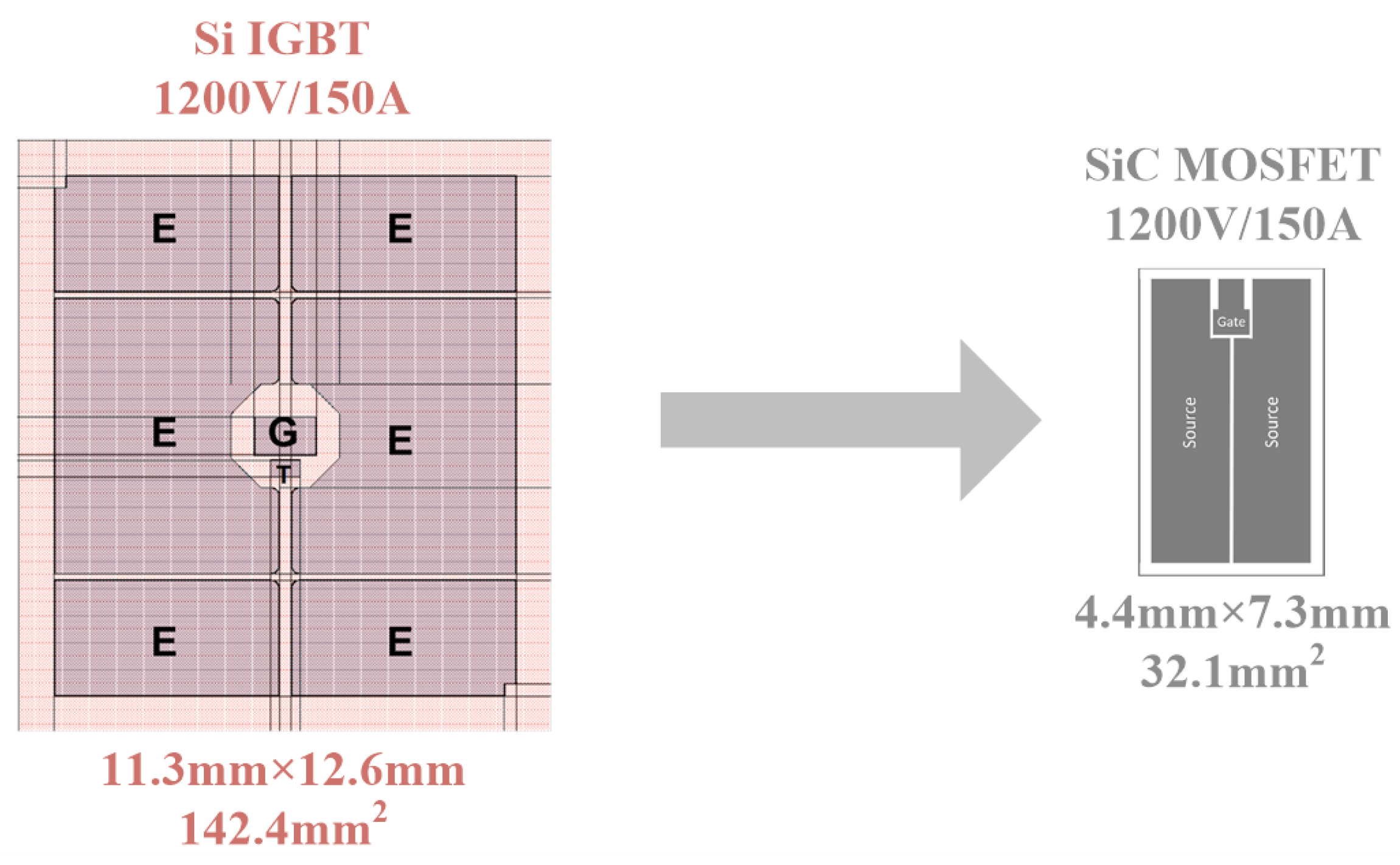
Figure 1. Size comparison of the Si IGBT (Infineon IGC142T120T8RH) and SiC MOSFET (CREE CPM3-1200-0013A) for the same rating [12].
Applsci 15 10869 g001
Figure 2. Conventional packaging structure of SiC power module.
Applsci 15 10869 g002
Figure 3. Topologies of the three-phase SiC-MMC inverter and HBSM.
Applsci 15 10869 g003
Figure 4. Operating modes of HBSM.
Applsci 15 10869 g004
Figure 5. MMC arm current.
Applsci 15 10869 g005
Figure 6. Mechanical Structure and working principle of VC.
Applsci 15 10869 g006
Figure 7. Vapor chambers as a substitute for the copper baseplate in conventional packaging structures.
Applsci 15 10869 g007
Figure 8. The mechanical structure proposed in this paper.
Applsci 15 10869 g008
Figure 9. Mechanical structure of the proposed asymmetric power module and a conventional power module (control group).
Applsci 15 10869 g009
Figure 10. Cross-sectional view of the internal structure of the VC in this study.
Applsci 15 10869 g010
Figure 11. (A) 3D structure of the power modules with heatsinks in FEM simulation. (B) Left and (C) front view of the geometries.
Applsci 15 10869 g011
Figure 12. Schematic diagram of the MATLAB–Simulink model of MMC.
Applsci 15 10869 g012
Figure 13. One-day apparent power profile of the MMC inverter [16].
Applsci 15 10869 g013
Figure 14. Device currents of the MMC inverter at (a) Smax and (b) 0.5Smax.
Applsci 15 10869 g014
Figure 15. Average power loss of the dies in MMC at (A) Smax and (B) 0.5Smax.
Applsci 15 10869 g015
Figure 16. Temperature contours of the (A) conventional module and (B) VC-based module at Smax.
Applsci 15 10869 g016
Figure 17. Junction temperature of the dies at Smax.
Applsci 15 10869 g017
Figure 18. Thermal distribution of the lower side DBC of (A) conventional and (B) VC-based power module.
Applsci 15 10869 g018
Figure 19. Temperature contours of the (A) conventional module and (B) VC-based module at 0.5Smax.
Applsci 15 10869 g019
Figure 20. Junction temperature of the dies at 0.5Smax.
Applsci 15 10869 g020
Figure 21. TSL of the dies.
Applsci 15 10869 g021
Figure 22. AD of the hotspot solder joint.
Applsci 15 10869 g022
Table 1. Operating Modes of HBSM.
ModesS1S2ismusm
A01ism > 00
B00ism > 0uc
C00ism < 00
D10ism < 0uc
Table 2. Parameters of the VC.
ParametersValue
VC size60 mm × 40 mm × 5 mm
Thickness of the copper shell1 mm
Thickness of the wick0.5 mm
Height of the vapor core2 mm
Working fluidWater
Working fluid filling weight1.5 g
Vacuum degree9.31 Pa (9.19 × 10⁻⁵ atm)
Table 3. Power Module Package Material Properties.
SheetMaterialsThickness
mm
Ther. Conduct
W/m·K
Spec. Heat
J/kg·K
MOSFETSiC0.175490690
DiodeSiC0.11490690
Chip solderPb40Sn600.132.7150
Top copperCopper0.3400385
CeramicAl2O30.6352430
Bottom CopperCopper0.3400385
DBC solderPb40Sn600.332.7150
BaseplateCopper3400385
TIMThermal grease0.151000
Table 4. Parameters of MMC Simulation Model.
SymbolMeaningValue
SNSystem rated apparent power0.83 MVA
PSystem active power0.75 MW
UdcDC-link voltage3 kV
UmAmplitude of ac side phase voltage1.35 kV
NNumber of SMs5
LArm inductor5 mH
RLLoad resistor2.965 Ω
LLLoad inductor4.58 mH
CSM capacitor4.7 mF
fsSwitching frequency1 k Hz
fFundamental frequency50 Hz
mModulation index0.9
Table 5. Measured Power Loss Coefficients for the SiC Schottky Diode.
Parameters U c o n d @ T r e f [V] r c o n d @ T r e f [Ω] K 3 [1] K 4 [1]
V a l u e s 0.94289 × 10⁻³−1.39 × 10−38.85 × 10−5
Disclaimer/Publisher’s Note: The statements, opinions and data contained in all publications are solely those of the individual author(s) and contributor(s) and not of MDPI and/or the editor(s). MDPI and/or the editor(s) disclaim responsibility for any injury to people or property resulting from any ideas, methods, instructions or products referred to in the content.