Abstract
We developed a low-particle emission linear atmospheric plasma device for hydrophilizing silicon wafers, aiming to improve semiconductor manufacturing processes. The device generates a stable plasma curtain using argon or helium gas under specific frequency and power conditions, enabling large-area surface treatment without causing damage. Experimental results demonstrated uniform hydrophilization, characterized by a substantial reduction in water contact angle and minimal particle emission, outperforming conventional jet-type plasma systems. TOF-SIMS analysis confirmed the absence of metal contamination, validating the device’s cleanliness. This technology offers a promising alternative to wet chemical treatments, contributing to environmentally friendly and efficient wafer bonding processes.
1. Introduction
Atmospheric plasma, which can be operated in open systems without the need for vacuum pumps or exhaust equipment, enables high-density and continuous treatment of reactive species. This characteristic has led to its application across various industrial fields, including semiconductor processing [1,2,3], decomposition of hazardous gases [4], detoxification of harmful substances [5], and elemental analysis. Furthermore, advancements in plasma temperature control technologies have expanded its potential use in medical devices and sterilization processes.
Semiconductor devices are essential to modern society, particularly integrated circuits, which are indispensable in communication, computing, and energy management. As global data traffic continues to increase annually, concerns regarding rising energy consumption and greenhouse gas emissions have intensified [6]. Enhancing the performance of semiconductor devices is considered one of the key solutions to these challenges. In semiconductor manufacturing, plasma processes play a crucial role in pattern formation via etching, dielectric film deposition through plasma Chemical Vapor Deposition, and wafer bonding via hydrophilization and contaminant removal. Historically, performance improvements have been achieved primarily through advancements in processing technologies for single-material systems such as silicon. However, the limitations of such approaches have become increasingly apparent [7]. Recent research has focused on photonic devices, which offer ultra-low power consumption and ultra-wide bandwidth capabilities [8,9,10]. In developing these devices, heterogeneous integration of silicon with III–V compound semiconductors has been proposed, enabling the realization of high-performance optical communication devices [11,12]. Heterogeneous integration refers to the fabrication of integrated circuits by optimally combining multiple semiconductor materials with distinct properties, thereby achieving device performance unattainable with single-material systems. This approach is especially important for optical communication applications.
Hydrophilic bonding has been proposed for joining dissimilar semiconductor materials. Traditionally, wet chemical treatments using oxidizing agents have been employed, but these require waste liquid treatment facilities and high-temperature annealing, prompting the need for simpler methods [13,14]. Recently, dry bonding techniques using low-pressure plasma in vacuum chambers have gained attention [15]. However, these methods involve complex processes and pose challenges for productivity [16,17,18,19,20]. Consequently, efforts have been made to simplify bonding processes by utilizing atmospheric plasma for hydrophilization [17,21].
Jet-type atmospheric plasma devices are commonly used, but they suffer from issues such as particle contamination due to electrode erosion, which can degrade cleanroom environments and device performance. Additionally, their narrow treatment width limits productivity [22]. To address these challenges, we have developed a novel linear-type plasma device with reduced particle generation. This device overcomes the limitations of conventional atmospheric plasma systems and enables inline integration with other bonding processes.
In this study, we describe the newly developed a low-particle emission linear plasma generation device and present experimental results evaluating its performance. Specifically, we report on the particle content within the plasma and the effectiveness of hydrophilization. The objective of this research is to propose a new plasma treatment method using atmospheric plasma that can be integrated inline with other bonding processes, and to develop and evaluate the performance of the corresponding device. This approach aims to achieve both effective hydrophilization of silicon wafers and suppression of particle contamination, thereby enhancing the efficiency of high-performance semiconductor device manufacturing.
2. Materials and Methods
2.1. Fabrication of the Linear Plasma Device
Traditionally, large-area plasma treatment has been conducted using dielectric barrier discharge (DBD) systems, which perform direct treatment by placing the target material inside the device and activating the surface via direct discharge [23]. However, for delicate materials such as silicon wafers, there is a risk of damage from discharge, necessitating the development of remote treatment technologies that enable large-area processing while avoiding discharge-induced damage.
To address this issue, a new large-area remote plasma treatment device was designed and fabricated based on the following principles. As shown in Figure 1, plasma was generated between copper and aluminum electrodes by flowing plasma-generating gas and applying alternating voltage, resulting in capacitively coupled plasma. The plasma is sustained by secondary electrons emitted when ions accelerated by the electric field collide with the electrodes.
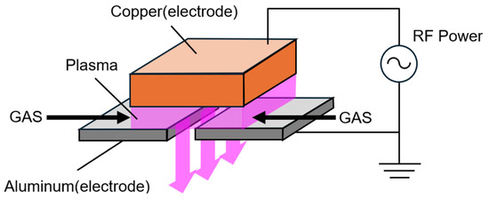
Figure 1.
Method for generating large-area remote plasma.
To ensure stable atmospheric plasma generation and minimize electrode damage, high-frequency power supplies of 13.56 MHz and 27.12 MHz were employed. At frequencies above 1 MHz, ions cannot follow the rapid changes in the electric field and become trapped in the discharge space, reducing collisions with electrodes. Consequently, plasma is maintained through ionization of gas molecules via electron collisions [24].
A slit measuring 349 mm × 1 mm was installed at the bottom of the device to emit plasma in a curtain-like fashion, enabling large-area remote treatment. As shown in Figure 2, the linear plasma device is enclosed in an aluminum housing with only the slit section machined. The housing is grounded, and plasma is generated between the internal copper electrodes. The hollow copper electrodes are cooled by circulating a coolant to suppress heat buildup. Additionally, a mechanism for uniform gas flow distribution is incorporated within the housing.
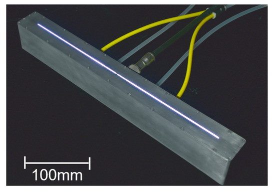
Figure 2.
Developed linear plasma device.
The housing dimensions are 53 mm in height, 405 mm in width, and 40 mm in depth. Symmetrical gas and coolant inlets are positioned on both sides, and a coaxial cable adapter is located at the center. Plasma generation was successfully achieved by flowing argon or helium gas and applying high-frequency voltage at 13.56 MHz or 27.12 MHz. To ensure optimal power transfer during plasma generation, impedance matching was performed using a matching box, effectively eliminating reflected power. The curtain-shaped plasma emitted from the slit allows for single-pass treatment of 12-inch wafers.
Optical emission spectroscopy of the plasma was performed by collecting the emitted light through an optical fiber P-100-1-SR (Ocean Insight Inc., Orlando, FL, USA) positioned 200 mm from the edge of the irradiation slit and 30 mm above the slit plane. The light was then introduced into a multichannel spectrometer MAYA2000PRO HC-1 (Ocean Optics Inc., Orlando, FL, USA) to obtain the emission spectra.
The plasma temperature was measured using an optical fiber thermometer FTX-300-LUX+ (OSENSA Innovations Corp., Burnaby, BC, Canada) positioned 200 mm from the edge of the irradiation slit. To match the conditions of the Si wafer, the temperature was recorded after 1 min of plasma exposure at a location 1 mm above the slit plane.
2.2. Performance Evaluation and Comparative Experiments
To evaluate hydrophilization performance, water contact angle measurements were conducted using the B100 instrument (Asumi Giken Co., Ltd, Tokyo, Japan). While additional evaluation methods such as surface free energy analysis using diiodomethane [25] and functional group analysis via X-ray Photoelectron Spectroscopy [26] were considered, this study focused on basic validation using water contact angle measurements. Contact angle measurements were conducted using a droplet volume of 1 μL at a room temperature of 20 °C.
The method for measuring the number of particles emitted from the plasma device is illustrated in Figure 3. The device was sealed in a clean bag 1-3254-07 (AS ONE Corp., Osaka, Japan), and plasma was generated. The number of airborne particles inside the bag was measured using a particle counter KC-01E (RION Co., Ltd., Tokyo, Japan). In this setup, the plasma emitted from the device was directly and continuously measured in real time. Argon gas was used as the plasma-generating gas, and particles larger than 0.1 μm were removed using a filter FUFL-915-6.35-0.1 (Fujikin Inc., Osaka, Japan). Measurements were repeated five times, and the average values were used for analysis. The detailed setup is provided in Supplementary Material Figure S1. Gas was collected at a position approximately 40 mm from the slit.
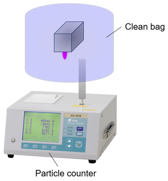
Figure 3.
Method for measuring the number of particles emitted from the plasma device.
For comparison, particle emissions from a conventional jet-type plasma device was also measured. This device is 85 mm in length and weighs 160 g, with a 1.5 mm gap between the high-voltage and ground electrodes. Plasma is generated by flowing gas and applying 16 W at 16 kHz, which is emitted through a 1 mm diameter nozzle [5,22]. A schematic diagram of a conventional jet-type plasma device is presented in Figure 4. The device operates by generating plasma through high-voltage discharge between electrodes, which is subsequently expelled from the nozzle outlet.
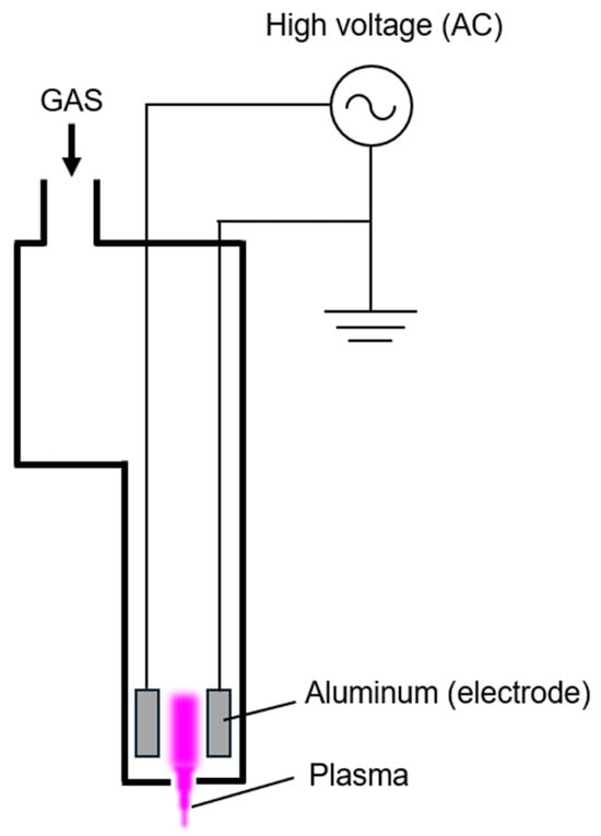
Figure 4.
Schematic a conventional jet-type plasma device.
Additionally, surface analysis of adsorbed substances after treatment with both the linear and jet-type plasma devices was conducted using Time-of-Flight Secondary Ion Mass Spectrometry (TOF-SIMS, ION-TOF GmbH, Münster, Germany). Bi3+ ions were used as the primary ion species. The measurements were performed with a primary acceleration voltage of 30 kV, a beam diameter of approximately 3–4 μm, and an incident current of 0.2 pA per 100 μs. An electron flood gun was also employed for charge neutralization.
3. Results
3.1. Conditions for Stable Plasma Generation in the Linear Plasma Device
To determine the operational conditions for stable plasma generation using the developed linear plasma device, the relationship between gas flow rate and power output was investigated for both argon and helium gases. Figure 5 illustrates the range of conditions under which stable argon plasma was generated at a frequency of 13.56 MHz. Stable plasma was observed within a gas flow rate range of 5–40 L/min and a power output range of 40–80 W. Figure 6 shows the conditions for stable helium plasma generation, which occurred within a flow rate range of 10–40 L/min and a power output range of 40–70 W. Compared to argon, helium exhibited a narrower range of stable conditions, particularly at higher flow rates where localized arc discharges were more likely to occur. Figure 7 and Figure 8 present the emission spectrum of plasmas generated using argon and helium gases, respectively, each supplied at a flow rate of 30 L/min and an output power of 60 W. Under these conditions, the plasma gas temperature measured at a position 1 mm from the nozzle was 58.9 °C for argon and 30.3 °C for helium.
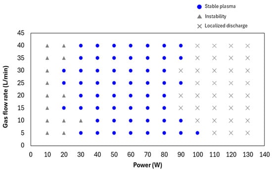
Figure 5.
Conditions for stable argon plasma generation at a frequency of 13.56 MHz.
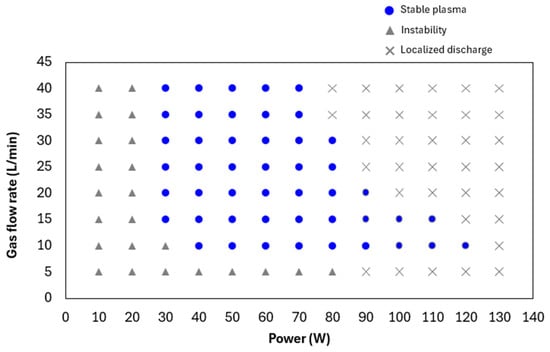
Figure 6.
Range of conditions for stable plasma generation using helium gas.
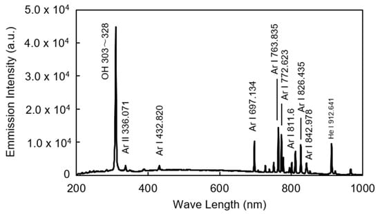
Figure 7.
Emission spectrum of argon plasma in the range of 200–1000 nm (Ar 30 L/min, Power 60 W).
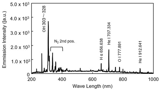
Figure 8.
Emission spectrum of helium plasma in the range of 200–1000 nm (He 30 L/min, Power 60 W).
3.2. Evaluation of Hydrophilization Effect
To assess the uniformity of the plasma treatment effect, argon plasma was linearly irradiated onto silicon wafers, and hydrophilization was evaluated via contact angle measurements. Similar approaches to evaluating spatial uniformity using plasma microjet arrays have been reported [27,28]. Figure 9 outlines the experimental setup using the linear plasma device. The plasma was generated using a 13.56 MHz power supply at 60 W, with argon gas supplied at a flow rate of 30 L/min. The plasma was irradiated onto a 2-inch silicon wafer at a distance of 1 mm and a scanning speed of 4 mm/sec. Prior to treatment, the wafers were immersed in buffered hydrofluoric acid (BHF; NH4HF2 21%, NH4F 21%, H2O 58%) for 3 min, followed by immersion in pure water for an additional 3 min to perform cleaning. Subsequently, nitrogen gas was blown over the wafer surfaces to remove residual water droplets and ensure complete drying. To verify the uniformity of treatment across the width, five silicon wafers were arranged at 80 mm intervals, and contact angles were measured at five points per wafer. Figure 10 presents the results. The average contact angle of the cleaned wafers was 72.5°, which decreased to 13.1° after plasma treatment. The standard deviation across the width was 3.0°, indicating a high level of uniformity in hydrophilization.
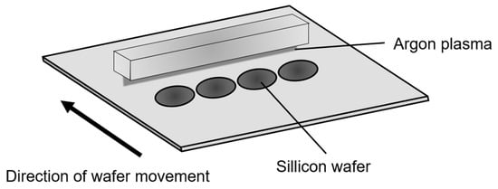
Figure 9.
Experimental setup for hydrophilization of silicon using the linear plasma device.
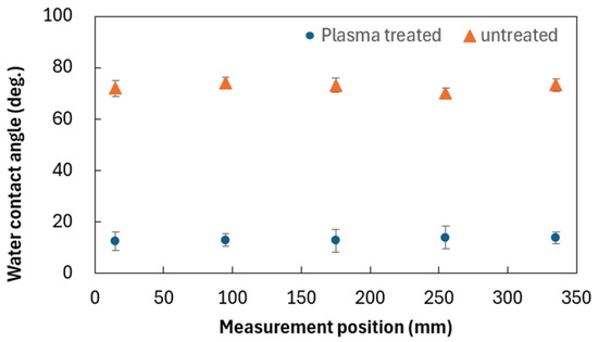
Figure 10.
Hydrophilization results of silicon using the linear plasma device.
3.3. Evaluation of Particle Suppression Performance
The number of particles emitted from the linear plasma device was measured and compared with that from a conventional jet-type plasma device. The linear device operated at 27.12 MHz with an argon flow rate of 30 L/min and a power output of 165 W. The jet-type device operated at 16 kHz with an argon flow rate of 2 L/min and a voltage of 16 W. Figure 11 shows the particle count results across various size ranges: 0.3–0.5 μm, 0.5–1 μm, 1–2 μm, 2–5 μm, and >5 μm. Jet-type plasma device generated 5.5 × 10⁵, 1.0 × 10⁵, 2.3 × 10⁴, 1.0 × 10³, and 8.0 particles/L, respectively, in these size ranges. In contrast, the linear plasma device produced fewer than 1.0 particles/L in all size categories, demonstrating its capability as a clean plasma source. When converted to particle count per unit power, the jet-type plasma device yielded 3.4 × 10⁴, 6.3 × 10³, 1.4 × 10³, 6.3 × 10, and 5.0 × 10⁻¹ particles/L·W, respectively.
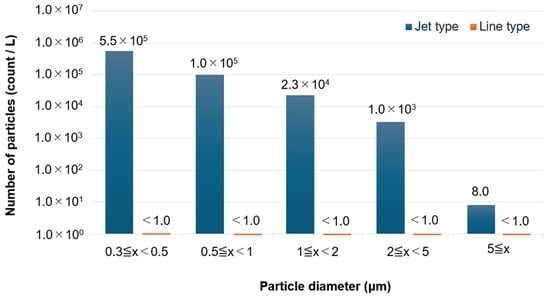
Figure 11.
Particle emissions from the linear plasma device.
Figure 12 presents TOF-SIMS analysis results of silicon wafers treated by both devices. Aluminum was detected on the surface treated by the jet-type device, likely originating from electrode erosion. No significant aluminum peaks were observed on the surface treated by the linear device, indicating effective suppression of metal contamination.
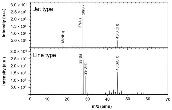
Figure 12.
Chemical composition of silicon surfaces treated by jet-type and linear plasma devices.
4. Discussion
In recent years, various surface activation techniques such as wet chemical treatments, UV irradiation, and thermal annealing have been explored for wafer bonding. However, these methods often involve complex processes, environmental burdens, or limitations in scalability. Plasma treatment, particularly atmospheric plasma, offers a unique combination of advantages: it enables damage-free, large-area processing under ambient conditions, minimizes chemical waste, and allows inline integration with existing semiconductor manufacturing workflows. These features make plasma an especially attractive solution for hydrophilization in heterogeneous wafer bonding applications. Compared to conventional wet chemical or UV-based treatments, the developed atmospheric plasma device provides a cleaner and more controllable surface modification process. Its ability to operate under ambient pressure without introducing additional contaminants or requiring post-treatment annealing highlights its practical superiority. Furthermore, the linear configuration enables uniform treatment over large wafer areas, which is challenging to achieve with other methods.
In this study, a linear-type atmospheric plasma device capable of emitting plasma in a curtain-like fashion was developed, and the conditions for stable plasma generation at a frequency of 13.56 MHz were investigated. For argon gas, stable plasma was achieved within a flow rate range of 5–40 L/min and a power range of 40–80 W. For helium gas, the stable range was narrower, with flow rates of 10–40 L/min and power outputs of 40–70 W. Although helium’s higher thermal conductivity suggests more diffuse discharge, the experimental results contradicted this expectation [29,30]. Helium also has higher viscosity [31,32], which should suppress turbulent discharge [33,34]. In practice, stable plasma was generated under high-power conditions with helium. However, instability was observed at both low and high flow rates, likely due to density fluctuations in the gas stream. These fluctuations may cause instability under gravitational or acceleration fields [35]. Additionally, low flow rates may allow ambient air to mix into the plasma, further destabilizing it. Therefore, maintaining uniform flow conditions is essential for achieving stable plasma generation with helium, similar to argon. The results of optical emission spectroscopy of the plasma revealed spectral lines attributed to OH and N2, indicating that the plasma interacts with atmospheric gases. Furthermore, based on the plasma gas temperature measurements, it is inferred that the thermal impact on the Si wafer is minimal.
In the hydrophilization experiments using silicon wafers, the contact angle was uniformly reduced across the entire slit width, with an average value of 13.1°. This value is comparable to those reported in previous studies [36,37], suggesting that the developed device could serve as a promising alternative. Further enhancement of hydrophilicity may be achievable by using oxygen gas or optimizing other parameters. It has also been confirmed separately that increasing the treatment time or the number of treatment cycles enhances the hydrophilic effect. For instance, when a 12-inch wafer was irradiated for 152 s, the contact angle improved to 4.1°.
Particle emission measurements revealed that the developed linear plasma device did not emit detectable particles larger than 0.3 μm, indicating its suitability for cleanroom environments in semiconductor manufacturing. TOF-SIMS analysis showed no aluminum contamination on the silicon wafer surface treated with the linear device, whereas aluminum was detected on wafers treated with the jet-type device. This suggests that the use of high-frequency power at 27.12 MHz reduces ion collisions with electrodes, thereby minimizing electrode erosion and particle generation.
While the device successfully generated stable atmospheric plasma across a 349 mm width and achieved uniform hydrophilization of silicon wafers, further improvements are needed for integration into semiconductor manufacturing processes. Specifically, the hydrophilization effect must be enhanced, as the contact angle achieved is higher than that of conventional low-pressure plasma treatments. Future work will focus on optimizing gas types, frequencies, and power levels to advance atmospheric plasma processing technologies.
5. Conclusions
In this study, we developed a novel low-particle emission linear atmospheric plasma device capable of uniformly hydrophilizing silicon wafers over a wide area. The device generates a stable plasma curtain using argon or helium gas under high-frequency conditions, enabling remote surface treatment. Experimental results showed that the water contact angle on silicon surfaces decreased uniformly across the entire treatment width, with an average value of 13.1°. This value is comparable to those reported in previous technologies, and further improvements in hydrophilization performance are expected through optimization of gas types and processing conditions.
Moreover, particle emission measurements confirmed that the device emitted virtually no particles larger than 0.3 μm, demonstrating a significantly cleaner processing environment compared to conventional jet-type plasma devices. TOF-SIMS analysis also revealed no metal contamination on the treated silicon surfaces, validating the cleanliness of the device. These results suggest that the developed system offers a promising, environmentally friendly alternative to wet chemical treatments and is well-suited for inline processing.
Future work will focus on further enhancing hydrophilization performance and adapting the system for semiconductor manufacturing applications by investigating detailed processing parameters such as gas composition, frequency, and power. Previous studies have indicated that maintaining hydrophilicity over time on plasma-treated Si/SiO2 surfaces remains a challenge [5]. Furthermore, to improve cost-efficiency in large-scale manufacturing, it is essential to address issues such as reducing gas consumption, which is currently relatively high in the present system. The outcomes of this research lay the foundation for next-generation atmospheric plasma technologies that combine high cleanliness and processing efficiency, contributing to the advancement of semiconductor device fabrication.
Supplementary Materials
The following supporting information can be downloaded at: https://www.mdpi.com/article/10.3390/app151910349/s1, Figure S1: The setup used for particle counting is shown.
Author Contributions
Conceptualization, S.Y., A.O. and N.N.; methodology, S.Y., K.H. and A.O.; investigation, S.Y., K.H. and J.F.; writing—original draft preparation, S.Y.; writing—review and editing, T.O. and A.Y.; project administration, A.O. and N.N. All authors have read and agreed to the published version of the manuscript.
Funding
This research received no external funding.
Institutional Review Board Statement
Not applicable.
Informed Consent Statement
Not applicable.
Data Availability Statement
The raw data supporting the conclusions of this article will be made available by the authors on request.
Acknowledgments
A part of this research was supported by JSPS KAKENHI Grant-in-Aid for Scientific Research (S) 22H04973.
Conflicts of Interest
The authors have no conflicts of interest to declare.
References
- Abe, H.; Yoneda, M.; Fujiwara, N. Developments of Plasma Etching Technology for Fabricating Semiconductor Devices. Jpn. J. Appl. Phys. 2008, 47, 1435–1455. [Google Scholar] [CrossRef]
- Chiappim, W.; Neto, B.B.; Shiotani, M.; Karnopp, J.; Gonçalves, L.; Chaves, J.P.; da Silva Sobrinho, A.; Leitão, J.P.; Fraga, M.; Pessoa, R. Plasma-Assisted Nanofabrication: The Potential and Challenges in Atomic Layer Deposition and Etching. Nanomaterials 2022, 12, 3497. [Google Scholar] [CrossRef]
- Ryu, S.H.; Hwang, I.; Jeon, D.; Lee, S.K.; Chung, T.-M.; Han, J.H.; Chae, S.; Baek, I.-H.; Kim, S.K. Plasma-enhanced atomic layer deposition of indium-free ZnSnOₓ thin films for thin-film transistors. Appl. Surf. Sci. 2025, 680, 161320. [Google Scholar] [CrossRef]
- Tamura, T.; Kaburaki, Y.; Sasaki, R.; Miyahara, H.; Okino, A. Direct decomposition of anesthetic gas exhaust using atmospheric pressure multigas inductively coupled plasma. IEEE Trans. Plasma Sci. 2011, 39, 1684–1688. [Google Scholar] [CrossRef]
- Takamatsu, T.; Miyahara, H.; Azuma, T.; Okino, A. Investigation of reactive species using various gas plasmas. J. Toxicol. Sci. 2014, 39, 281–290. [Google Scholar] [CrossRef] [PubMed]
- Andrae, A.S.G.; Edler, T. On Global Electricity Usage of Communication Technology: Trends to 2030. Challenges 2015, 6, 117–157. [Google Scholar] [CrossRef]
- Johnsson, L.; Netzer, G. The impact of Moore’s Law and loss of Dennard scaling: Are DSP SoCs an energy efficient alternative to x86 SoCs? J. Phys. Conf. Ser. 2016, 762, 012022. [Google Scholar] [CrossRef]
- Moody, G.; Islam, M.S. Materials for ultra-efficient, high-speed optoelectronics. MRS Bull. 2022, 47, 475–484. [Google Scholar] [CrossRef]
- Wang, Z.; Li, X.; Ji, J.; Sun, Z.; Sun, J.; Fang, B.; Lu, J.; Li, S.; Ma, X.; Chen, X.; et al. Fast-speed and low-power-consumption optical phased array based on lithium niobate waveguides. Nanophotonics 2024, 13, 13. [Google Scholar] [CrossRef]
- Rani, A.; Dewra, S. Semiconductor Optical Amplifiers in Optical Communication Systems—Review. Int. J. Eng. Res. Technol. 2013, 2, 1006–1010. [Google Scholar]
- Duan, G.H.; Jany, C.; Le Liepvre, A.; Accard, A.; Lamponi, M.; Make, D.; Kaspar, P.; Levaufre, G.; Girard, N.; Lelarge, F.; et al. Hybrid III-V on Silicon Lasers for Photonic Integrated Circuits on Silicon. IEEE J. Sel. Top. Quantum Electron. 2015, 21, 379–391. [Google Scholar]
- Fang, W.; Takahashi, N.; Ohiso, Y.; Amemiya, T.; Nishiyama, N. Reduced Thermal Resistance of Membrane Fabry-Perot Laser Bonded on Si Through Room-Temperature, Surface-Activated Bonding Assisted by a-Si Nano-Film. IEEE J. Quantum Electron. 2022, 58, 2000208. [Google Scholar] [CrossRef]
- Maszara, W.P.; Pronko, P.P.; McCormick, A.W. Epi-less bond-and-etch-back silicon-on-insulator by MeV ion implantation. Appl. Phys. Lett. 1991, 58, 2779–2781. [Google Scholar] [CrossRef]
- Takagi, H. Room-temperature wafer bonding. Surf. Sci. 2005, 26, 82–87. [Google Scholar] [CrossRef][Green Version]
- Qin, Y.; Howlader, M.M.R.; Deen, M.J. Low-Temperature Bonding for Silicon-Based Micro-Optical Systems. Photonics 2015, 2, 1164–1201. [Google Scholar] [CrossRef]
- Encinas, N.; Dillingham, R.G.; Oakley, B.R.; Abenojar, J.; Martínez, M.A.; Pantoja, M. Atmospheric Pressure Plasma Hydrophilic Modification of a Silicone Surface. J. Adhes. 2012, 88, 321–336. [Google Scholar] [CrossRef]
- Suni, T.; Henttinen, K.; Suni, I.; Mäkinen, J. Effects of Plasma Activation on Hydrophilic Bonding of Si and SiO2. J. Electrochem. Soc. 2002, 149, G348–G351. [Google Scholar] [CrossRef]
- Ma, X.; Chen, C.; Liu, W.; Liu, X.; Du, X.; Song, Z.; Lin, C. Study of the Ge Wafer Surface Hydrophilicity after Low-Temperature Plasma Activation. J. Electrochem. Soc. 2009, 156, H307–H311. [Google Scholar] [CrossRef]
- Esser, R.H.; Hobart, K.D.; Kub, F.J. Improved Low-Temperature Si–Si Hydrophilic Wafer Bonding. J. Electrochem. Soc. 2003, 150, G228–G232. [Google Scholar] [CrossRef]
- Tong, Q.-Y.; Gan, Q.; Hudson, G.; Fountain, G.; Enquist, P. Low temperature InP/Si wafer bonding. Appl. Phys. Lett. 2004, 84, 732–734. [Google Scholar] [CrossRef]
- Lee, Y.; You, Y.; Cho, C.; Kim, S.; Lee, J.; Kim, M.; Lee, H.; You, Y.; Kim, K.; You, S. Comprehensive assessments in bonding energy of plasma assisted Si–SiO2 direct wafer bonding after low temperature rapid thermal annealing. Micromachines 2022, 13, 1856. [Google Scholar] [CrossRef]
- Takamatsu, T.; Hirai, H.; Sasaki, R.; Miyahara, H.; Okino, A. Surface Hydrophilization of Polyimide Films Using Atmospheric Damage-Free Multigas Plasma Jet Source. IEEE Trans. Plasma Sci. 2013, 41, 119–125. [Google Scholar] [CrossRef]
- Wagner, H.-E.; Brandenburg, R.; Kozlov, K.V.; Sonnenfeld, A.; Michel, P.; Behnke, J.F. The barrier discharge: Basic properties and applications to surface treatment. Vacuum 2003, 71, 417–436. [Google Scholar] [CrossRef]
- Yin, G.Q.; Wang, J.J.; Yuan, Q.H. The Discharge Characteristics of Capacitively Coupled Ar Plasma as the Change of Pressure. Plasma Phys. Rep. 2023, 49, 802–807. [Google Scholar] [CrossRef]
- Chibowski, E.; Jurak, M. Comparison of contact angle hysteresis of different probe liquids on the same solid surface. Colloid Polym. Sci. 2013, 291, 391–399. [Google Scholar] [CrossRef] [PubMed]
- Head, A.R.; Schnadt, J. UHV and Ambient Pressure XPS: Potentials for Mg, MgO, and Mg(OH)2 Surface Analysis. JOM 2016, 68, 3070–3077. [Google Scholar] [CrossRef]
- Yang, J.; Xia, L.; Zhou, S.; Liao, L.; Wang, Z.; Wen, L.; Yan, K.C.; Wang, H.; Chu, J. Study of uniformity of atmospheric pressure plasma microjet array for maskless parallel micropatterned etching. Plasma Process. Polym. 2022, 19, e2100167. [Google Scholar] [CrossRef]
- Suzuki, H.; Koma, H.; Ogasawara, T.; Koike, Y.; Toyoda, H. Spatial uniformity evaluation of atmospheric-pressure microwave line plasma for wide-area surface treatment. Plasma Fusion Res. 2021, 16, 1406046. [Google Scholar] [CrossRef]
- Pateyron, B.; Elchinger, M.-F.; Delluc, G.; Fauchais, P. Thermodynamic and transport properties of Ar-H2 and Ar-He plasma gases used for spraying at atmospheric pressure. Plasma Chem. Plasma Process. 1992, 12, 421–448. [Google Scholar] [CrossRef]
- Hori, M. Radical-controlled plasma processes. Rev. Mod. Plasma Phys. 2022, 6, 36. [Google Scholar] [CrossRef]
- May, E.F.; Berg, R.F.; Moldover, M.R. Reference Viscosities of H2, CH4, Ar, and Xe at Low Densities. Int. J. Thermophys. 2007, 28, 1085–1110. [Google Scholar] [CrossRef]
- Golovicher, L.E.; Kolenchits, O.A.; Nesterov, N.A. Dynamic viscosity of gases over a wide range of temperatures. J. Eng. Phys. Thermophys. 1989, 56, 689–694. [Google Scholar] [CrossRef]
- Yoshida, H.; Takei, Y.; Arai, K. Equations for Calculating the Gas Flow Rate through a Cylindrical Tube in Various Flow Regimes. Vac. Surf. Sci. 2020, 63, 304–310. [Google Scholar] [CrossRef]
- Senda, Y. Theoretical Analysis of Vacuum Evacuation in Viscous Flow and Its Applications. SEI Tech. Rev. 2010, 176, 1–7. [Google Scholar]
- Villarreal-Medina, R.; Murphy, A.B.; Méndez, P.F.; Ramírez-Argáez, M.A. Heat Transfer Mechanisms in Arcs of Various Gases at Atmospheric Pressure. Plasma Chem. Plasma Process. 2023, 43, 787–803. [Google Scholar] [CrossRef]
- Abdilla, J.; See, G.H. Chip-to-Wafer Hybrid Bonding Development for High Volume Manufacturing. IMAPSource Proc. 2023. [Google Scholar] [CrossRef]
- Alam, A.U.; Howlader, M.M.R.; Deen, M.J. The effects of oxygen plasma and humidity on surface roughness, water contact angle and hardness of silicon, silicon dioxide and glass. J. Micromech. Microeng. 2014, 24, 035010. [Google Scholar] [CrossRef]
Disclaimer/Publisher’s Note: The statements, opinions and data contained in all publications are solely those of the individual author(s) and contributor(s) and not of MDPI and/or the editor(s). MDPI and/or the editor(s) disclaim responsibility for any injury to people or property resulting from any ideas, methods, instructions or products referred to in the content. |
© 2025 by the authors. Licensee MDPI, Basel, Switzerland. This article is an open access article distributed under the terms and conditions of the Creative Commons Attribution (CC BY) license (https://creativecommons.org/licenses/by/4.0/).