1. Introduction
As the miniaturization of transistors approaches its physical and economic boundaries, the semiconductor industry is increasingly turning to three-dimensional integrated circuits (3DICs) as a viable path forward for enhancing device performance and transistor density [
1]. Unlike conventional two-dimensional integrated circuits (2DICs), where signal routing is confined to a single plane, 3DICs employ vertical stacking of silicon (Si) dies. These stacked dies are interconnected using Through-Silicon Vias (TSVs), which enable high-density vertical signal transmission and significantly reduce interconnect length [
2,
3,
4]. The integration of TSVs is typically achieved through advanced bonding techniques such as hybrid bonding or oxide bonding, which offer improved alignment accuracy and electrical performance [
5].
The adoption of 3DIC technology with TSVs offers several compelling advantages over traditional packaging methods. These include reduced power consumption, smaller form factors, and increased bandwidth, all of which are critical for meeting the demands of modern high-performance computing and mobile applications [
6]. Copper (Cu) is commonly used as the TSV filling material due to its superior electrical and thermal conductivity, which facilitates efficient signal transmission and heat dissipation [
7].
However, the integration of Cu-filled TSVs introduces significant reliability challenges. One of the primary concerns arises from the large mismatch in the coefficient of thermal expansion (CTE) between Cu and Si. During thermal cycling, this mismatch generates substantial mechanical stress at the Cu–Si interface, which can lead to structural failures such as delamination, cracking, and void formation [
8]. To mitigate these risks, a keep-out zone (KOZ) is typically defined around each TSV, within which no active devices are placed. This design rule helps prevent stress-induced degradation of device performance but also reduces the effective area available for circuit integration.
To address these challenges, researchers have proposed various strategies aimed at minimizing the KOZ and improving thermal management. These include the use of alternative TSV materials with better CTE compatibility, innovative TSV geometries that distribute stress more evenly, and optimized TSV array layouts that reduce thermal coupling effects [
9,
10,
11,
12,
13]. In addition, simulation-based approaches, particularly those utilizing finite element analysis (FEA), have been widely employed to model the thermal and mechanical behavior of TSVs under different operating conditions. These simulations typically focus on the final device structure, providing valuable insights into the stress distribution and thermal gradients resulting from CTE mismatch [
14,
15,
16].
Recent advancements in 3D integrated circuits (3DICs) have underscored the critical importance of understanding their thermo-mechanical reliability, particularly concerning through-silicon vias (TSVs). Extensive research has been conducted using both experimental and simulation-based approaches to characterize these behaviors. For example, Chen et al. [
17] utilized a combination of finite element modeling and thermal cycling experiments to elucidate the intricate stress evolution mechanisms within copper-filled TSVs. Similarly, Jung et al. [
18] developed a comprehensive, full-chip stress-aware analysis framework that leverages linear superposition and reliability metrics to optimize TSV layouts for enhanced performance. Furthermore, Altmann et al. [
19] highlighted the crucial need for sophisticated failure analysis techniques capable of capturing stress accumulation that occurs during intermediate processing stages.
Despite significant advancements in the field, a critical gap persists in the current body of research: most investigations focus predominantly on the final device structure, often overlooking the cumulative impact of stresses and temperature variations introduced during intermediate manufacturing steps. This omission limits the ability to identify root causes of reliability issues and hinders the development of robust design and fabrication strategies. To address this, our study introduces a novel process-aware simulation framework that captures the dynamic evolution of thermo-mechanical behavior throughout the entire 3D stacking process from initial fabrication to final device assembly. By adopting this comprehensive approach, we aim to provide a more accurate assessment of reliability risks and offer practical, data-driven guidance for optimizing TSV layouts, particularly in demanding high-performance sensor applications.
By modeling the progression of stress and temperature distributions throughout the fabrication flow, we aim to uncover the underlying mechanisms that contribute to reliability degradation. Our simulation framework incorporates realistic material properties, process parameters, and thermal loading conditions to accurately reflect the behavior of TSV-integrated structures.
In this study, the thermal and mechanical differences introduced at each fabrication process, such as TSV etching, CMP, annealing, and bonding, cumulatively affect stress evolution and device reliability. Our simulation framework captures these variations step-by-step to assess their impact on the mechanical integrity of 3DIC structures.
Additionally, we explore the impact of TSV pitch on both mechanical stress and thermal performance. By analyzing configurations with varying TSV spacing, we assess the extent of thermal stress interaction between adjacent TSVs and its implications for KOZ design. Our findings demonstrate that while closely spaced TSVs increase stress coupling and necessitate larger KOZs, they also enhance heat dissipation due to the high thermal conductivity of Cu. These insights provide a foundation for optimizing TSV design to balance reliability and thermal efficiency in future 3DIC systems.
2. Methods
Figure 1 and
Table 1 illustrate the process flow and device dimensions used in the 3D oxide-bonded stacking structure with TSV interconnects, as simulated in this study [
5]. The fabrication process is divided into five key steps, each involving specific thermal and mechanical conditions. In
Table 1, the parameters h1–h5 and w1–w4 represent the vertical and lateral dimensions of each layer in the 3D stacked structure, respectively. Specifically, h1–h5 correspond to the thicknesses of the silicon substrate, oxide layers, and redistribution layers, while w1–w4 define the lateral widths of the TSV, oxide trench, and metal interconnects. At every stage, the structure is subjected to its respective processing temperature, as detailed in
Table 2, and subsequently cooled to room temperature before proceeding to the next step. This thermal cycling is critical for accurately capturing the evolution of stress and temperature distributions throughout the process.
The first step involves the etching and formation of TSVs. Although sidewall roughness is typically introduced during the etching process, it is neglected in this simulation due to its negligible scale relative to the overall structure [
20]. In Step 2, the chemical mechanical planarization (CMP) process is performed to reveal the TSVs. The interaction between the polishing pad and the substrate is modeled by applying a frictional force at the interface, which contributes to the mechanical stress profile of the structure.
In Step 2, the chemical mechanical planarization (CMP) process is modeled by applying a frictional force at the pad–substrate interface. While specific values such as friction coefficient, pad pressure, and sliding speed are not explicitly defined in this study, the mechanical load is treated qualitatively to reflect typical CMP conditions. The simulation results indicate that thermal stress—arising from CTE mismatch—dominates the overall stress profile, and CMP-induced mechanical loads are considered secondary.
Step 3 focuses on the formation of the front-side redistribution layer (RDL), where aluminum (Al) is used as the interconnect material. Following the RDL patterning, an annealing process is applied to relieve thermal stress accumulated during metal deposition. In Step 4, two wafers are aligned and bonded using an oxide bonding technique [
5], which does not require any adhesive layers. This bonding method ensures strong mechanical integrity and electrical continuity between the stacked dies. Finally, Step 5 includes the TSV reveal process on the back side, followed by the formation of the back-side RDL using copper (Cu). A final annealing step is conducted to complete the oxide-bonded stacking process and stabilize the structure.
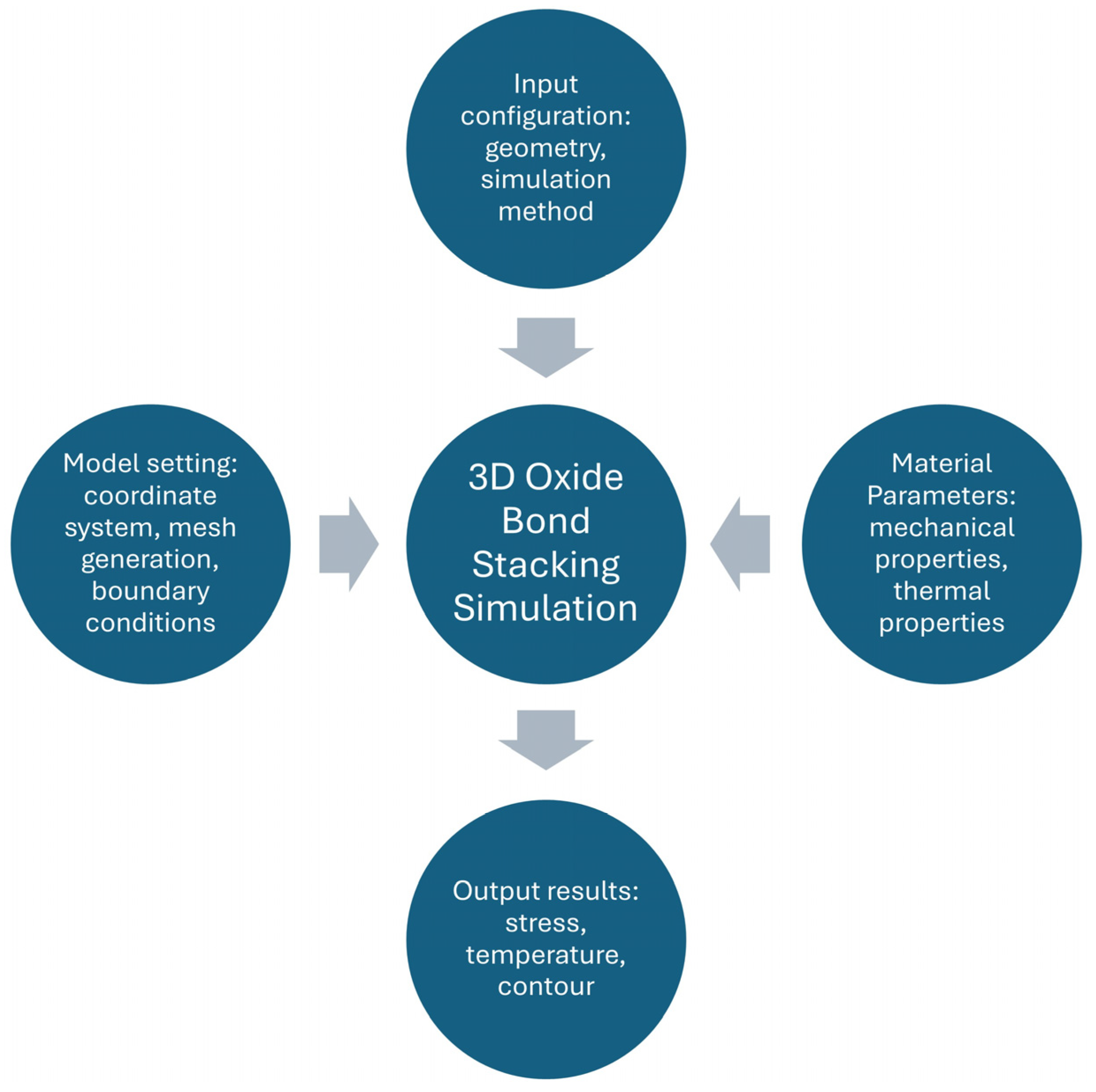
To analyze the thermo-mechanical behavior of the structure, two finite element analysis (FEA) approaches are employed: thermal-mechanical simulation and transient thermal simulation. FEA is a powerful numerical method widely used to model physical phenomena such as thermal stress, temperature gradients, and structural deformation. The overall simulation framework and methodology are depicted in
Figure 2 for reference.
All materials used in the simulation are assumed to be isotropic and linearly elastic, with their properties summarized in
Table 3 [
14]. Special attention is given to mesh generation, particularly at material interfaces, where stress concentrations are most likely to occur. Advanced meshing techniques are applied to ensure accuracy and convergence in these critical regions, as shown in
Figure 1. While early-stage thermo-mechanical modeling often simplifies simulations by assuming isotropic and linearly elastic material behavior, we acknowledge that copper (Cu), especially within TSV structures, can exhibit plastic deformation under significant thermal and mechanical loads. For this study, however, the simulated process conditions resulted in stress levels within the copper that remained below its typical yield strength. This observation justifies our use of an elastic approximation for the intended analysis.
To ensure consistency with prior simulation studies, the Young’s modulus of copper was set to 70 GPa, as reported in Pan et al. [
14]. This value, while lower than the commonly cited range of 110–130 GPa for room-temperature copper, reflects a modeling simplification frequently adopted in thermo-mechanical analyses of TSV structures. Using this parameter facilitates direct comparison of stress evolution trends and supports validation against established benchmarks.
It is important to acknowledge that the assumption of linear elasticity for copper (Cu) represents a simplification in our simulation model. While this assumption is justified by the fact that the simulated stress levels remained below the typical yield strength of Cu, it does not account for potential plastic deformation or creep effects that may arise under prolonged thermal cycling or elevated temperatures.
Nevertheless, we recognize that incorporating plasticity and anisotropic effects would undoubtedly enhance the model’s accuracy, particularly for long-term reliability assessments or under extreme thermal cycling conditions. Therefore, our future work will focus on integrating more advanced material models, including elasto-plastic and creep behavior, to capture these complex effects more comprehensively.
In the mechanical simulation model, the bottom surface of the silicon substrate is fixed to represent wafer handling during fabrication, while all other surfaces are traction-free to emulate unconstrained thermal expansion. At bonded and oxide interfaces, perfect adhesion is assumed, with no delamination or sliding, reflecting ideal bonding conditions typically achieved in oxide–oxide direct bonding processes. These boundary conditions are chosen to isolate the effects of thermal mismatch and material interfaces on stress evolution. While interface imperfections may influence local stress concentrations, their inclusion is deferred to future work focused on reliability under non-ideal bonding scenarios.
In the thermal-mechanical simulations, each process step begins with the structure at its corresponding processing temperature (
Table 2). A thermal load is applied, and the structure is allowed to cool naturally to ambient conditions through convection. For the transient thermal simulations, the bottom surface of the substrate is modeled as a perfect thermal insulator. The ambient temperature is set to 25 °C, and a convective heat transfer coefficient of 5 W/(m
2·°C) is applied to simulate heat dissipation to the environment.
In the transient thermal model, the bottom surface of the silicon substrate is treated as a perfect thermal insulator to emulate conditions where the wafer is temporarily suspended or minimally coupled to a heat sink, such as during bonding or annealing steps. A uniform convective heat transfer coefficient is applied to all exposed surfaces to approximate free convection in ambient air. While this simplification facilitates comparative analysis across process steps, we acknowledge its influence on cooling dynamics and note that future work will explore more process-specific thermal boundary conditions.
This comprehensive simulation approach enables a detailed understanding of the stress and thermal behavior throughout the 3DIC fabrication process, providing valuable insights for optimizing reliability and performance in advanced semiconductor packaging.
3. Results
This section presents a comprehensive analysis of the simulated results for mechanical stress and thermal behavior in the 3D oxide-bonded stacking system with TSV interconnects. The analysis is conducted step-by-step across the fabrication process, and additional simulations are performed to evaluate the impact of TSV pitch in multi-TSV configurations.
3.1. Mechanical Stress Characteristics
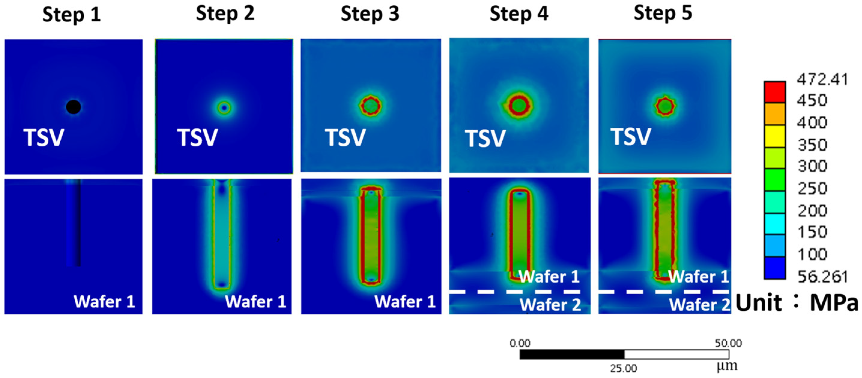
Figure 3 illustrates the mechanical stress distribution at each major process step. In Step 1, which involves TSV etching, the stress levels are minimal and uniformly distributed. This is expected, as the TSV trenches are not yet filled with copper (Cu), and thus the thermal mismatch between materials has not yet introduced significant stress. The structure remains mechanically stable at this stage. In Step 2, during the chemical mechanical planarization (CMP) process, stress begins to concentrate around the edges of the TSVs. The stress distribution is symmetric with respect to the TSV’s central axis, indicating that the dominant contributor is thermal stress arising from the coefficient of thermal expansion (CTE) mismatch between the surrounding materials, rather than mechanical abrasion from the CMP process itself. This observation suggests that thermal effects outweigh mechanical polishing forces in influencing stress behavior. Step 3, which involves the formation of the front-side redistribution layer (RDL) using aluminum (Al), shows a significant increase in stress near the TSVs. This increase is primarily attributed to the higher processing temperature of 400 °C, which amplifies the thermal stress due to CTE differences between Al, SiO
2, and Si. Additionally, localized stress concentrations are observed at the interface between the front-side RDL and the silicon substrate, particularly where SiO
2 is present. This is again due to the mismatch in thermal expansion properties between Si and SiO
2. In Steps 4 and 5, after the oxide bonding of two wafers and the completion of the back-side RDL process, the stress distribution remains concentrated around the TSV edges. These results confirm that the TSV perimeter is consistently the most vulnerable region to stress accumulation throughout the entire process flow. The analysis clearly indicates that the operating temperature at each process step is the primary factor influencing stress behavior in the system.
Figure 4 presents the equivalent stress along a radial path extending from the center of a TSV. In Step 1, the stress remains low, with a peak value of approximately 33 MPa, due to the absence of Cu filling. This result aligns with previous studies [
14], validating the accuracy of our simulation model. As the process progresses, the stress increases significantly. The yield strength of Si is approximately 165 MPa, and using a safety factor of 1.5, we define the critical stress threshold for the keep-out zone (KOZ) as 110 MPa. The stress peaks at the TSV edge, located about 3 μm from the center, and gradually decreases with distance. The stress falls below the KOZ threshold at a distance of approximately 7.5 μm from the TSV center. Therefore, the KOZ radius in this model is determined to be 7.5 μm, which is 1.5 times the TSV diameter. In
Figure 4, the radial stress profile is sampled along a straight path originating from the center of the TSV and extending outward into the silicon substrate. The TSV radius is 2.5 µm, and the reported peak stress at approximately 3 µm lies just beyond the TSV–Si interface, within the silicon region. This location corresponds to the area where thermal mismatch-induced stress is most pronounced.
We acknowledge that silicon is a brittle and anisotropic material, and that von Mises stress with a yield-based threshold may oversimplify KOZ estimation. In this study, we adopted a conservative stress limit (165 MPa with a safety factor of 1.5) as a first-order approximation, consistent with prior TSV modeling literature.
Interestingly, the stress profiles for Step 3 (blue line) and Step 4 (green line) are nearly identical, which can be attributed to the similar thermal conditions applied during these steps. This further reinforces the conclusion that thermal gradients, rather than mechanical processing, are the dominant contributors to stress accumulation in the 3DIC structure. To further explore the impact of TSV layout on mechanical reliability, we extended our simulation to include multiple TSVs with varying pitch distances.
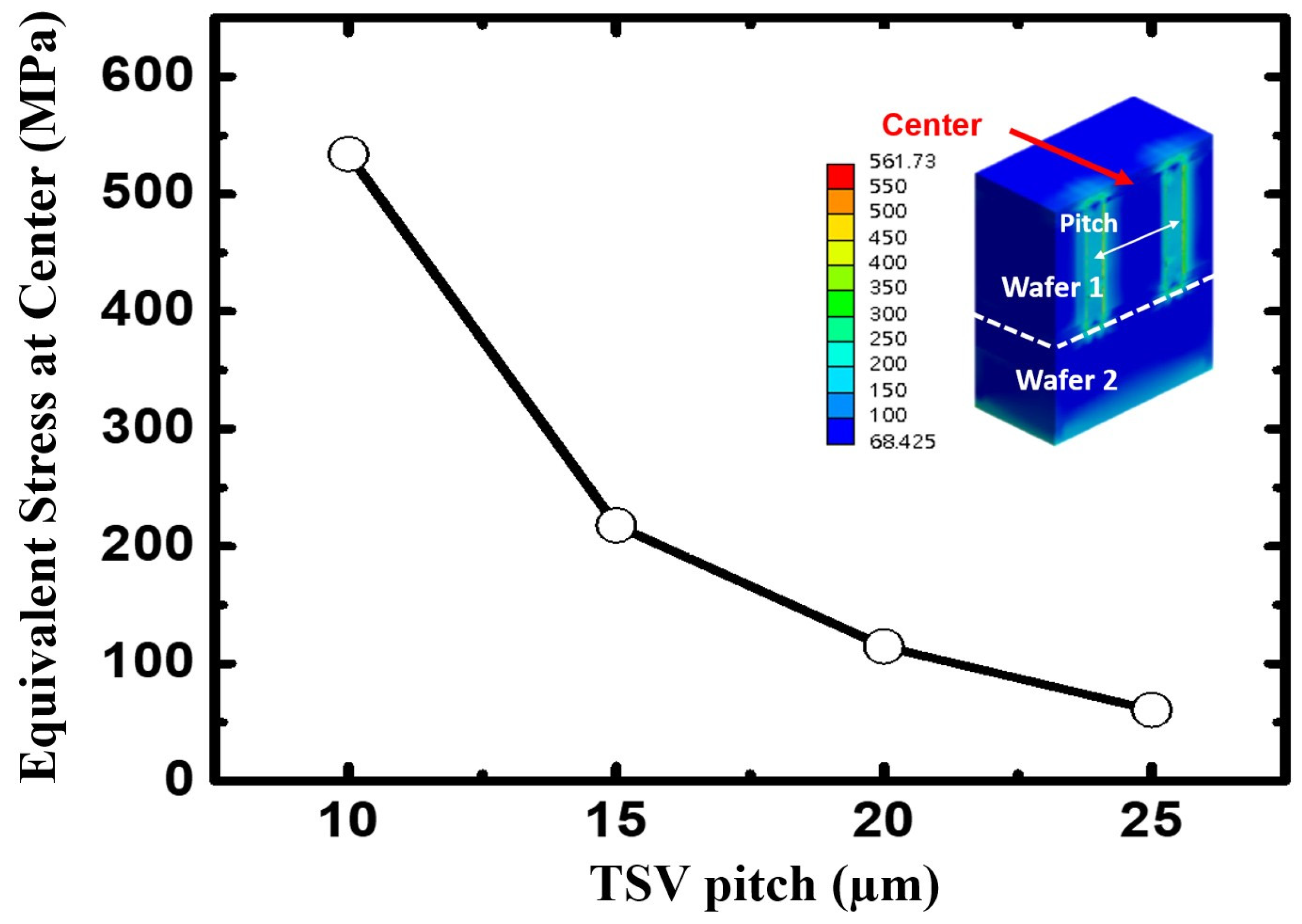
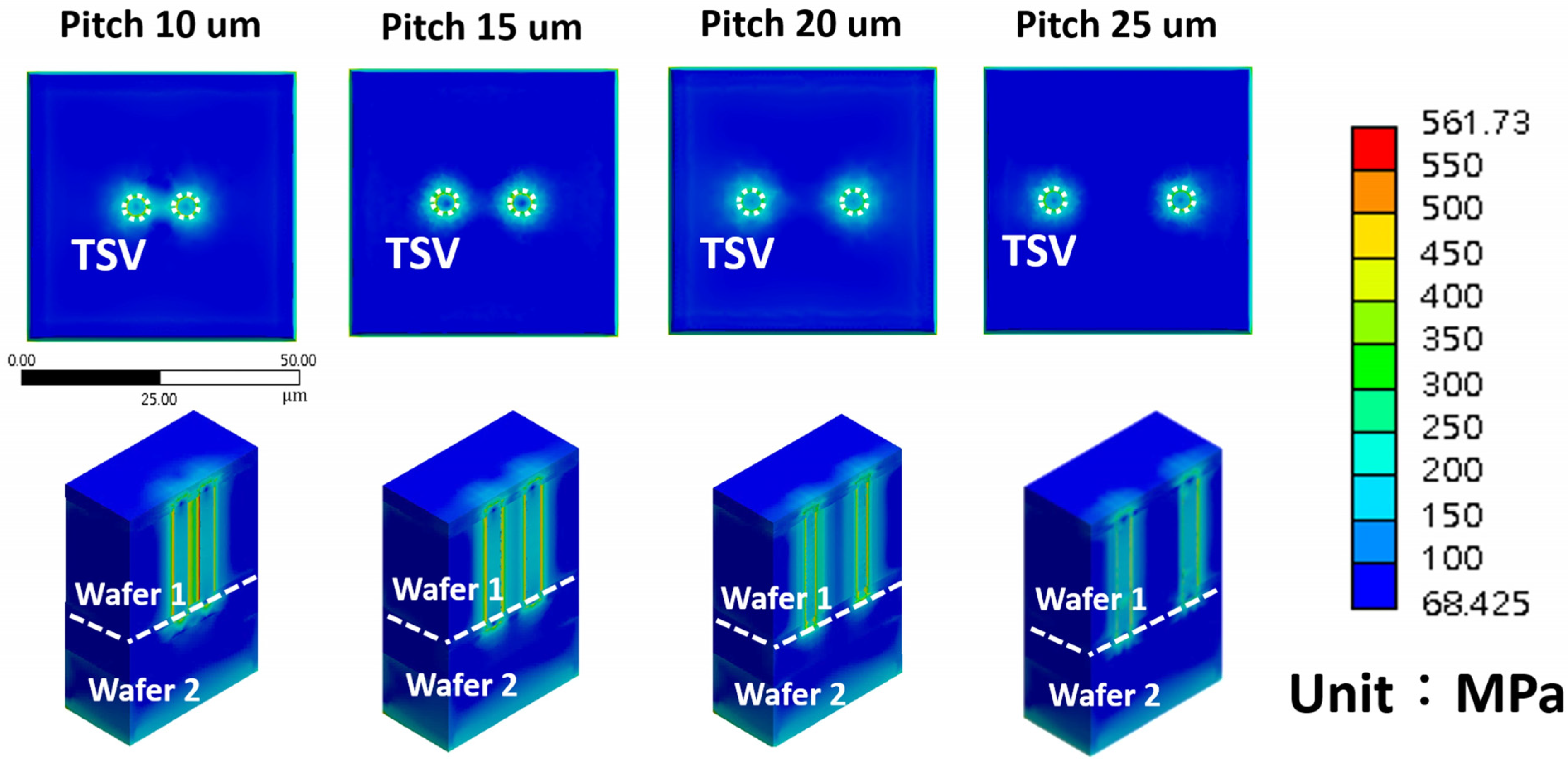
Figure 5 shows the stress distribution on the Si substrate surface and across a cross-sectional plane for a dual-TSV configuration. When the pitch is reduced to 10 μm, significant stress interaction is observed between adjacent TSVs. The maximum stress remains concentrated at the TSV edges, but additional stress appears in the region between the two vias, indicating mechanical coupling. As the pitch increases to 15 μm and 20 μm, the stress interaction between TSVs diminishes. At a pitch of 25 μm or greater, the stress between TSVs becomes negligible, and the stress fields behave independently. This trend is quantitatively summarized in
Figure 6, which plots the equivalent stress at the midpoint between two TSVs for various pitch values. Compared to the single TSV case, the presence of two closely spaced TSVs results in higher stress at the same radial distance due to overlapping stress fields. Consequently, the KOZ for the dual-TSV configuration expands to approximately 10 μm, representing a 33.3% increase over the 7.5 μm KOZ determined for the single TSV case. This finding highlights the importance of considering TSV pitch during layout design, as insufficient spacing can exacerbate stress-related reliability issues.
Although this study does not include lifetime or failure rate models, reliability is assessed through stress-based criteria. The KOZ is defined based on the critical stress threshold for silicon, and its variation with TSV pitch provides a practical indicator of mechanical reliability.
3.2. Thermal Characteristics
This study elucidates a fundamental trade-off inherent in TSV layout design: a wider TSV spacing, while beneficial for mitigating mechanical stress interactions and preserving structural integrity, can concurrently impede thermal dissipation due to a reduced overall copper density. Conversely, a closer TSV spacing significantly enhances thermal conductivity, thereby facilitating more efficient heat removal. However, this increased proximity concurrently amplifies the likelihood of detrimental stress coupling between adjacent TSVs, necessitating a larger Keep-Out Zone (KOZ) to ensure adequate mechanical reliability.
Consequently, identifying the optimal TSV pitch mandates a judicious and balanced consideration of both thermal and mechanical performance factors. Our simulation results indicate that a pitch ranging approximately from 20 to 25 μm presents a favorable compromise, effectively minimizing stress interactions while still capitalizing on the inherent thermal advantages offered by the copper within the TSVs. Future research endeavors will focus on exploring multi-objective optimization strategies to quantitatively define this intricate balance across a spectrum of varying design constraints and specific application requirements.
In addition to mechanical stress, thermal behavior is a critical factor in the reliability and performance of 3DIC systems.
Figure 7 presents the temperature profiles at each process step after a defined period of heat dissipation. Among all steps, Step 1 exhibits the lowest temperature, while Step 5 reaches the highest temperature, reflecting the cumulative thermal load introduced during the back-side RDL process. These results indicate that higher processing temperatures require longer cooling times to reach thermal equilibrium.
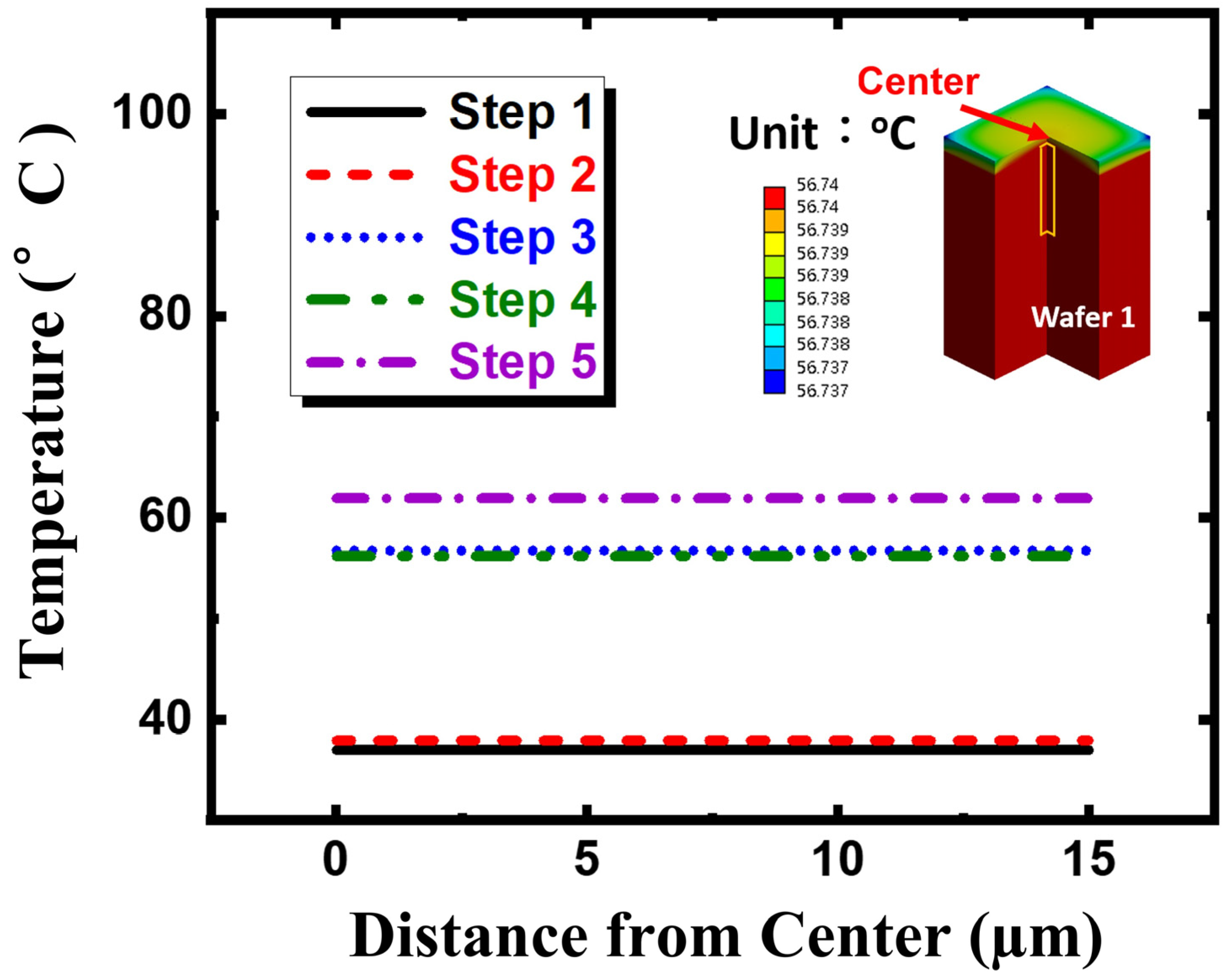
Figure 8 summarizes the temperature distribution along a radial path from the center to the edge of a TSV after cooling. The temperature variation along this path is minimal, with a deviation of less than 0.01%, indicating that the entire structure reaches a uniform temperature quickly. This uniformity suggests that despite differences in material properties and geometries, the thermal conductivity of the structure is sufficient to achieve rapid thermal balance across the device.
Figure 6.
Variation of Equivalent Stress in the 3D Oxide-Bonded Structure with Different TSV Pitches.
Figure 6.
Variation of Equivalent Stress in the 3D Oxide-Bonded Structure with Different TSV Pitches.
Figure 7.
Temperature contour plots for each process step in the 3D oxide-bonded stacking scheme.
Figure 7.
Temperature contour plots for each process step in the 3D oxide-bonded stacking scheme.
Figure 8.
Process-wise Temperature Profiles Across the TSV Center in the 3D Oxide-Bonded Structure.
Figure 8.
Process-wise Temperature Profiles Across the TSV Center in the 3D Oxide-Bonded Structure.
To further investigate the thermal behavior in multi-TSV configurations, we simulated temperature distributions for TSV pairs with varying pitch distances ranging from 10 μm to 25 μm.
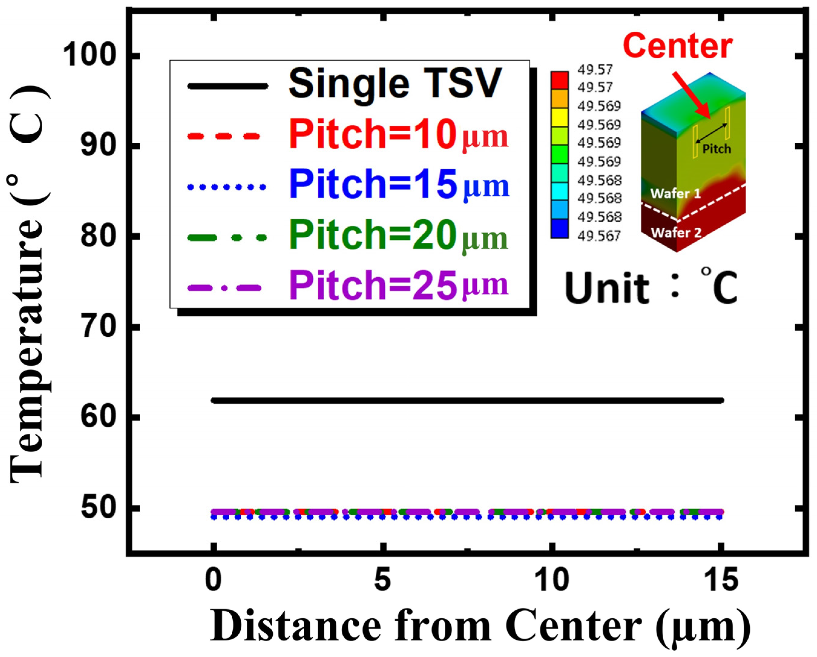
Figure 9 shows that the temperature distribution remains nearly constant at approximately 50 °C across all pitch values. This consistency implies that TSV pitch has a negligible effect on steady-state temperature distribution under the given thermal boundary conditions. However, when comparing single and multiple TSV configurations, a notable difference in thermal performance is observed.
Figure 10 compares the temperature profiles of single and dual-TSV structures. The results reveal that the temperature in the dual-TSV configuration is approximately 20% lower than in the single TSV case. This improvement is attributed to the increased thermal conduction paths provided by the additional Cu TSV, which enhances overall heat dissipation. The high thermal conductivity of Cu plays a crucial role in distributing and dissipating heat more effectively in multi-TSV systems. These findings underscore the dual role of TSVs in 3DICs—not only as electrical interconnects but also as thermal conduits. While closely spaced TSVs may introduce mechanical stress interactions, they also offer improved thermal performance. Therefore, an optimal TSV layout must balance these competing factors to ensure both mechanical reliability and efficient thermal management. The flat temperature distribution observed in
Figure 8 and
Figure 10 reflects the steady-state condition after thermal dissipation. Due to the high thermal conductivity of copper and the relatively short thermal paths in the modeled structure, the system reaches thermal equilibrium rapidly, resulting in minimal spatial temperature variation.
While the present study offers foundational insights into stress coupling and the evolution of the Keep-Out Zone (KOZ) by focusing on single and dual TSV (Through-Silicon Via) configurations, we recognize the need to extend this analysis to more complex TSV arrays. Configurations like 2 × 2 or 3 × 3 arrangements, for example, more closely represent the practical layouts found in advanced 3D integrated circuits. Therefore, our future work will involve expanding the current simulation framework to effectively model larger TSV clusters. This next step is crucial for gaining a more comprehensive understanding of multi-TSV interactions and their intricate effects on both mechanical reliability and thermal management in densely integrated systems.
While this study primarily relies on numerical simulations, the robustness and reliability of the presented results are substantiated by several key factors. Firstly, the developed simulation framework meticulously incorporates realistic process parameters and material properties, all of which are meticulously aligned with values extensively reported in the existing literature. Secondly, the simulated distributions of stress and temperature exhibit strong agreement with previously published experimental trends. This concordance is particularly evident in the accurate prediction of stress localization around TSV edges and the observed thermal uniformity across the simulated structure. Although direct experimental validation falls outside the scope of the current work, the consistent alignment of our findings with established physical behaviors and prior empirical studies significantly bolsters the credibility of our analysis.
4. Conclusions
In this study, we conducted a comprehensive simulation-based analysis of the thermo-mechanical behavior of a 3D integrated circuit (3DIC) structure fabricated using an oxide bonding scheme with Through-Silicon Vias (TSVs). By modeling each critical process step, we evaluated the evolution of mechanical stress and thermal characteristics throughout the fabrication flow. Our results demonstrate that thermal stress induced by temperature gradients—particularly due to the mismatch in the coefficients of thermal expansion (CTE) between materials—is significantly more influential than mechanical effects such as those introduced during the CMP process.
A key outcome of this work is the definition of the keep-out zone (KOZ), which is essential for ensuring device reliability. Based on the stress distribution analysis, we determined that the KOZ should extend to a distance approximately 1.5 times the TSV diameter from the TSV center, where the stress falls below the critical threshold for silicon.
Thermal simulations revealed that, despite variations in material properties and structural geometry, the temperature distribution across the device remains nearly uniform after cooling, indicating efficient thermal equilibrium. Furthermore, we investigated the impact of TSV pitch in multi-TSV configurations. Our findings show that closely spaced TSVs exhibit thermal stress interactions, resulting in a 33.3% increase in KOZ compared to single TSV structures. However, these configurations also offer improved thermal dissipation due to the high thermal conductivity of copper.
Although this study meticulously focuses on cylindrical TSVs (Through-Silicon Vias) with fixed diameters to establish fundamental principles, we recognize that practical 3DIC (Three-Dimensional Integrated Circuit) implementations often incorporate diverse via geometries. Structures like tapered or conical TSVs, for instance, can significantly influence stress distribution and thermal behavior due to their varying cross-sectional profiles. To broaden the practical relevance of our findings, future research will investigate the impact of these geometrical variations on Keep-Out Zone (KOZ) evolution and stress coupling. This will provide a more comprehensive understanding of the complex TSV-induced reliability challenges in advanced packaging.
Although this study relies primarily on simulation-based analysis, the robustness of our results is validated by benchmarking them against previously reported experimental trends, as shown in
Figure 4. The strong agreement between our simulated stress profiles and the reference experimental data provides compelling support for our modeling approach. This is especially evident in the accurate prediction of peak stress localization and the precise estimation of the Keep-Out Zone (KOZ). Such alignment significantly strengthens the overall credibility of our simulation framework.
Overall, this work provides critical insights into the reliability and thermal performance of 3DICs, enabling future optimization of TSV design, process parameters, and layout strategies for advanced semiconductor packaging. The findings also offer valuable guidance for the development of high-performance sensor devices, where mechanical stability and efficient heat dissipation are essential for ensuring long-term functionality and precision.
