Article

Electroluminescent Sensing Coating for On-Line Detection of Zero-Value Insulators in High-Voltage Systems

1
Electric Power Research Institute, Yunnan Power Gird Co., Ltd., Kunming 650217, China
2
State Key Laboratory of Electrical Insulation and Power Equipment, Xi’an Jiaotong University, Xi’an 710049, China
3
Key Laboratory of Engineering Dielectrics and Its Application, Harbin University of Science and Technology, Ministry of Education, Harbin 150080, China
*
Authors to whom correspondence should be addressed.
These authors contributed equally to this work.
Appl. Sci. 2025, 15(14), 7965; https://doi.org/10.3390/app15147965
Submission received: 1 June 2025 / Revised: 9 July 2025 / Accepted: 16 July 2025 / Published: 17 July 2025
(This article belongs to the Special Issue Advances in Electrical Insulation Systems)

Abstract

Featured Application

This paper introduces an electroluminescent sensing strategy for the real-time detection of zero-value insulators in high-voltage transmission systems. By integrating ZnS:Cu electroluminescent coatings onto insulator surfaces, this methodology provides a naked-eye-observable, on-line, diagnostic strategy for monitoring insulation health. Such an approach could be easily adapted to high-voltage equipment, offering convenient fault detection and maintenance capabilities in electrical infrastructures.

Abstract

In high-voltage transmission lines, insulators subjected to prolonged electromechanical stress are prone to zero-value defects, leading to insulation failure and posing significant risks to power grid reliability. The conventional detection method of spark gap is vulnerable to environmental interference, while the emerging electric field distribution-based techniques require complex instrumentation, limiting its applications in scenes of complex structures and atop tower climbing. To address these challenges, this study proposes an electroluminescent sensing strategy for zero-value insulator identification based on the electroluminescence of ZnS:Cu. Based on the stimulation of electrical stress, real-time monitoring of the health status of insulators was achieved by applying the composite of epoxy and ZnS:Cu onto the connection area between the insulator steel cap and the shed. Experimental results demonstrate that healthy insulators exhibit characteristic luminescence, whereas zero-value insulators show no luminescence due to a reduced drop in electrical potential. Compared with conventional detection methods requiring access of electric signals, such non-contact optical detection method offers high fault-recognition accuracy and real-time response capability within milliseconds. This work establishes a novel intelligent sensing paradigm for visualized condition monitoring of electrical equipment, demonstrating significant potential for fault diagnosis in advanced power systems.

1. Introduction

High-voltage transmission lines form the critical infrastructure for modern power systems, enabling efficient long-distance electricity transfer, essential for contemporary energy demands. Within these networks, insulators serve a dual function, providing mechanical support for overhead conductors while offering reliable electrical isolation between the conductors and the grounding structure [1,2,3]. However, prolonged exposure to electromechanical stress, environmental weathering, and cyclic electrical loads inevitably degrades insulator materials, leading to the formation of “zero-value defects”, which is a failure mode where insulators lose resistive properties due to internal cracks, surface contamination, or dielectric aging [4,5,6,7]. Such defects transform insulators into conductive pathways, causing leakage currents, localized heating, and flashover events that jeopardize grid stability and risk widespread power outages [8,9,10,11].
Conventional defect detection methods predominantly employ spark gap measurements, relying on manual auditory or visual identification of discharge phenomena [12,13,14]. While straightforward, this approach suffers from critical limitations: labor-intensive implementation, subjective interpretation vulnerable to human error, and susceptibility to ambient noise in operational environments [12,13,14]. Furthermore, its qualitative nature fails to quantify defect severity, hindering predictive maintenance strategies [15,16].
Recent advancements in electric field distribution analysis have emerged as a promising alternative. By correlating insulator defects with distortions in local electric field patterns, researchers aim to create a more objective diagnostic framework. However, existing electric field-based techniques often require sophisticated instrumentation, such as capacitive probes or computational simulations, which are impractical for large-scale deployment or real-time monitoring [17,18,19]. Additionally, these methods lack the ability to provide intuitive visual feedback, an essential feature for on-site decision-making by maintenance personnel [20,21].
The limitations of traditional approaches have spurred interest in novel sensing paradigms that combine high sensitivity, real-time operation, and user-friendly diagnostics. Among these, electroluminescent (EL) materials have gained attention due to their unique ability to convert electric field energy directly into visible light. This phenomenon, driven by the recombination of electron–hole pairs in semiconductor materials under an applied electric field, offers a compelling opportunity to visualize voltage variations without external power sources or complex electronics [22,23,24]. However, as shown in Table S1 [25,26,27,28,29], standard EL technologies primarily operate under low-voltage and benign environmental conditions, with a focus on luminous efficiency or color tuning. Conventional EL systems, including perovskite LEDs (CsPb(Br/Cl)3), quantum dot devices (MoS2@MoO3), and organic emitters (B/N-doped hydrocarbons), operate exclusively at low voltages and require precisely engineered electrode interfaces to generate luminescence. These materials face intrinsic limitations in high-voltage environments: perovskites degrade under humidity and UV exposure, hydrogels exhibit temperature-dependent performance collapse above 40 °C, and most systems necessitate hermetic sealing to prevent oxygen degradation, constraints that render them impractical for outdoor power infrastructure. While electroluminescent materials have seen significant advances in low-voltage applications, their implementation in high-voltage power equipment remains remarkably limited. This demands concurrent solutions to unique challenges, including ultra-high field endurance and dielectric integrity preservation, while maintaining EL functionality for fault diagnosis [30,31,32]. The few existing high-voltage applications primarily focus on GIS components, which explored EL-based field mapping for basin-type GIS insulators, but this work was confined to medium and low voltage electrical equipment in indoor environments and did not address transmission line monitoring challenges [33,34,35,36,37].
In response to these challenges, this study proposes an on-line monitoring sensing strategy for identifying zero-value insulators based on electroluminescence. The core innovation involves integrating copper-doped zinc sulfide (ZnS:Cu) electroluminescent powder into an epoxy coating, which is applied to the critical junction between the insulator’s steel cap and its ceramic or polymer shed. This region, which experiences concentrated mechanical and electrical stresses, serves as a sensitive indicator of insulator health. The primary objectives of this work are threefold: (1) developing and fabricating a durable EL composite coating capable of withstanding the harsh conditions of high-voltage transmission lines; (2) establishing a quantitative relationship between luminescent intensity and voltage magnitude, enabling fault severity assessment; and (3) validating the proposed method’s diagnostic accuracy, response speed, and practicality through comparative experiments.

2. Materials and Methods

Materials preparation: ZnS:Cu fluorescent powder was prepared by high-temperature solid-phase method. The specific preparation process is as follows: Firstly, ZnS and copper chloride (CuCl2) powder were mixed evenly in methanol at a molar ratio of 99:1 and wet-milled for 120 min until fully dried to obtain the precursor mixture. Secondly, the precursor mixture was placed in an alumina boat and compacted, and the temperature in the tube furnace was set at 1050 °C and held for 180 min. Then, the alumina boat was taken out of the tube furnace, placed in a muffle furnace, and adjusted to a temperature of 300 °C for annealing for 30 min. Finally, the obtained sample was re-ground, washed, and dried. A voltage-sensing coating based on ZnS:Cu EL material was prepared. First, E51 epoxy resin and crosslinking agent were mixed in a centrifugal mixer at a ratio of 9:5 and stirred at a stirring speed of 25 krad/min for 30 min for uniform mixing to obtain the mixed material. The 9:5 ratio ensures the curing reaction proceeds efficiently at ambient conditions, forming a densely crosslinked network that achieves full curing within hours at 25 °C. Then, ZnS:Cu was added to the mixed material with the mass ratio of 1:4. The mixed ZnS:Cu/epoxy mixture was stirred in a centrifugal mixer at a stirring speed of 25 krad/min for 10 min. Finally, the well-mixed coating was sprayed on the surface of the insulator to form a coating. ZnS:Cu EL powder will emit light under the irradiation of ultraviolet lamps. By spraying under ultraviolet lamps, the spraying effect can be observed in real time to ensure uniform spraying. To reduce the distortion of the electric field strength on the insulator surface caused by the coating, the coating should be as thin as possible, with a thickness aimed to approximately 0.1 mm. In controlled deposition processes, thickness is generally maintained as constant unless intentionally varied. Thickness variations across the deposited layer, however, are inevitable due to inherent limitations in manufacturing techniques. Substrate roughness, coating viscosity fluctuations, drying kinetics, or edge effects during deposition can create gradients.
Characterization: A 35 kV test transformer was used to apply voltage to both ends of the insulator. The rated capacity of the equipment was 100 kVA, the rated voltage was 35/0.4 kV, and the rated current was 2.86/250 A. One end of the insulator was connected to the high-voltage terminal of the transformer and the other end was connected to ground. The output voltage at the high-voltage terminal was controlled through a computer to change the voltage applied to the insulator, thereby controlling the luminescence and color change effect of the coating. The dielectric spectrum was performed with a concept 80 system (Novocontrol Technologies GmbH, Hundsangen, Germany) with 1 V AC voltage in the temperature range of −100–160 °C and frequency range of 10−1–106 Hz. The breakdown test was performed with 25 mm standard sphere-plate copper electrode in insulating oil with a voltage ramping rate of 1 kV/s. The surface flashover experiment of the insulator was carried out in an air environment; the interval between two consecutive surface discharges was 2 min. In each case, three samples were tested, and 11 flashover experiments were conducted on each insulator. With the use of a calibrated high-precision spectrometer (Ocean Insight HDX-VIS-NIR spectrometer), under the illumination of the standard light source D65, the sample to be tested was fixed on the test platform to ensure a flat surface and no interference from environmental stray light. The spectral reflectance/transmittance data of the sample within the wavelength range of 380–780 nm were collected by the spectrometer, and then the chromaticity coordinates (x, y) were derived and calibrated on the CIE 1964 chromaticity diagram. The experiment was repeated three times, and the average value was taken to ensure the reliability of the data.

3. Results and Discussion

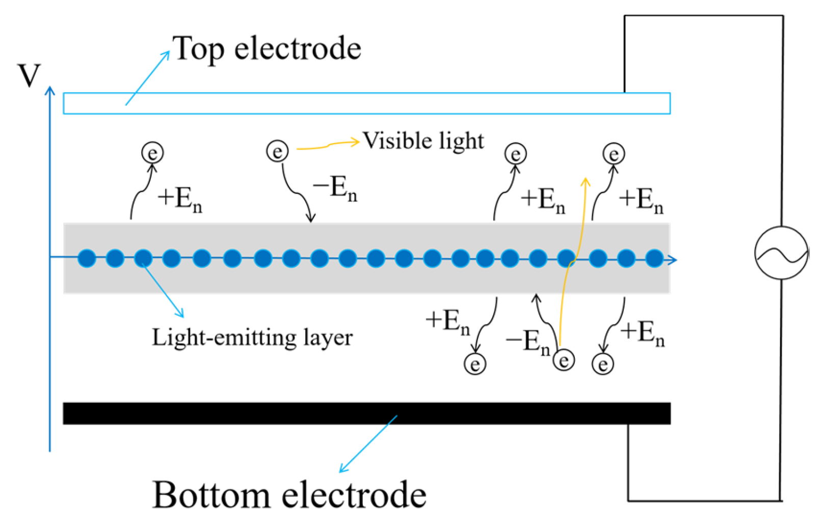
3.1. The Triggering Mechanism of EL in ZnS:Cu

ZnS:Cu is a classic type of intrinsic EL material; its EL process originates from the collision ionization and radiation recombination mechanism of carriers under a high electric field [38]. As shown in Figure 1, under an alternating electric field, electrons are injected into the ZnS:Cu light-emitting layer through the transparent electrode and the metal back electrode. When the applied electric field intensity reaches approximately 1 kV/mm, the carriers acquire sufficient kinetic energy under the acceleration of the electric field and undergo inelastic collisions with the Cu2+ luminescent centers in the lattice [39,40]. This process causes the electrons in the luminescent center to be excited to a metastable energy level and then return to the ground state through radiative transitions, releasing green photons with a wavelength of 505 nm [39,40]. The field-driven excitation mechanism provides the fundamental basis for utilizing ZnS:Cu in high-voltage sensing applications, where electric field strength can directly govern EL output.

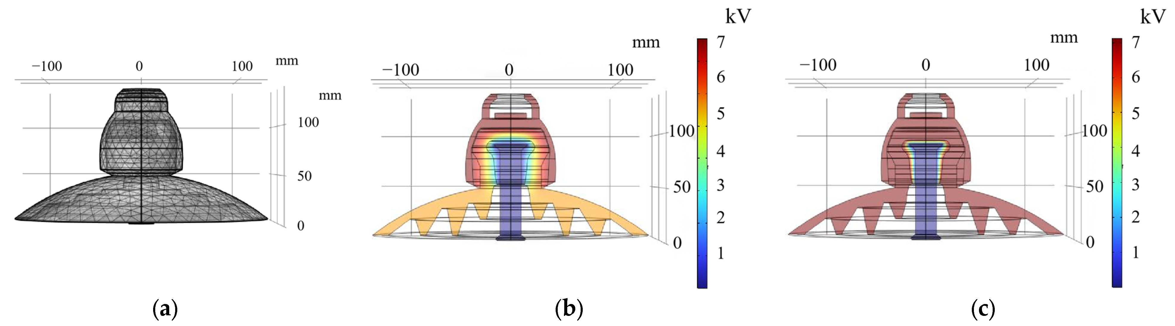
3.2. Voltage Distribution Simulation of Insulators and Insulator Strings

During the operation of high-voltage power systems, there is an obvious potential distribution on the surface of insulators. Obtaining a clear situation of the voltage distribution on the insulator is helpful for better understanding and formulating the insulator voltage characterization strategy based on EL coating. In this study, the finite element analysis (FEA) was employed to investigate the surface potential distribution characteristics under operational conditions by using the COMSOL Multiphysics platform (COMSOL 6.2).
The structural model of the insulator used in the simulation is shown in Figure 2a. The relative dielectric constant and electrical conductivity of the insulator’s shed, steel cap, steel foot, and cement-based bonded part were set according to the values detailed in Table 1, whose parameters reflect typical material properties derived from standardized testing data and literature benchmarks [41,42]. The zero-value defects were modeled by modifying the material parameters of cement and ceramic with a relative permittivity of 8000 and a conductivity of 0.1 S/m. The model adopts triangle meshing with adaptive refinement at material interfaces to resolve steep potential gradients while maintaining computational efficiency. Boundary conditions were defined to replicate operational scenarios: high-voltage terminal with 10 kV AC excitation (50 Hz), ground terminal with zero potential constraint, and atmospheric boundaries with floating potential with air dielectric properties. For an insulator with effective insulation performance, the simulated potential distribution reveals a characteristic nonlinear voltage gradient along the shed surface, as shown in Figure 2b. The steel cap-to-shed potential difference reaches 2.4 kV under 10 kV voltage. However, when the insulator is damaged and reaches a zero value state, as shown in Figure 2c, the potential difference between the steel cap and the shed decreases significantly (<100 V). In this case, the steel cap and the shed can basically be regarded as being at the same electrical potential.
To validate scalability to practical transmission line configurations, a 110 kV voltage-level insulator string comprising seven units was simulated. As shown in Figure 3a,b, the voltage division exhibits characteristic nonlinear distribution along the string for an insulator string with effective insulation performance. There is a potential difference of 17 kV between the steel cap of the terminal insulator and the shed, while there is a potential difference of 15 kv between the central insulators. This pattern is caused by the edge effect, amplified by the mutual capacitance between adjacent insulators. Conversely, the introduction of zero-value insulators dramatically redistributes voltages, as shown in Figure 3c,d. The potential difference between the two ends of the zero-value insulator drops sharply to less than 100 V, while the adjacent insulator experiences a surge to 20 kV. This redistribution adheres to Kirchhoff’s voltage law, as the zero-value insulator’s near-zero impedance forces neighboring insulators to compensate through elevated electric stresses. These simulations confirm that anomalous voltage redistribution provides a robust indicator for identifying zero-value insulators in the insulator string. This variation in potential difference provides the basic principle of using EL coating to detect zero-value insulators in this work. When the insulator performs with effective insulation, there is a potential difference between the steel cap and the shed, and this potential difference can drive the EL coating to glow. And for insulators with zero-value defects, zero-value defects cause the insulation resistance of the insulator to drop sharply and lose its insulation property.
The finite element simulations reveal a fundamental behavior in potential distribution: healthy insulators maintain substantial voltage gradients across their surfaces, while zero-value insulators exhibit near-equipotential conditions (<100 V) due to their collapsed impedance. This critical finding directly inspired our EL coating design strategy—by the application of the luminescent material at locations of maximum potential difference in functional insulators, the coating’s light emission becomes a direct visual indicator of insulation integrity.

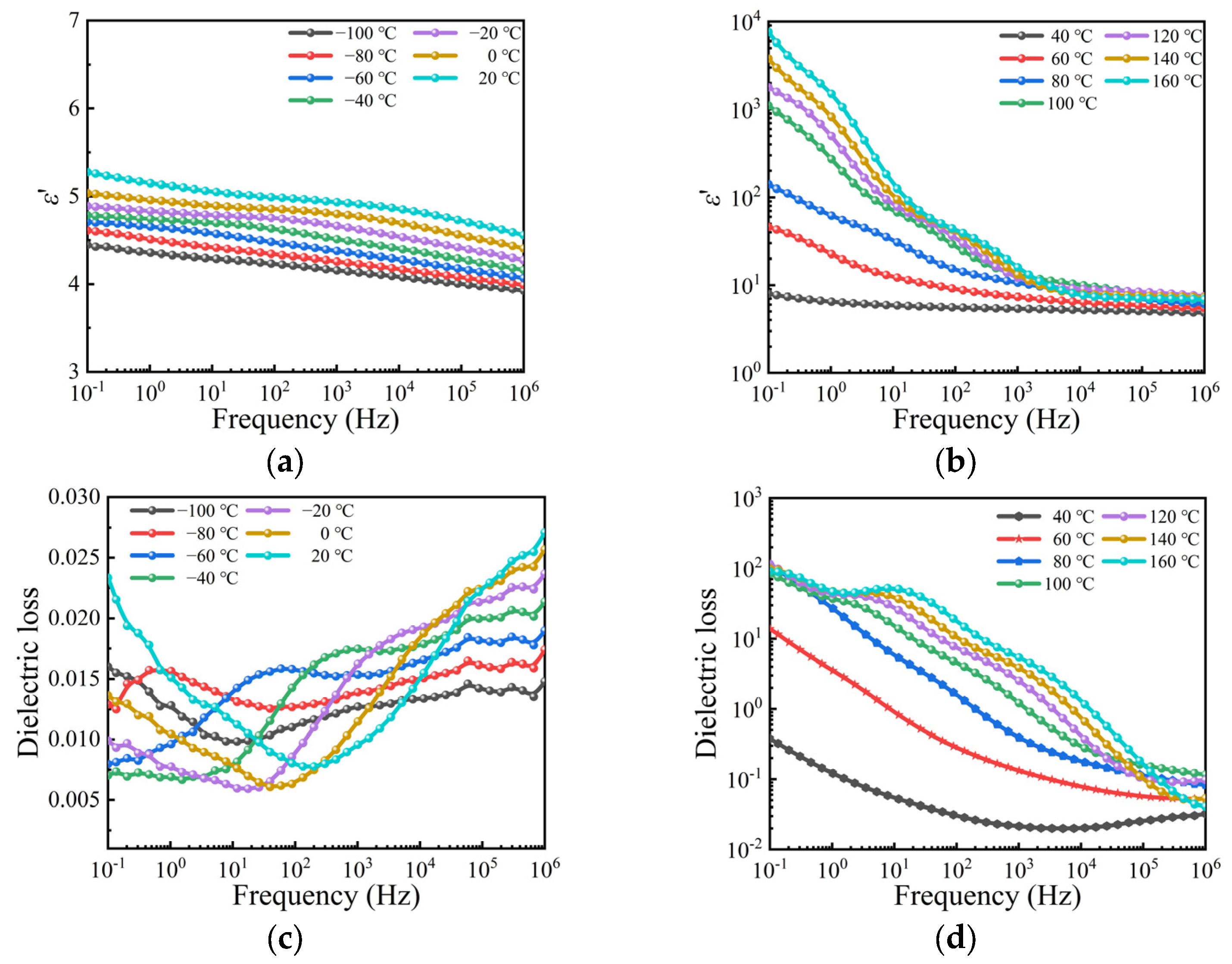
3.3. Dielectric Properties of the EL Coating

The dielectric stability of ZnS:Cu-doped epoxy composites constitutes a critical parameter governing their viability as functional coatings for high-voltage insulators [33,43]. To comprehensively evaluate this aspect, broadband dielectric spectroscopy was employed to characterize temperature- and frequency-dependent permittivity (εᵣ) and dielectric loss (tan δ) across operational ranges (−100~160 °C; 10−1~106 Hz), with results detailed in Figure 4. The dielectric constant (εr) profiles reveal three distinct thermal regimes influenced by dominant polarization processes, as shown in Figure 4a,b. At sub-ambient temperatures (−100~20 °C), εᵣ maintains exceptional stability within 4.5–5.5 across all frequencies (Figure 4a), while tan δ remains below 0.02 (Figure 4c). This thermodynamically constrained behavior arises from restricted molecular mobility below the material’s glass transition temperature (Tg), where dipolar orientation becomes kinetically inhibited [33,43]. Within the service temperature window (20~60 °C), εr at power frequencies (50~60 Hz) stabilizes at approximately 5–10, closely aligning with values reported for undoped epoxy systems, thus confirming that ZnS:Cu doping preserves the baseline capacitive voltage-division behavior without significantly distorting the dielectric response. At elevated temperatures (>60 °C), however, a sharp rise in εr is observed, particularly below 10 Hz, where values reach over 103. This anomalous behavior is attributed to the enhanced segmental chain mobility at the temperature over Tg.
In parallel, tan δ spectra delineate two distinct thermally activated relaxation processes, as shown in Figure 4c,d. The first, a β-relaxation process occurring in the −100~20 °C range, exhibits peak frequencies in the 102~103 Hz [33,43]. This relaxation is attributed to interfacial polarization at the filler–matrix boundaries, facilitated by the higher electron affinity of ZnS:Cu relative to the epoxy host. The second, a high-temperature α-relaxation process (120~160 °C), occurs at lower frequencies (100~102 Hz). This process is associated with epoxy chain reptation dynamics and coupled Zn2+ ionic conduction effects near the electrodes. The temperature-dependent dielectric loss behavior adheres to the Havriliak–Negami empirical relation [33,43].
Furthermore, the electrical conductivity measurements corroborate these dielectric transitions. Experimental data in Figure 5a,b shows that the coating’s conductivity remains stable and favorable below 40 °C, ensuring optimal insulation. However, as the temperature exceeds 40 °C, which is above Tg of the coating material, there is a noticeable increase in the coating’s conductivity. This rise stems from enhanced molecular mobility and the activation of charge carriers, which cases the material transitions to a more flexible state. Thus, the coating may not be applied to power equipment under high temperatures at this stage.
Breakdown field strength and flashover voltage along the surface are two other extremely important performance indicators of insulators. As shown in Figure 5c, the breakdown field strength is 36.48 kV/mm, meeting the required standards for effective high-voltage insulation. Additionally, experimental measurements of the flashover voltage of insulators coated with this material reveal a clear improvement in their performance, as shown in Figure 5d. When the insulator surface is coated with the paint, the flashover voltage increases from 35 kV for an uncoated insulator to 37 kV. This enhancement is indicative of the protective nature of the coating; by mitigating surface flashover, the coating significantly boosts the operational reliability of insulators under high-voltage conditions. As shown in Figure S1, the fracture surface exhibits excellent dispersion of ZnS:Cu particles within the epoxy matrix, with no observable agglomeration even at high magnification. The particles demonstrate uniform spatial distribution throughout the coating, which directly contributes to the material’s homogeneous luminescent output and stable dielectric properties. The SEM images further demonstrate intimate interfacial contact between ZnS:Cu particles and the epoxy matrix, with no visible voids or delamination at the filler–matrix boundaries. This dense microstructure accounts for the coating’s high breakdown strength and enhanced flashover resistance, as it prevents localized field concentration that could initiate electrical trees or surface discharges. This nanoscale characterization bridges the gap between material design and macroscopic performance, explaining why the coating achieves both reliable EL response and robust insulation properties. As for the aging life of the coating, while accelerated aging datasets require future validation, industrial evidence suggests the E51 epoxy-based coating retains structural/dielectric stability for 2–5 years in moderate outdoor environments [44,45,46].
In summary, the EL coating has stable εr, low dielectric loss, high breakdown field strength, and flashover suppression capability within the working temperature range. These capabilities ensure the insulation reliability of the EL coating itself and make it suitable for insulator detection under high-voltage operation.

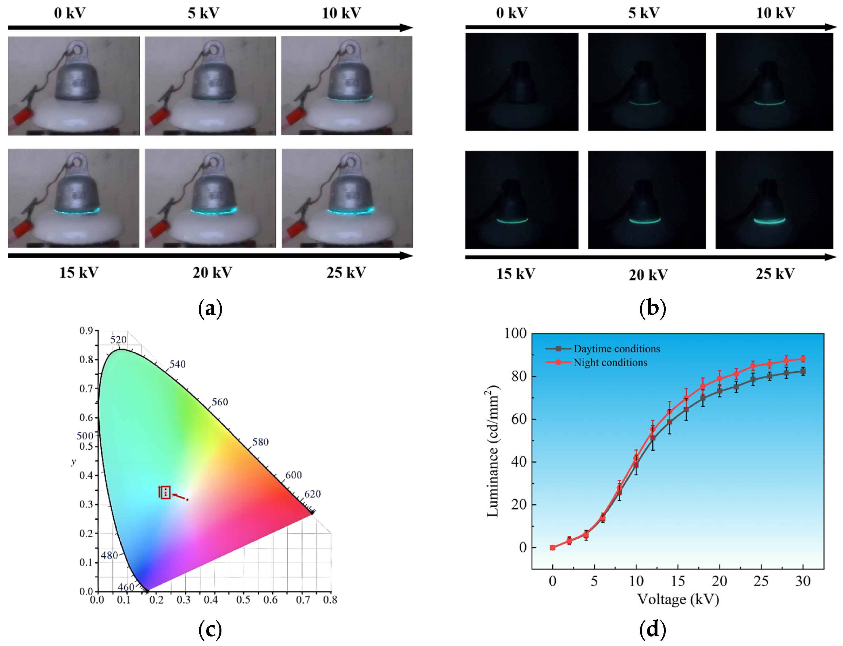
3.4. Experiment of the Insulators with EL Coating

The luminescent intensity and spectral stability of EL materials under high electric fields are pivotal for their application in EL-voltage sensing systems. To quantitatively assess the relationship between electric field strength, luminous intensity, and chromaticity characteristics, the EL behavior of ZnS:Cu–epoxy composite films was systematically characterized using a custom-designed ball-sphere electrode configuration, as schematically illustrated in Figure 6a. Experimental observations reveal that a distinct EL response emerges at an applied voltage of approximately 2 kV, marking the onset of visible light emission from the composite film. As the applied voltage increases, the luminescent intensity progressively enhances, and at voltages exceeding 5 kV, the entire film exhibits a pronounced and uniform blue-green glow. The corresponding chromaticity coordinates are shown in Figure 6b, confirming the spectral stability of the emission across varying field intensities. Further analysis of the voltage-dependent luminous response, as presented in Figure 6c, indicates a clear saturation behavior beyond 6 kV. In this regime, the luminous intensity plateaus, suggesting that most of tge ZnS:Cu particles have reached excitation equilibrium, and the charge injection processes governing radiative recombination have stabilized. Overall, these results demonstrate that the ZnS:Cu–epoxy composite not only exhibits robust electroluminescence under high-voltage excitation but also maintains chromatic stability and intensity reproducibility, reinforcing its potential in advanced optoelectronic and energy-autonomous sensing platforms.
In order to evaluate the feasibility of EL coating sensing and indicating the voltage magnitude endured by insulators, different voltages were applied to both ends of EL-coated insulators with a surface coating thickness of 120 μm, and the luminescence phenomenon of EL coating under different voltages was observed. Under daytime indoor conditions (Figure 7a), the coating exhibited a clear blue-green EL response when the applied voltage exceeded a threshold of 5 kV. The luminous intensity increased progressively with higher voltages, demonstrating a strong voltage dependence. Nighttime experiments (Figure 7b) revealed a similar trend, with luminescent intensity enhancing as voltage increased. Notably, the chromaticity coordinates of the emitted light remained stable at (0.26, 0.31) across all tested voltages (Figure 7c), confirming the consistency and reproducibility of the luminescent color—a critical feature for practical sensing applications. The specific numerical relationship between voltage and luminous intensity (Figure 7d) displayed a linear increase within the 5–20 kV range. In particular, when the applied voltage exceeds 22 kV, the intensity saturated, suggesting that carrier injection had reached equilibrium, and further voltage increases did not significantly enhance light output. Interestingly, nighttime measurements recorded a 10% higher luminous intensity than daytime observations at identical voltages. This discrepancy is attributed to the absence of ambient stray light at night, allowing more accurate detection of the coating’s intrinsic luminescence.
The coating’s metrological performance was rigorously validated through comparisons between experimental measurements and finite element simulations. The developed model successfully predicted voltage distributions across test insulators using luminescence intensity as input, achieving a mean error of 10% (Table 2). The model demonstrated improved accuracy at higher voltages, with errors decreasing to approximately 7% in the 15~20 kV range, indicating particular suitability for typical transmission line operating conditions. This close agreement between experimental and simulated results confirms the coating’s dual capability as both a visual indicator and quantitative measurement tool for insulator voltage monitoring. The observed 10% mean error between measured and simulated voltages (Table 2) stems from compounded uncertainties in instrumentation, environmental variables, and model simplifications. Instrumentation limitations primarily from the Ocean Insight HDX-VIS-NIR spectrometer’s NIST-traceable calibration uncertainty (±3%), dark noise (±0.1 cd/mm2), and daytime stray light suppression, which collectively contributed ~4.2% to the total error, with dominant effects below 10 kV, where signal-to-noise ratios were suboptimal. Model assumptions introduced a ~3.3% discrepancy, notably from simulating a uniform relative permittivity and omitting edge-field enhancements at the steel cap–shed junction. Additionally, coating thickness variations and ZnS:Cu dispersion heterogeneity contributed ~2.5% through localized electric field distortions. Voltage-dependent trends further contextualize these errors: higher discrepancies at 5–10 kV align with instrumentation limitations under low-photon-flux conditions, while improved accuracy at 15–20 kV reflects enhanced signal stability where model simplifications became the residual error source. To address these limitations, future implementations will employ electrospray deposition for thickness control, integrate real-time temperature compensation using εr-T relationships from Figure 4, and adopt high-dynamic-range photodetectors to mitigate saturation effects.
The above experimental results confirm that the EL coatings can effectively sense the voltage applied to individual insulators. To further validate their capability for detecting zero-value insulators, we conducted tests on a string of seven insulators (including two zero-value insulators) under an applied voltage of 110 kV. The voltage distribution across each insulator and the corresponding luminescence intensity of the coating were measured simultaneously (Figure 8). The coating exhibited distinct luminescence responses that clearly differentiated between functional and zero-value insulators. While healthy insulators showed measurable luminescence intensities proportional to their voltage loads, the zero-value insulators displayed negligible luminescence, as evidenced by the detailed inset in Figure 8. This direct correlation between luminescence absence and zero-voltage conditions demonstrates the coating’s effectiveness in identifying faulty insulators within a string.
To quantitatively assess this relationship, we performed simulations based on the measured luminescence intensities to predict the voltage distribution across the insulator string. The simulated results showed excellent agreement with experimental measurements, with discrepancies consistently below 10%. Notably, the simulation accurately predicted the near-zero voltage condition of the defective insulators, further validating the reliability of this approach. The combined experimental and simulation results demonstrate that this approach can significantly enhance the safety monitoring of high-voltage transmission lines, providing both immediate visual feedback and precise quantitative data for maintenance decisions. The robust performance under actual operating conditions (110 kV) and the consistent sub 10% error in voltage prediction highlight the technical viability of this solution for practical grid applications. Based on the above experimental phenomena, we also propose an innovative solution for future field applications. Field inspections deploy UAVs equipped with multispectral imaging to capture real-time electroluminescent responses (e.g., chromatic shift from blue-green to colorless under abnormal fields) in ZnS:Cu–epoxy coatings on live 110 kV insulators, enabling simultaneous defect localization with infrared thermography.

4. Conclusions

In summary, this study establishes ZnS:Cu EL coating with potential as an on-line sensing strategy for zero-value insulator detection in high-voltage transmission systems. Critically, we demonstrate a quantitative relationship between applied voltage and EL intensity, characterized by an activation threshold at 2 kV and performance saturation above 6 kV, with blue-green luminescence characteristics within CIE coordinates of 0.19–0.32. Crucially, integrating this EL coating at the steel cap–shed interface preserves the insulator’s core dielectric functionality, maintaining a stable permittivity of 5.5 at 50 Hz/20 °C and low dielectric loss tangent < 0.02 under ambient conditions. The coating enhances insulator flashover voltage from 35 kV to 37 kV, with a characteristic breakdown strength of 37 kV/mm, thereby meeting practical insulation requirements. Validation on 110 kV insulator strings robustly confirms the coating’s diagnostic capability, where insulators of effective insulation performance show naked-eye-observable, voltage-proportional light emission, while zero-value insulators exhibit near-zero luminescence due to collapsed potential differences. Comparative analysis of simulated and experimental voltage distributions reveals <10% deviation, confirming the reliability of the strategy for real-time on-line monitoring proposed here. Consequently, this work establishes an intelligent paradigm for the on-line health monitoring of insulators by merging passive sensing with optical diagnostics, proposes an emerging strategy for the design of self-diagnostic power infrastructure, and potentially contributes to the maintenance strategies in next-generation smart power grids.

Supplementary Materials

The following supporting information can be downloaded at: https://www.mdpi.com/article/10.3390/app15147965/s1, Figure S1: SEM image of the cross-section of the EL coating sample; Figure S2: EL spectra of the coating sample at varied voltages; Table S1: Performances of representative EL devices; Table S2: Luminance and CIE coordinate of the EL coating sample under 0–8 kV; Table S3: Luminance and CIE coordinate of the EL coating on the insulator under 0–25 kV and different light conditions.

Author Contributions

Conceptualization, Y.N. and Y.J.; data curation, D.C. and J.S.; formal analysis, Y.N., Y.J. and P.W.; funding acquisition, Y.N. and Y.H.; investigation, J.S.; methodology, P.W. and D.C.; project administration, Y.N. and Y.H.; resources, Y.H. and Y.Z.; software, P.W.; supervision, Y.H., Y.Z. and S.L.; validation, Y.H., Y.Z. and S.L.; visualization, D.C.; writing—original draft, Y.N., Y.J. and P.W.; writing—review and editing, Y.H., Y.Z. and S.L. All authors have read and agreed to the published version of the manuscript.

Funding

This research is funded by China Southern Power Grid (YNKJXM20240497), the National Natural Science Foundation of China (52477028), the Key R&D Projects in Shaanxi Province (2025CY-YBXM-133), the Youth Fund of State Key Laboratory of Electrical Insulation and Power Equipment (EIPE23407), and the Fundamental Research Funds for the Central Universities (sxzy012023180).

Institutional Review Board Statement

Not applicable.

Informed Consent Statement

Not applicable.

Data Availability Statement

The original contributions presented in this study are included in the article/Supplementary Material. Further inquiries can be directed to the corresponding author(s).

Conflicts of Interest

Authors Yongjie Nie and Daoyuan Chen were employed by the company Yunnan Power Gird Co., Ltd. The remaining authors declare that the research was conducted in the absence of any commercial or financial relationships that could be construed as a potential conflict of interest.

References

  1. He, M.; Qin, L.; Deng, X.; Liu, K. MFI-YOLO: Multi-Fault Insulator Detection Based on an Improved YOLOv8. IEEE Trans. Power Deliv. 2024, 39, 168–179. [Google Scholar] [CrossRef]
  2. Hauschild, W. Critical Review of Voltages Applied for Quality-Acceptance and Diagnostic Field Tests on High-Voltage and Extra-High-Voltage Cable Systems. IEEE Electr. Insul. Mag. 2013, 29, 16–25. [Google Scholar] [CrossRef]
  3. Wang, H.; Zhang, Y.; Lin, W.; Wei, W. Transregional Electricity Transmission and Carbon Emissions: Evidence from Ultra-High Voltage Transmission Projects in China. Energy Econ. 2023, 123, 106751. [Google Scholar] [CrossRef]
  4. Sadykova, D.; Pernebayeva, D.; Bagheri, M.; James, A. IN-YOLO: Real-Time Detection of Outdoor High Voltage Insulators Using UAV Imaging. IEEE Trans. Power Deliv. 2020, 35, 1599–1601. [Google Scholar] [CrossRef]
  5. Li, Y.; Zhu, X.; Li, B.; Zeng, J.; Wang, S. Discriminative Features Based Comprehensive Detector for Defective Insulators. Energy AI 2024, 17, 100387. [Google Scholar] [CrossRef]
  6. Yang, L.; Fan, J.; Liu, Y.; Li, E.; Peng, J.; Liang, Z. A Review on State-of-the-Art Power Line Inspection Techniques. IEEE Trans. Instrum. Meas. 2020, 69, 9350–9365. [Google Scholar] [CrossRef]
  7. Sun, J.; Song, S.; Zheng, J.; Li, Z.; Huo, J.; Wang, Y.; Xiao, P.; Akram, S.; Qin, D. A Review on Surface Flashover Phenomena at DC Voltage in Vacuum and Compressed Gas. IEEE Trans. Dielect. Electr. Insul. 2022, 29, 1–14. [Google Scholar] [CrossRef]
  8. Li, Z.; Liu, J.; Ohki, Y.; Chen, G.; Gao, H.; Li, S. Surface Flashover in 50 Years: Theoretical Models and Competing Mechanisms. High Volt. 2023, 8, 853–877. [Google Scholar] [CrossRef]
  9. Meng, X.; Mei, H.; Yin, F.; Wang, L. The Development of the Streamer Discharge to Flashover Along the Dielectric Surfaces. IEEE Trans. Dielect. Electr. Insul. 2023, 30, 1733–1742. [Google Scholar] [CrossRef]
  10. Han, P.; Pan, Z.; Mao, S.; Ye, Y.; Tang, J.; Pan, C. Understanding the Effect of SiC/Epoxy Coating on Surface Flashover under DC Voltage: From Surface Charge Accumulation. J. Phys. D Appl. Phys. 2023, 56, 405106. [Google Scholar] [CrossRef]
  11. Mizuno, Y.; Maeda, M.; Kondo, K. Flashover Risk-Based Probabilistic Design of Transmission Line Insulators under Contamination Conditions. IEEE Trans. Power Deliv. 2023, 38, 3611–3620. [Google Scholar] [CrossRef]
  12. Zeng, Z.; Guo, P.; Zhang, R.; Zhao, Z.; Bao, J.; Wang, Q.; Xu, Z. Review of Aging Evaluation Methods for Silicone Rubber Composite Insulators. Polymers 2023, 15, 1141. [Google Scholar] [CrossRef] [PubMed]
  13. Liu, Y.; Liu, D.; Huang, X.; Li, C. Insulator Defect Detection with Deep Learning: A Survey. IET Gener. Trans. Dist. 2023, 17, 3541–3558. [Google Scholar] [CrossRef]
  14. Liu, Y.; Guo, Y.; Fan, Y.; Zhou, J.; Li, Z.; Xiao, S.; Zhang, X.; Wu, G. Optical Imaging Technology Application in Transmission Line Insulator Monitoring: A Review. IEEE Trans. Dielect. Electr. Insul. 2024, 31, 3120–3132. [Google Scholar] [CrossRef]
  15. Mantach, S.; Lutfi, A.; Moradi Tavasani, H.; Ashraf, A.; El-Hag, A.; Kordi, B. Deep Learning in High Voltage Engineering: A Literature Review. Energies 2022, 15, 5005. [Google Scholar] [CrossRef]
  16. Rathod, V.B.; Kumbhar, G.B.; Bhalja, B.R. Partial Discharge Detection and Localization in Power Transformers Based on Acoustic Emission: Theory, Methods, and Recent Trends. IETE Tech. Rev. 2022, 39, 540–552. [Google Scholar] [CrossRef]
  17. Yang, C.; Guo, Y.; Shi, Z.; Li, B.; Zhang, X.; Xiao, S.; Wu, G. Discharge Characteristics of Roof Insulators in Strong Wind and Sand Environment: A Review. IEEE Trans. Dielect. Electr. Insul. 2024, 31, 3231–3242. [Google Scholar] [CrossRef]
  18. Faizol, Z.; Zubir, F.; Saman, N.M.; Ahmad, M.H.; Rahim, M.K.A.; Ayop, O.; Jusoh, M.; Majid, H.A.; Yusoff, Z. Detection Method of Partial Discharge on Transformer and Gas-Insulated Switchgear: A Review. Appl. Sci. 2023, 13, 9605. [Google Scholar] [CrossRef]
  19. Akbar, G.; Di Fatta, A.; Rizzo, G.; Ala, G.; Romano, P.; Imburgia, A. A Detailed Review of Partial Discharge Detection Methods for SiC Power Modules Under Square-Wave Voltage Excitation. Energies 2024, 17, 5793. [Google Scholar] [CrossRef]
  20. Kumar, H.; Shafiq, M.; Kauhaniemi, K.; Elmusrati, M. A Review on the Classification of Partial Discharges in Medium-Voltage Cables: Detection, Feature Extraction, Artificial Intelligence-Based Classification, and Optimization Techniques. Energies 2024, 17, 1142. [Google Scholar] [CrossRef]
  21. Meitei, S.N. Partial Discharge Detection Using Piezoelectric Sensors on Power Transformer: A Review. IEEE Sens. J. 2024, 24, 13730–13742. [Google Scholar] [CrossRef]
  22. Zhu, Y.; Jiang, Y.; Cao, F.; Wang, P.; Ke, J.; Liu, J.; Nie, Y.; Li, G.; Wei, Y.; Lu, G.; et al. Space Charge-Induced Electrofluorochromic Behavior for C12-BTBT-Based Thin-Film Devices. J. Mater. Chem. C 2025, 10, 1039. [Google Scholar]
  23. Del Prado Santamaría, R.; Dhimish, M.; Dos Reis Benatto, G.A.; Kari, T.; Poulsen, P.B.; Spataru, S.V. From Indoor to Daylight Electroluminescence Imaging for PV Module Diagnostics: A Comprehensive Review of Techniques, Challenges and AI-Driven Advancements. Micromachines 2025, 16, 437. [Google Scholar] [CrossRef] [PubMed]
  24. Liu, W.; Wang, G.; Wang, S. Intrinsically Stretchable Electroluminescent Materials and Devices. CCS Chem. 2024, 6, 1360–1379. [Google Scholar] [CrossRef]
  25. Zhou, W.; Shen, Y.; Cao, L.; Lu, Y.; Tang, Y.; Zhang, K.; Ren, H.; Xie, F.; Li, Y.; Tang, J. Manipulating Ionic Behavior with Bifunctional Additives for Efficient Sky-Blue Perovskite Light-Emitting Diodes. Adv. Funct. Mater. 2023, 33, 2301452. [Google Scholar] [CrossRef]
  26. Bai, W.; Shi, S.; Lin, T.; Zhou, T.; Xuan, T.; Xie, R.-J. Near-Unity Cyan-Green Emitting Lead-Free All-Inorganic Cesium Copper Chloride Phosphors for Full-Spectrum White Light-Emitting Diodes. Adv. Photon. Res. 2021, 2, 200158. [Google Scholar] [CrossRef]
  27. Bastami, N.; Soheyli, E.; Arslan, A.; Sahraei, R.; Yazici, A.F.; Mutlugun, E. Nanowire-Shaped MoS2@MoO3 Nanocomposites as a Hole Injection Layer for Quantum Dot Light-Emitting Diodes. ACS Appl. Electron. Mater. 2022, 4, 3849–3859. [Google Scholar] [CrossRef]
  28. Cai, T.; Li, F.; Jiang, Y.; Liu, X.; Xia, X.; Wang, X.; Peng, J.; Wang, L.; Daoud, W.A. In Situ Inclusion of Thiocyanate for Highly Luminescent and Stable CH3NH3PbBr3 Perovskite Nanocrystals. Nanoscale 2019, 11, 1319–1325. [Google Scholar] [CrossRef]
  29. Guo, J.; Li, Z.; Tian, X.; Zhang, T.; Wang, Y.; Dou, C. Diradical B/N-Doped Polycyclic Hydrocarbons. Angew. Chem. Int. Edit. 2023, 62, e202217470. [Google Scholar] [CrossRef]
  30. Chun, F.; Wang, F. Recent Advances in Perovskite-Based Flexible Electroluminescent Devices. ACS Nano 2024, 18, 25939–25965. [Google Scholar] [CrossRef]
  31. Tadesse, M.G.; Lübben, J.F. Recent Progress in Self-Healable Hydrogel-Based Electroluminescent Devices: A Comprehensive Review. Gels 2023, 9, 250. [Google Scholar] [CrossRef] [PubMed]
  32. Xu, Y.; Wang, Q.; Cai, X.; Li, C.; Jiang, S.; Wang, Y. Frontier Molecular Orbital Engineering: Constructing Highly Efficient Narrowband Organic Electroluminescent Materials. Angew Chem. Int. Ed. 2023, 62, e202312451. [Google Scholar] [CrossRef] [PubMed]
  33. Zhu, Y.; Qiao, N.; Dong, S.; Qu, G.; Chen, Y.; Lu, W.; Qin, Z.; Li, D.; Wu, K.; Nie, Y.; et al. Side-Chain Engineering of Polystyrene Dielectrics Toward High-Performance Photon Memories and Artificial Synapses. Chem. Mater. 2022, 34, 6505–6517. [Google Scholar] [CrossRef]
  34. Jia, Y.; Ji, S.; Bu, Z.; Yang, X.; Li, S.; Zhu, L. An Insulation Monitoring Method for Transformer Windings Based on Electroluminescence Effect. IEEE Trans. Dielect. Electr. Insul. 2023, 30, 1294–1301. [Google Scholar] [CrossRef]
  35. Ji, S.; Jia, Y.; Yang, X.; Liu, Z.; Zhu, L. A Method for Measuring Electric Field Distribution Along Insulator Surfaces Based on Electroluminescence Effect and Its Image Processing Algorithm. IEEE Trans. Dielect. Electr. Insul. 2022, 29, 939–947. [Google Scholar] [CrossRef]
  36. Xia, B.; Zhu, M.-X.; Guo, X.-B.; Qi, X.-W.; Yao, H.-B.; Xing, Z.-H. High Permittivity Electroluminescence Coating for Improving Flashover Strength and Visualizing Surface Defects. J. Phys. D Appl. Phys. 2025, 58, 055503. [Google Scholar] [CrossRef]
  37. Lai, Y.-S.; Hsieh, C.-C.; Liao, T.-W.; Huang, C.-Y.; Kuo, C.-F.J. Deep Learning-Based Automatic Defect Detection of Photovoltaic Modules in Infrared, Electroluminescence, and Red–Green–Blue Images. Energ. Convers. Manag. 2025, 332, 119783. [Google Scholar] [CrossRef]
  38. Pandey, T.; Singh, A.; Kaundal, R.S.; Pandey, V. Cation Exchange Doping by Transition and Non-Transition Metals: Embracing Luminescence for Band Gap Tunability in a ZnS Lattice. New J. Chem. 2024, 48, 1009–1035. [Google Scholar] [CrossRef]
  39. Wang, J.; Yu, J.; Wang, X.; Wang, L.; Li, B.; Shen, D.; Kang, Q.; Chen, L. Functional ZnS:Mn(II) Quantum Dot Modified with L-Cysteine and 6-Mercaptonicotinic Acid as a Fluorometric Probe for Copper(II). Microchim. Acta 2018, 185, 420. [Google Scholar] [CrossRef]
  40. Xu, J.; Li, Y.; Yao, Y.; Ding, Y.; Tan, Y.; Hu, G.; Zhang, S.; Zeng, L. A Stimulus-Responsive Optoelectronic Skin from Photonic Crystal. Adv. Opt. Mater. 2025, 13, 2500094. [Google Scholar] [CrossRef]
  41. Uckol, H.I.; Karaca, B.; Ilhan, S. DC and AC Electric Field Analysis and Experimental Verification of a Silicone Rubber Insulator. Electr. Eng. 2020, 102, 503–514. [Google Scholar] [CrossRef]
  42. Zhao, X.; Yang, X.; Hu, J.; Wang, H.; Yang, H.; Li, Q.; He, J.; Xu, Z.; Li, X. Grading of Electric Field Distribution of AC Polymeric Outdoor Insulators Using Field Grading Material. IEEE Trans. Dielect. Electr. Insul. 2019, 26, 1253–1260. [Google Scholar] [CrossRef]
  43. Zhu, Y.; Fan, Y.; Li, S.; Wei, P.; Li, D.; Liu, B.; Cui, D.; Zhang, Z.; Li, G.; Nie, Y.; et al. Soluble Poly(4-Fluorostyrene): A High-Performance Dielectric Electret for Organic Transistors and Memories. Mater. Horiz. 2020, 7, 1861–1871. [Google Scholar] [CrossRef]
  44. Starkova, O.; Gaidukovs, S.; Platnieks, O. Prediction of Viscoelastic Properties of Epoxy/Graphene Oxide Nanocomposites: Time-Temperature-Water Ageing Superposition. Polym. Degrad. Stabil. 2023, 214, 110400. [Google Scholar] [CrossRef]
  45. Ma, J.; Yang, Y.; Wang, Q.; Deng, Y.; Yap, M.; Chern, W.K.; Oh, J.T.; Chen, Z. Degradation and Lifetime Prediction of Epoxy Composite Insulation Materials under High Relative Humidity. Polymers 2023, 15, 2666. [Google Scholar] [CrossRef]
  46. Sukesh Babu, M.; Sarathi, R.; Imai, T.; Tanaka, T. Influence of Gamma Irradiation and Water Aging on the Space Charge Characteristics of Epoxy Micro-Nano Composites. Polymers 2021, 13, 964. [Google Scholar] [CrossRef]
Figure 1. The triggering mechanism of EL in ZnS:Cu.
Applsci 15 07965 g001
Figure 2. Simulation of electric field distributions in insulators. (a) Constructed insulator structure for simulation. (b) Electrical potential distributions of insulator with effective insulation performance. (c) Electrical potential distributions of zero-value insulator.
Applsci 15 07965 g002
Figure 3. Voltage distributions of an insulator string containing 7 insulators. (a) Voltage and (b) electrical potential distributions of an insulator string with 7 insulators of effective insulation performance. (c) Voltage and (d) electrical potential distributions of an insulator string containing 2 zero-value insulators.
Applsci 15 07965 g003
Figure 4. Frequency-dependent dielectric spectra of ZnS:Cu-doped epoxy composite coating. Variations of dielectric constant in (a) −100~20 °C, (b) −40~160 °C. Variations of dielectric loss in (c) −100~20 °C, (d) −40~160 °C.
Applsci 15 07965 g004
Figure 5. Electric conductivity and insulation performances of ZnS:Cu-doped epoxy composite coating. Frequency dependent electrical conductivity in (a) −100~20 °C, (b) −40~160 °C. (c) The AC breakdown performances. (d) The AC flashover voltages of insulators.
Applsci 15 07965 g005
Figure 6. Electroluminescence performances of the EL material. (a) Demonstration of electroluminescence under voltages of 0~6 kV. (b) CIE chromaticity diagrams of the light-emitting layer under voltages of 0~6 kV. (c) The luminous intensity of the light-emitting layer under voltages of 0~8 kV.
Applsci 15 07965 g006
Figure 7. Electroluminescence performances of ZnS:Cu coating on insulators (a) Demonstration of electroluminescence at voltages of 0~25 kV in indoor conditions. (b) Demonstration of electroluminescence at voltages of 0~25 kV in nighttime conditions. (c) Electroluminescence CIE of the coating at voltages of 0~25 kV. (d) Electroluminescence intensity of the coating on insulators at voltages of 0~30 kV.
Applsci 15 07965 g007
Figure 8. The EL result of the coating in the insulator string.
Applsci 15 07965 g008
Table 1. Simulation parameters of insulator.
MaterialAirCeramicCementSteel
Relative dielectric constant16141
Electrical conductivity1 × 10−41 × 10−81 × 10−91 × 107
Table 2. Measurement errors of the voltage across insulators at different voltage levels.
Electroluminous
Brightness
(cd/mm2)
Voltage Subjected to the Coating
(kV)
Simulated Voltage Subjected to the Insulator
(kV)
Actual Voltage Subjected to the Insulator
(kV)
Error Rate
(%)
3.160.451.8129.67
5.821.114.42410.45
13.561.385.4669.38
25.942.188.92811.54
38.652.309.24107.63
51.232.7611.21126.59
58.763.7815.18148.42
64.523.7114.86167.15
69.844.7619.24186.87
73.215.1821.19205.96
Disclaimer/Publisher’s Note: The statements, opinions and data contained in all publications are solely those of the individual author(s) and contributor(s) and not of MDPI and/or the editor(s). MDPI and/or the editor(s) disclaim responsibility for any injury to people or property resulting from any ideas, methods, instructions or products referred to in the content.

