

Simultaneous Submicron Temperature Mapping of Substrate and Channel in P-GaN/AlGaN/GaN HEMTs Using Raman Thermometry

 ,
, 
Abstract
1. Introduction
2. Materials and Methods
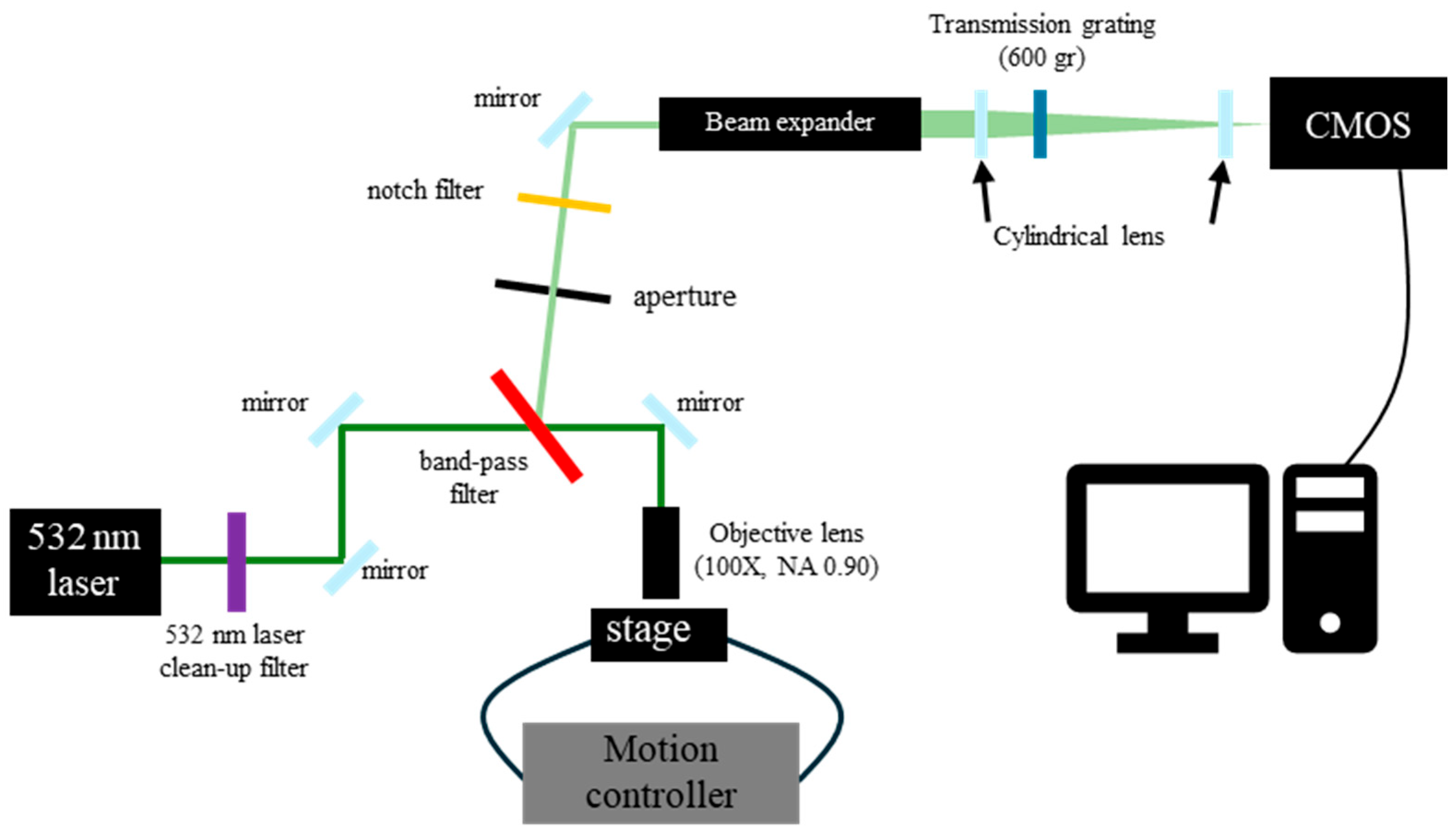
2.1. Modified Raman Spectroscopy Setup
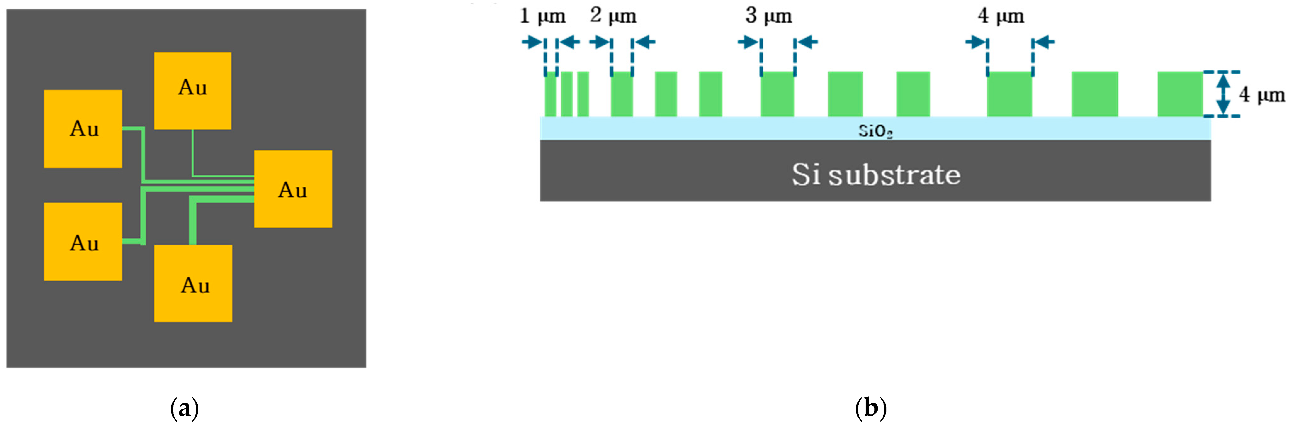
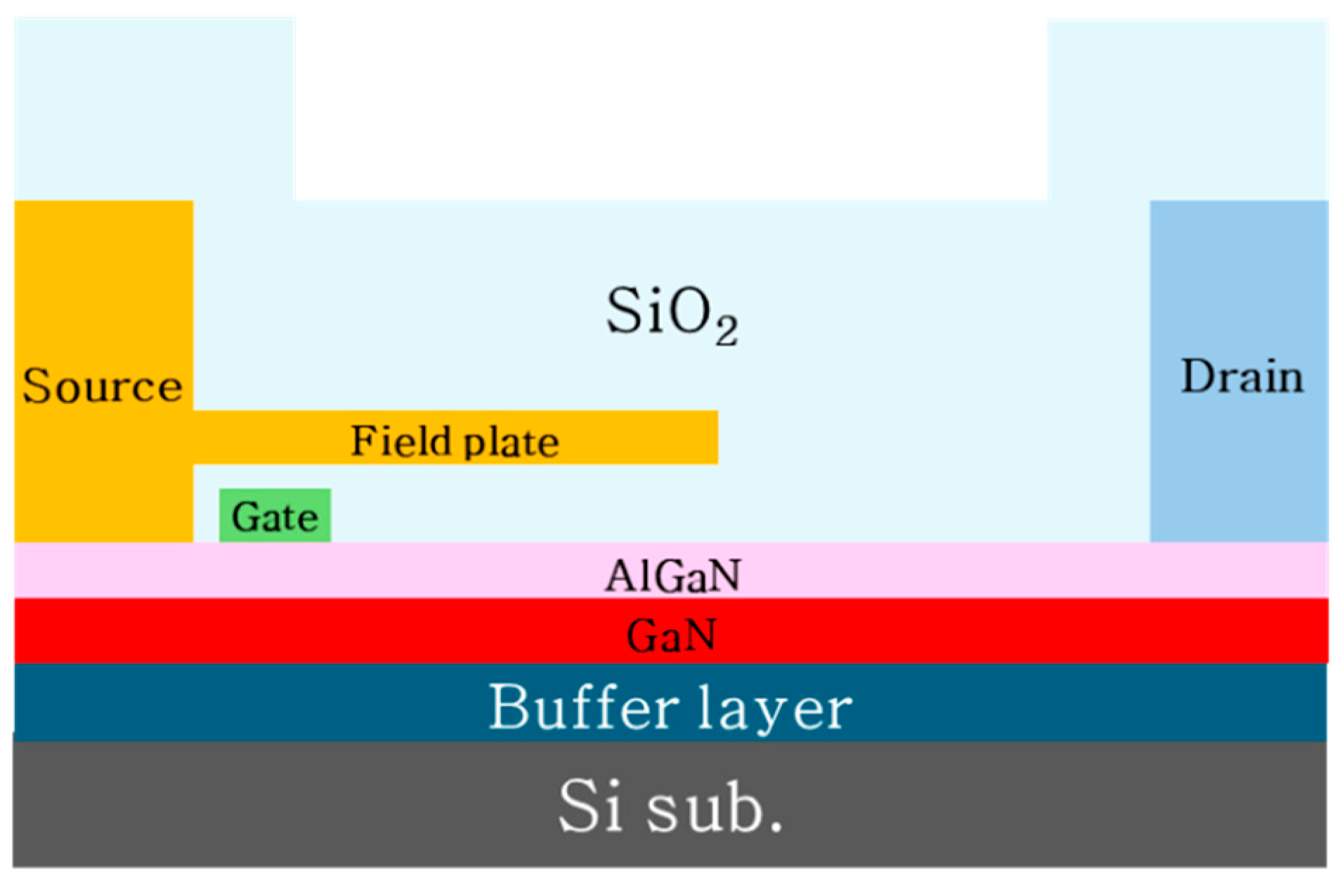
2.2. Sample
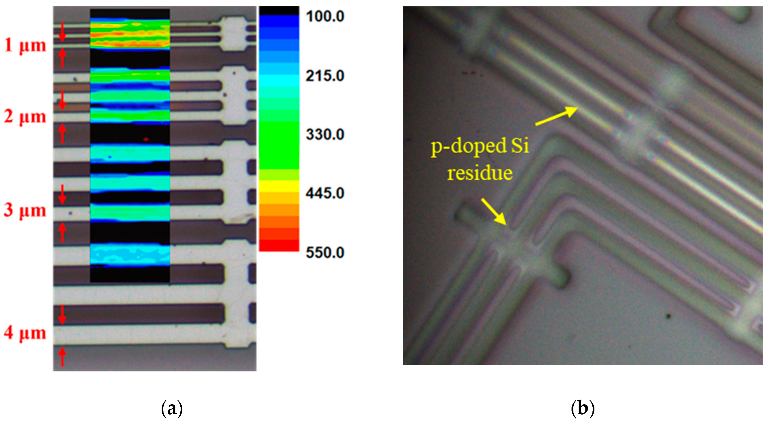
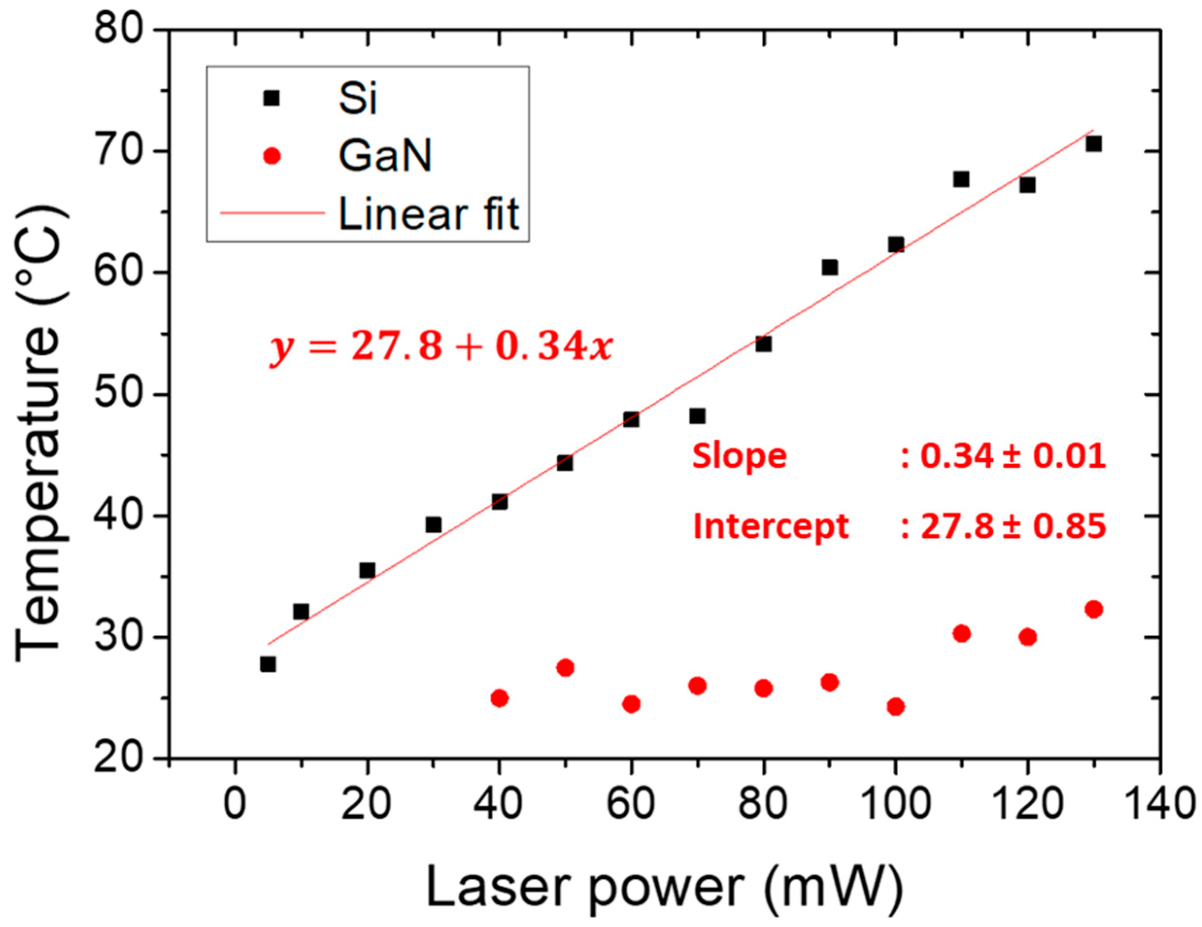
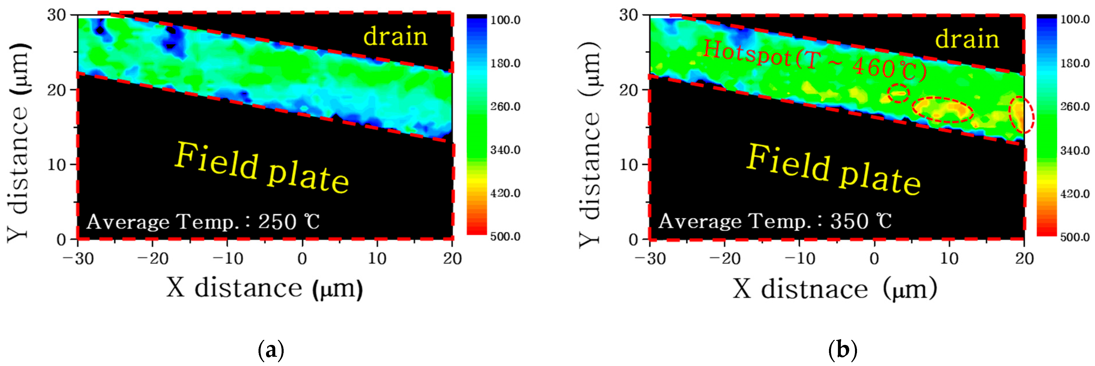
3. Results
4. Conclusions
Author Contributions
Funding
Institutional Review Board Statement
Informed Consent Statement
Data Availability Statement
Conflicts of Interest
Abbreviations
| 2DEG | 2-dimensional electron gas |
| HEMT | High electron mobility transistor |
| IR | Infrared |
| SOI | Silicon on insulator |
References
- He, J.; Cheng, W.C.; Wang, Q.; Cheng, K.; Yu, H.; Chai, Y. Recent advances in GaN-based power HEMT devices. Adv. Electron. Mater. 2021, 7, 2001045. [Google Scholar] [CrossRef]
- Keshmiri, N.; Wang, D.; Agrawal, B.; Hou, R.; Emadi, A. Current status and future trends of GaN HEMTs in electrified transportation. IEEE Access 2020, 8, 70553–70571. [Google Scholar] [CrossRef]
- Guo, H.; Duan, B.; Wu, H.; Yang, Y. Breakdown mechanisms of power semiconductor devices. IETE Technical Review 2019, 36, 243–252. [Google Scholar] [CrossRef]
- Roccaforte, F.; Fiorenza, P.; Greco, G.; Nigro, R.L.; Giannazzo, F.; Iucolano, F.; Saggio, M. Emerging trends in wide band gap semiconductors (SiC and GaN) technology for power devices. Microelectron. Eng. 2018, 187, 66–77. [Google Scholar] [CrossRef]
- Bose, B.K. Power electronics-a technology review. Proc. IEEE 1992, 80, 1303–1334. [Google Scholar] [CrossRef]
- Chen, K.J.; Häberlen, O.; Lidow, A.; lin Tsai, C.; Ueda, T.; Uemoto, Y.; Wu, Y. GaN-on-Si power technology: Devices and applications. IEEE Trans. Electron Devices 2017, 64, 779–795. [Google Scholar] [CrossRef]
- Chen, J.-T.; Bergsten, J.; Lu, J.; Janzén, E.; Thorsell, M.; Hultman, L.; Rorsman, N.; Kordina, O. A GaN–SiC hybrid material for high-frequency and power electronics. Appl. Phys. Lett. 2018, 113, 041605. [Google Scholar] [CrossRef]
- Chen, P.; Zhang, R.; Zhao, Z.M.; Xi, D.J.; Shen, B.; Chen, Z.Z.; Zhou, Y.G.; Xie, S.Y.; Lu, W.F.; Zheng, Y.D. Growth of high quality GaN layers with AlN buffer on Si (1 1 1) substrates. J. Cryst. Growth 2001, 225, 150–154. [Google Scholar] [CrossRef]
- Comyn, R.; Chenot, S.; Alouani, W.E.; Nemoz, M.; Frayssinet, E.; Damilano, B.; Cordier, Y. AlGaN/GaN/AlGaN DH-HEMTs Grown on a Patterned Silicon Substrate. Phys. Status Solidi 2018, 215, 1700642. [Google Scholar] [CrossRef]
- Leszczynski, M.; Prystawko, P.; Plesiewicz, J.; Dmowski, L.; Litwin-Staszewska, E.; Grzanka, S.; Grzanka, E.; Roccaforte, F. Comparison of Si. Sapphire, SiC, and GaN Substrates for HEMT Epitaxy. ECS Trans. 2013, 50, 163. [Google Scholar] [CrossRef]
- Saito, W.; Kuraguchi, M.; Takada, Y.; Tsuda, K.; Omura, I.; Ogura, T. High breakdown voltage undoped AlGaN-GaN power HEMT on sapphire substrate and its demonstration for DC-DC converter application. IEEE Trans. Electron Devices 2004, 51, 1913–1917. [Google Scholar] [CrossRef]
- Zhao, D.; Xu, S.; Xie, M.; Tong, S.; Yang, H. Stress and its effect on optical properties of GaN epilayers grown on Si (111). 6H-SiC (0001), and c-plane sapphire. Appl. Phys. Lett. 2003, 83, 677–679. [Google Scholar] [CrossRef]
- Guo, Y.B.; Bhat, K.P.; Aravamudhan, A.; Hopkins, D.C.; Hazelmyer, D.R. High Current and Thermal Transient Design of a SiC SSPC for Aircraft Application. In Proceedings of the 2011 Twenty-Sixth Annual IEEE Applied Power Electronics Conference and Exposition (APEC), Fort Worth, TX, USA, 6–11 March 2011; pp. 1290–1297. [Google Scholar]
- Ozpineci, B.; Tolbert, L.M.; Islam, S.K.; Hasanuzzaman, M. System impact of silicon carbide power devices. Int. J. High Speed Electron. Syst. 2002, 12, 439–448. [Google Scholar] [CrossRef]
- Jez, A.; Danilchenko, B.A.; Boćkowski, M.; Grzegory, I.; Krukowski, S.; Suski, T.; Paszkiewicz, T. Thermal conductivity of GaN crystals in 4.2–300 K range. Solid State Commun. 2003, 128, 69–73. [Google Scholar]
- Slack, G.A.; Schowalter, L.J.; Morelli, D.; Freitas, J.A., Jr. Some effects of oxygen impurities on AlN and GaN. J. Cryst. Growth 2002, 246, 287–298. [Google Scholar] [CrossRef]
- Chen, X.; Boumaiza, S.; Wei, L. Self-heating and equivalent channel temperature in short gate length GaN HEMTs. IEEE Trans. Electron Devices 2019, 66, 3748–3755. [Google Scholar] [CrossRef]
- Choi, S.; Heller, E.R.; Dorsey, D.; Vetury, R.; Graham, S. The impact of bias conditions on self-heating in AlGaN/GaN HEMTs. IEEE Trans. Electron Devices 2012, 60, 159–162. [Google Scholar] [CrossRef]
- Nigam, A.; Bhat, T.N.; Rajamani, S.; Dolmanan, S.B.; Tripathy, S.; Kumar, M. Effect of self-heating on electrical characteristics of AlGaN/GaN HEMT on Si (111) substrate. AIP Adv. 2017, 7, 085015. [Google Scholar] [CrossRef]
- Qin, Y.; Chai, C.; Li, F.; Liang, Q.; Wu, H.; Yang, Y. Study of self-heating and high-power microwave effects for enhancement-mode p-gate GaN HEMT. Micromachines 2022, 13, 106. [Google Scholar] [CrossRef]
- Alomari, M.; Dussaigne, A.; Martin, D.; Grandjean, N.; Gaquiere, C.; Kohn, E. AlGaN/GaN HEMT on (111) single crystalline diamond. Electron. Lett. 2010, 46, 1. [Google Scholar] [CrossRef]
- Gajewski, D.A.; Lewis, R.D.; Decker, B.M. Analysis and resolution of a thermally accelerated early life failure mechanism in a 40áV GaN FET. Microelectron. Reliab. 2014, 54, 2675–2681. [Google Scholar] [CrossRef]
- Martínez, P.; Letz, S.; Maset, E.; Zhao, D. Failure analysis of normally-off GaN HEMTs under avalanche conditions. Semicond. Sci. Technol. 2020, 35, 035007. [Google Scholar] [CrossRef]
- Pomeroy, J.W.; Uren, M.J.; Lambert, B.; Kuball, M. Operating channel temperature in GaN HEMTs: DC versus RF accelerated life testing. Microelectron. Reliab. 2015, 55, 2505–2510. [Google Scholar] [CrossRef]
- Rossetto, I.; Meneghini, M.; Hilt, O.; Bahat-Treidel, E.; De Santi, C.; Dalcanale, S.; Wuerfl, J.; Zanoni, E.; Meneghesso, G. Time-dependent failure of GaN-on-Si power HEMTs with p-GaN gate. IEEE Trans. Electron Devices 2016, 63, 2334–2339. [Google Scholar] [CrossRef]
- Zanoni, E.; Meneghini, M.; Chini, A.; Marcon, D.; Meneghesso, G. AlGaN/GaN-based HEMTs failure physics and reliability: Mechanisms affecting gate edge and Schottky junction. IEEE Trans. Electron Devices 2013, 60, 3119–3131. [Google Scholar] [CrossRef]
- Zanoni, E.; Meneghini, M.; Meneghesso, G.; Bisi, D.; Rossetto, I.; Stocco, A. Reliability and failure physics of GaN HEMT, MIS-HEMT and p-gate HEMTs for power switching applications: Parasitic effects and degradation due to deep level effects and time-dependent breakdown phenomena. In Proceedings of the 2015 IEEE 3rd Workshop on Wide Bandgap Power Devices and Applications (WiPDA), Blacksburg, VA, USA, 2–4 November 2015; pp. 75–80. [Google Scholar]
- Albright, G.C.; Stump, J.A.; Li, C.; Kaplan, H. Emissivity-corrected infrared thermal pulse measurement on microscopic semiconductor targets. In Proceedings Volume 4360, Thermosense XXIII; SPIE: Bellingham, WA, USA, 2001; pp. 103–111. [Google Scholar]
- Avenas, Y.; Dupont, L.; Khatir, Z. Temperature measurement of power semiconductor devices by thermo-sensitive electrical parameters—A review. IEEE Trans. Power Electron. 2011, 27, 3081–3092. [Google Scholar] [CrossRef]
- Baker, N.; Dupont, L.; Munk-Nielsen, S.; Iannuzzo, F.; Liserre, M. IR camera validation of IGBT junction temperature measurement via peak gate current. IEEE Trans. Power Electron. 2016, 32, 3099–3111. [Google Scholar] [CrossRef]
- Christofferson, J.; Shakouri, A. Thermal measurements of active semiconductor micro-structures acquired through the substrate using near IR thermoreflectance. Microelectron. J. 2004, 35, 791–796. [Google Scholar] [CrossRef]
- Kaplan, H. Practical Applications of Infrared Thermal Sensing and Imaging Equipment; SPIE Press: Bellingham, WA, USA, 2007. [Google Scholar]
- Boué, C.; Fournier, D. Cost-effective infrared thermography protocol for 40 μm spatial resolution quantitative microelectronic imaging. Infrared Phys. Technol. 2006, 48, 122–129. [Google Scholar] [CrossRef]
- Sarua, A.; Ji, H.; Kuball, M.; Uren, M.J.; Martin, T.; Hilton, K.P.; Balmer, R.S. Integrated micro-Raman/infrared thermography probe for monitoring of self-heating in AlGaN/GaN transistor structures. IEEE Trans. Electron Devices 2006, 53, 2438–2447. [Google Scholar] [CrossRef]
- Braun, J.L.; Olson, D.H.; Gaskins, J.T.; Hopkins, P.E. A steady-state thermoreflectance method to measure thermal conductivity. Rev. Sci. Instrum. 2019, 90, 024905. [Google Scholar] [CrossRef] [PubMed]
- Mun, J.; Kim, S.W.; Kato, R.; Hatta, I.; Lee, S.H.; Kang, K.H. Measurement of the thermal conductivity of TiO2 thin films by using the thermo-reflectance method. Thermochim. Acta 2007, 455, 55–59. [Google Scholar] [CrossRef]
- Farzaneh, M.; Maize, K.; Lüerßen, D.; Summers, J.A.; Mayer, P.M.; Raad, P.E.; Pipe, K.P.; Shakouri, A.; Ram, R.J.; Hudgings, J.A. CCD-based thermoreflectance microscopy: Principles and applications. Appl. Phys. 2009, 42, 143001. [Google Scholar] [CrossRef]
- Raad, P.E.; Komarov, P.L.; Bettiati, M.A. Thermoreflectance temperature measurements for optically emitting devices. Microelev. J. 2014, 45, 515–520. [Google Scholar] [CrossRef]
- Seraphin, B.O.; Bottka, N. Field Effect of Thermoreflectance in Silicon. Phys. Rev. Lett. 1965, 15, 104–107. [Google Scholar] [CrossRef]
- Pavlidis, G.; Yates, L.; Kendig, D.; Lo, C.F.; Marchand, H.; Barabadi, B.; Graham, S. Thermal Performance of GaM/Si HEMTs Using Near-Bandgap Thermoreflectance Imaging. IEEE Trans. Electron Devices 2020, 67, 822–827. [Google Scholar] [CrossRef]
- Martin, R.; Falicov, L. Light scattering in solids. Top. Appl. Phys. 1975, 8, 79–145. [Google Scholar]
- Kuball, M. Raman spectroscopy of GaN. AlGaN and AlN for process and growth monitoring/control, Surface and Interface Analysis: An International Journal devoted to the development and application of techniques for the analysis of surfaces. Interfaces Thin Film. 2001, 31, 987–999. [Google Scholar]
- Kuball, M.; Pomeroy, J.W. A review of Raman thermography for electronic and opto-electronic device measurement with submicron spatial and nanosecond temporal resolution. IEEE Trans. Device Mater. Reliab. 2016, 16, 667–684. [Google Scholar] [CrossRef]
- Ostermeir, R.; Brunner, K.; Abstreiter, G.; Weber, W. Temperature distribution in Si-MOSFETs studied by micro-Raman spectroscopy. IEEE Trans. Electron Devices 1992, 39, 858–863. [Google Scholar] [CrossRef]
- Pomeroy, J.; Kuball, M.; Wallis, D.J.; Keir, A.M.; Hilton, K.P.; Balmer, R.S.; Uren, M.J.; Martin, T.; Heard, P.J. Thermal mapping of defects in AlGaN/GaN heterostructure field-effect transistors using micro-Raman spectroscopy. Appl. Phys. Lett. 2005, 87, 103508. [Google Scholar] [CrossRef]
- Baffou, G. Anti-Stokes thermometry in nanoplasmonics. ACS Nano 2021, 15, 5785–5792. [Google Scholar] [CrossRef]
- Yoshikawa, Y.; Shigeto, S. A simple calibration method of anti-Stokes–Stokes Raman intensity ratios using the water spectrum for intracellular temperature measurements. Appl. Spectrosc. 2020, 74, 1295–1296. [Google Scholar] [CrossRef] [PubMed]
- Barella, M.; Violi, I.L.; Gargiulo, J.; Martinez, L.P.; Goschin, F.; Guglielmotti, V.; Pallarola, D.; Schlücker, S.; Pilo-Pais, M.; Acuna, G.P.; et al. In situ photothermal response of single gold nanoparticles through hyperspectral imaging anti-stokes thermometry. ACS Nano 2020, 15, 2458–2467. [Google Scholar] [CrossRef] [PubMed]
- Raman, C.; Krishnan, K. The negative absorption of radiation. Nature 1928, 122, 12–13. [Google Scholar] [CrossRef]
- Bergman, L.; Nemanich, R.J. Raman spectroscopy characterization of semiconductors. Annu. Rev. Mater. Res. 1996, 26, 551–579. [Google Scholar] [CrossRef]
- Fevotte, G. In situ Raman spectroscopy for in-line control of pharmaceutical crystallization and solids elaboration processes: A review. Chem. Eng. Res. Des. 2007, 85, 906–920. [Google Scholar] [CrossRef]
- Grin, Y.; Wagner, F.R.; Armbrüster, M.; Kohout, M.; Leithe-Jasper, A.; Schwarz, U.; Wedig, U.; von Schnering, H.G. CuAl2 revisited: Composition. crystal structure, chemical bonding, compressibility and Raman spectroscopy. J. Solid State Chem. 2006, 179, 1707–1719. [Google Scholar] [CrossRef]
- Orlando, A.; Franceschini, F.; Muscas, C.; Pidkova, S.; Bartoli, M.; Rovere, M.; Tagliaferro, A. A comprehensive review on Raman spectroscopy applications. Chemosensors 2021, 9, 262. [Google Scholar] [CrossRef]
- Jung, G.; Kim, K.; Kim, J.; Sung, Y.; Kang, J.S.; Moon, Y.; Lim, S.Y.; Song, J.H. Depth-dependent strain distribution in AlGaN-based deep ultraviolet light-emitting diodes using surface-plasmon-enhanced Raman spectroscopy. J. Raman Spectrosc. 2021, 52, 1860–1867. [Google Scholar] [CrossRef]
- Lim, S.Y.; Kim, T.S.; Jang, B.G.; Hong, S.K.; Song, J.H. Depth dependent strain analysis in GaN-based light emitting diodes using surface-plasmon enhanced Raman spectroscopy. Phys. Status Solidi 2017, 214, 1600805. [Google Scholar] [CrossRef]
- Freeman, J.C. Basic Equations for the Modeling of Gallium Nitride (GaN) High Electron Mobility Transistors (HEMTs); Glenn Research Center: Cleveland, OH, USA, 2003. [Google Scholar]
- Khandelwal, S.; Goyal, N.; Fjeldly, T.A. A physics-based analytical model for 2DEG charge density in AlGaN/GaN HEMT devices. IEEE Trans. Electron Devices 2011, 58, 3622–3625. [Google Scholar] [CrossRef]
- Syaranamual, G.J.; Sasangka, W.A.; Made, R.I.; Arulkumaran, S.; Ng, G.I.; Foo, S.C.; Thompson, C.V. Role of two-dimensional electron gas (2DEG) in AlGaN/GaN high electron mobility transistor (HEMT) ON-state degradation. Microelectron. Reliab. 2016, 64, 589–593. [Google Scholar] [CrossRef]
- Turkulets, Y.; Shalish, I. Contactless method to measure 2DEG charge density and band structure in HEMT structures. IEEE J. Electron Devices Soc. 2018, 6, 703–707. [Google Scholar] [CrossRef]
- Choton, J.C.; Begum, A.; Saha, J.K. Design and characterization of 2DEG structure of a gallium nitride HEMT. In Proceedings of the 2019 International Conference on Robotics, Electrical and Signal Processing Techniques (ICREST), Dhaka, Bangladesh, 10–12 January 2019; pp. 486–489. [Google Scholar]
- Palacios, T.; Suh, C.-S.; Chakraborty, A.; Keller, S.; DenBaars, S.; Mishra, U. High-performance e-mode algan/gan hemts. IEEE Electron Device Lett. 2006, 27, 428–430. [Google Scholar] [CrossRef]
- Chen, K.J.; Zhou, C. Enhancement-mode AlGaN/GaN HEMT and MIS-HEMT technology. Phys. Status Solidi 2011, 208, 434–438. [Google Scholar] [CrossRef]
- Sorrentino, G.; Melito, M.; Patti, A.; Parrino, G.; Raciti, A. GaN HEMT devices: Experimental results on normally-on, normally-off and cascode configuration. In Proceedings of the IECON 2013-39th Annual Conference of the IEEE Industrial Electronics Society, Vienna, Austria, 10–13 November 2013; pp. 816–821. [Google Scholar]
- Brannick, A.; Zakhleniuk, N.A.; Ridley, B.K.; Shealy, J.R.; Schaff, W.J.; Eastman, L.F. Influence of field plate on the transient operation of the AlGaN/GaN HEMT. IEEE Electron Device Lett. 2009, 30, 436–438. [Google Scholar] [CrossRef]
- Liao, B.; Zhou, Q.; Qin, J.; Wang, H. Simulation of AlGaN/GaN HEMTs’ breakdown voltage enhancement using gate field-plate. source field-plate and drain field plate. Electronics 2019, 8, 406. [Google Scholar] [CrossRef]
- Saito, W.; Takada, Y.; Kuraguchi, M.; Tsuda, K.; Omura, I.; Ogura, T. Design and demonstration of high breakdown voltage GaN high electron mobility transistor (HEMT) using field plate structure for power electronics applications. Jpn. J. Appl. Phys. 2004, 43, 2239. [Google Scholar] [CrossRef]
- Zhang, M.; Ma, X.; Mi, M.; He, Y.; Hou, B.; Zheng, J.; Zhu, Q.; Chen, L.; Zhang, P.; Ling, Y. Improved on-state performance of AlGaN/GaN Fin-HEMTs by reducing the length of the nanochannel. Appl. Phys. Lett. 2017, 110, 193502. [Google Scholar] [CrossRef]
- Allaei, M.; Shalchian, M.; Jazaeri, F. Modeling of short-channel effects in GaN HEMTs. IEEE Trans. Electron Devices 2020, 67, 3088–3094. [Google Scholar] [CrossRef]


Disclaimer/Publisher’s Note: The statements, opinions and data contained in all publications are solely those of the individual author(s) and contributor(s) and not of MDPI and/or the editor(s). MDPI and/or the editor(s) disclaim responsibility for any injury to people or property resulting from any ideas, methods, instructions or products referred to in the content. |
© 2025 by the authors. Licensee MDPI, Basel, Switzerland. This article is an open access article distributed under the terms and conditions of the Creative Commons Attribution (CC BY) license (https://creativecommons.org/licenses/by/4.0/).
Share and Cite
Kim, J.; Lim, S.; Choi, G.E.; Park, J.-k.; Cha, H.-Y.; Kwak, C.-H.; Lim, J.; Moon, Y.; Song, J.-H. Simultaneous Submicron Temperature Mapping of Substrate and Channel in P-GaN/AlGaN/GaN HEMTs Using Raman Thermometry. Appl. Sci. 2025, 15, 7860. https://doi.org/10.3390/app15147860
Kim J, Lim S, Choi GE, Park J-k, Cha H-Y, Kwak C-H, Lim J, Moon Y, Song J-H. Simultaneous Submicron Temperature Mapping of Substrate and Channel in P-GaN/AlGaN/GaN HEMTs Using Raman Thermometry. Applied Sciences. 2025; 15(14):7860. https://doi.org/10.3390/app15147860
Chicago/Turabian StyleKim, Jaesun, Seungyoung Lim, Gyeong Eun Choi, Jung-ki Park, Ho-Young Cha, Cheol-Ho Kwak, Jinhong Lim, Youngboo Moon, and Jung-Hoon Song. 2025. "Simultaneous Submicron Temperature Mapping of Substrate and Channel in P-GaN/AlGaN/GaN HEMTs Using Raman Thermometry" Applied Sciences 15, no. 14: 7860. https://doi.org/10.3390/app15147860
APA StyleKim, J., Lim, S., Choi, G. E., Park, J.-k., Cha, H.-Y., Kwak, C.-H., Lim, J., Moon, Y., & Song, J.-H. (2025). Simultaneous Submicron Temperature Mapping of Substrate and Channel in P-GaN/AlGaN/GaN HEMTs Using Raman Thermometry. Applied Sciences, 15(14), 7860. https://doi.org/10.3390/app15147860