

Co-Design of Integrated Microwave Amplifier and Phase Shifter Using Reflection-Type Input Matching Networks for Compact MIMO Systems


Abstract
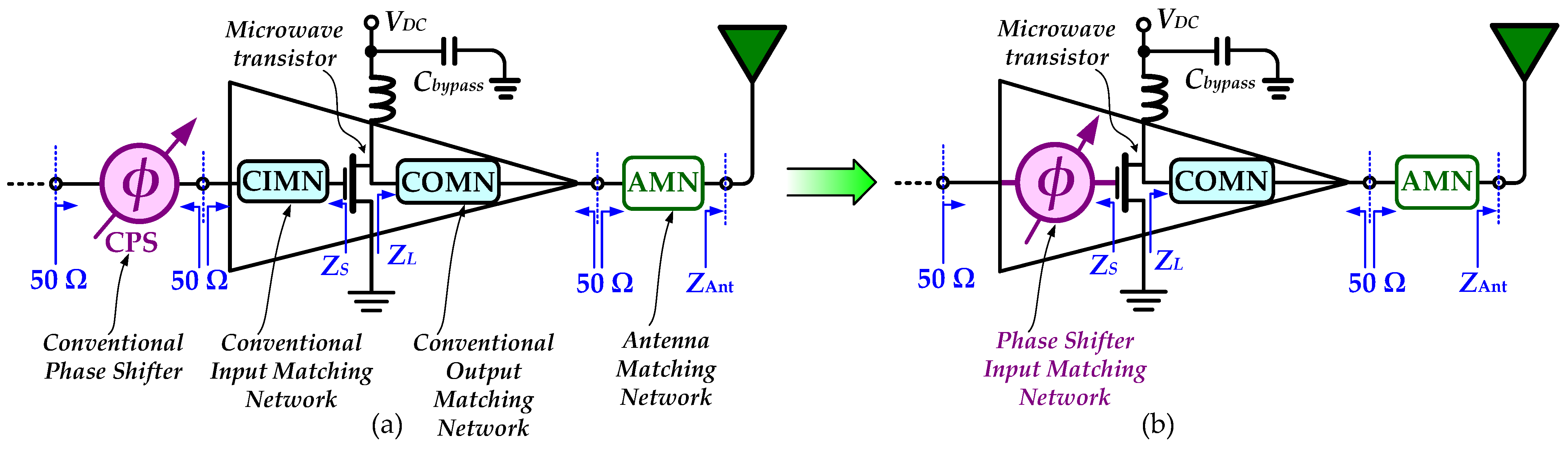
1. Introduction
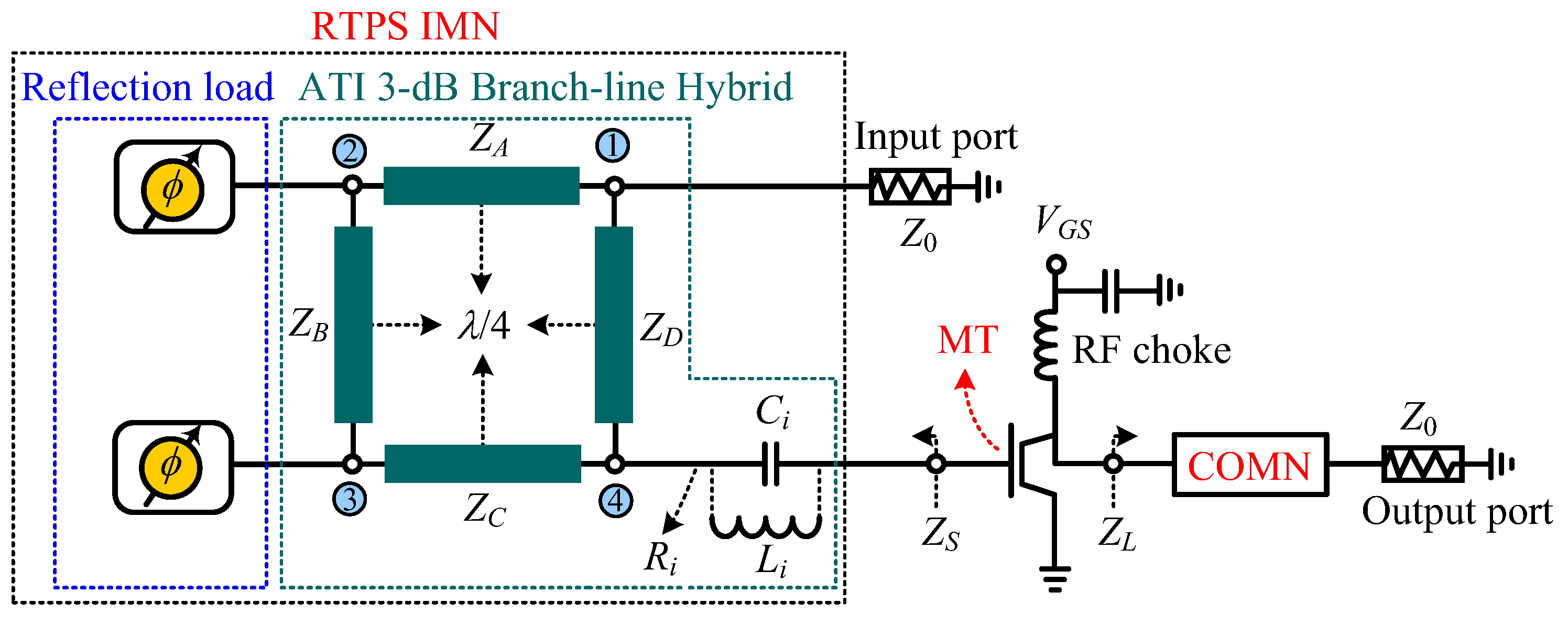
2. Design Method
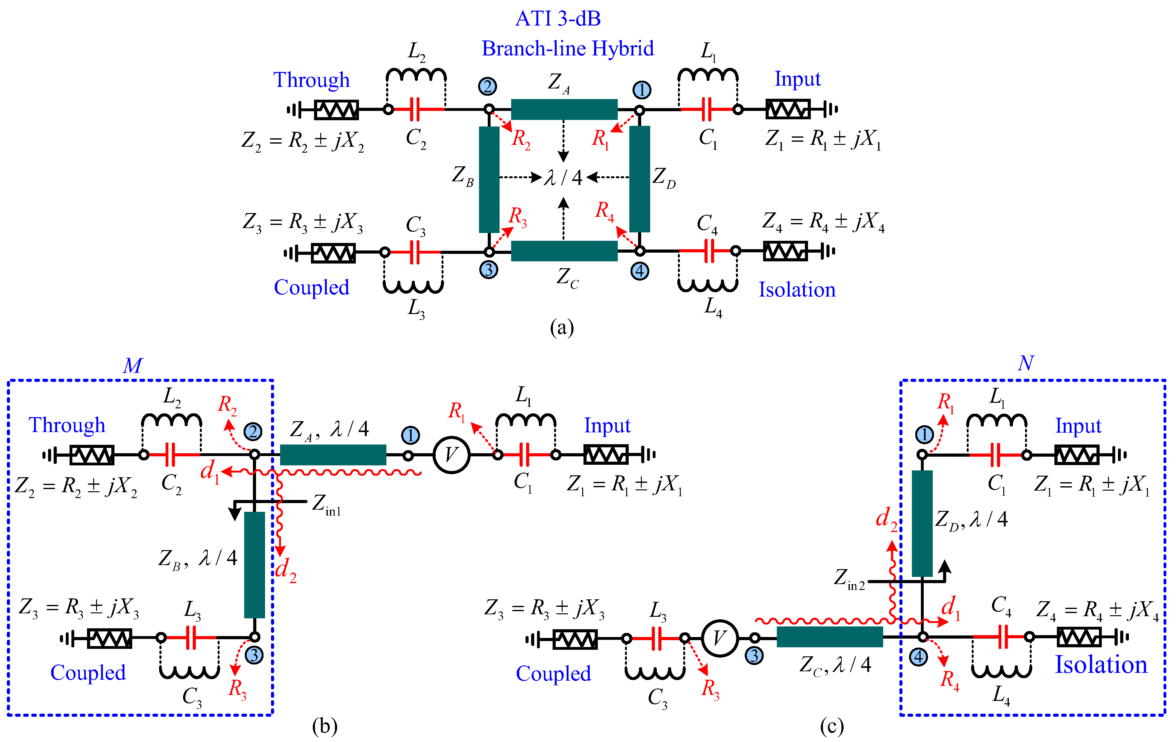
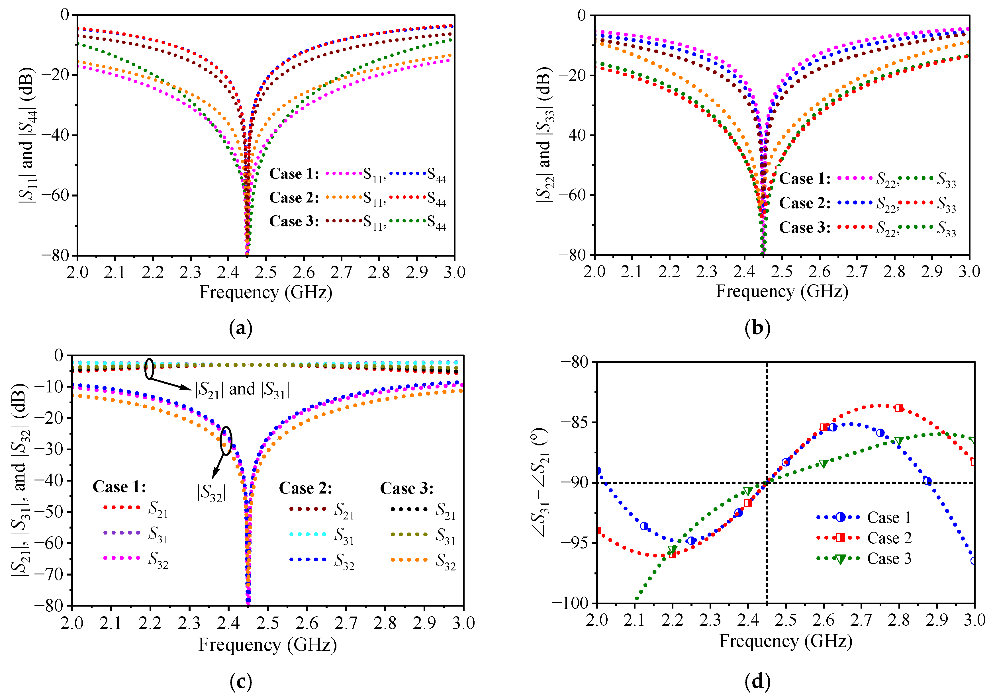
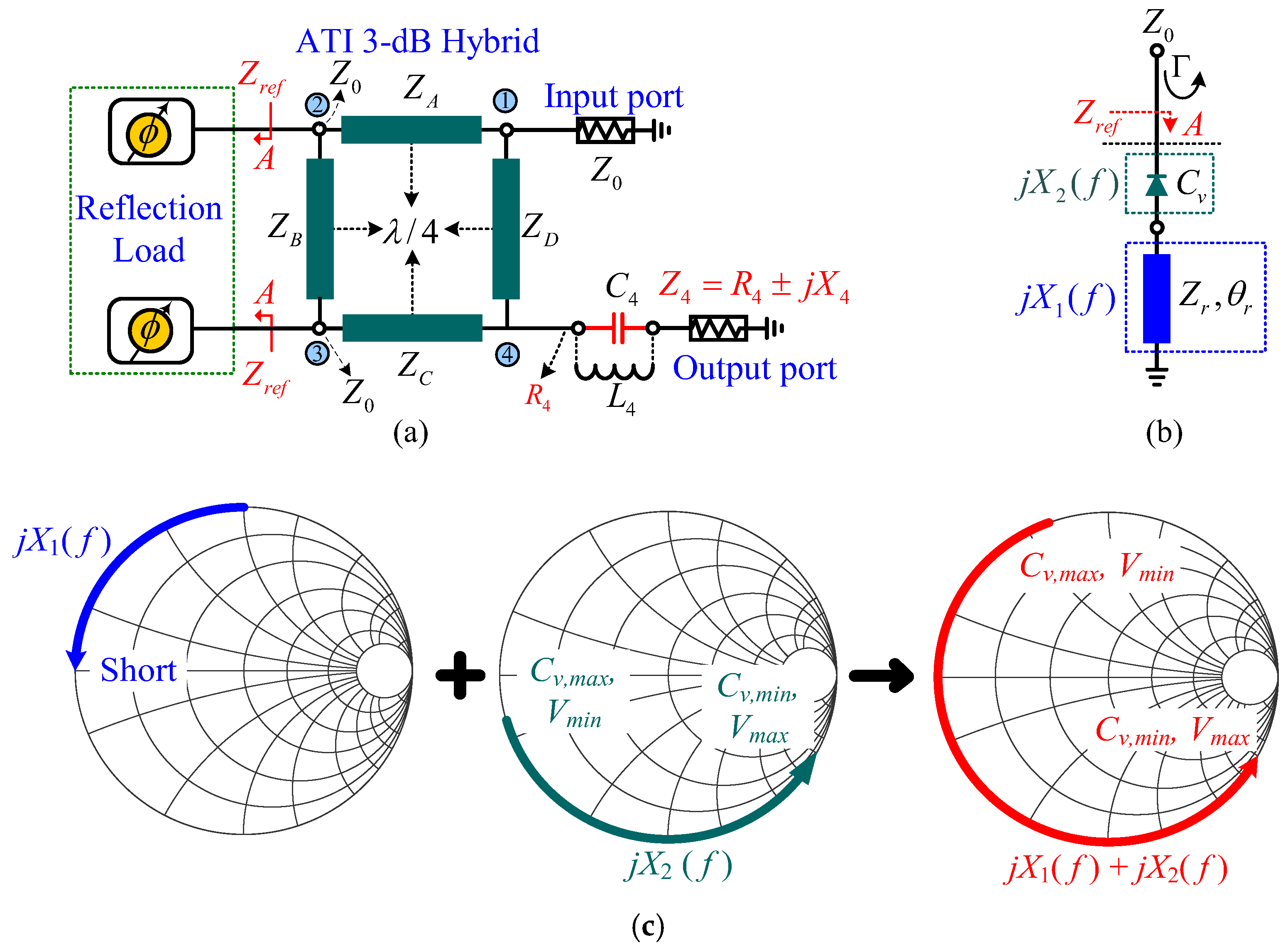
2.1. Arbitrary Termination Impedance 3 dB Branch–Line Hybrid
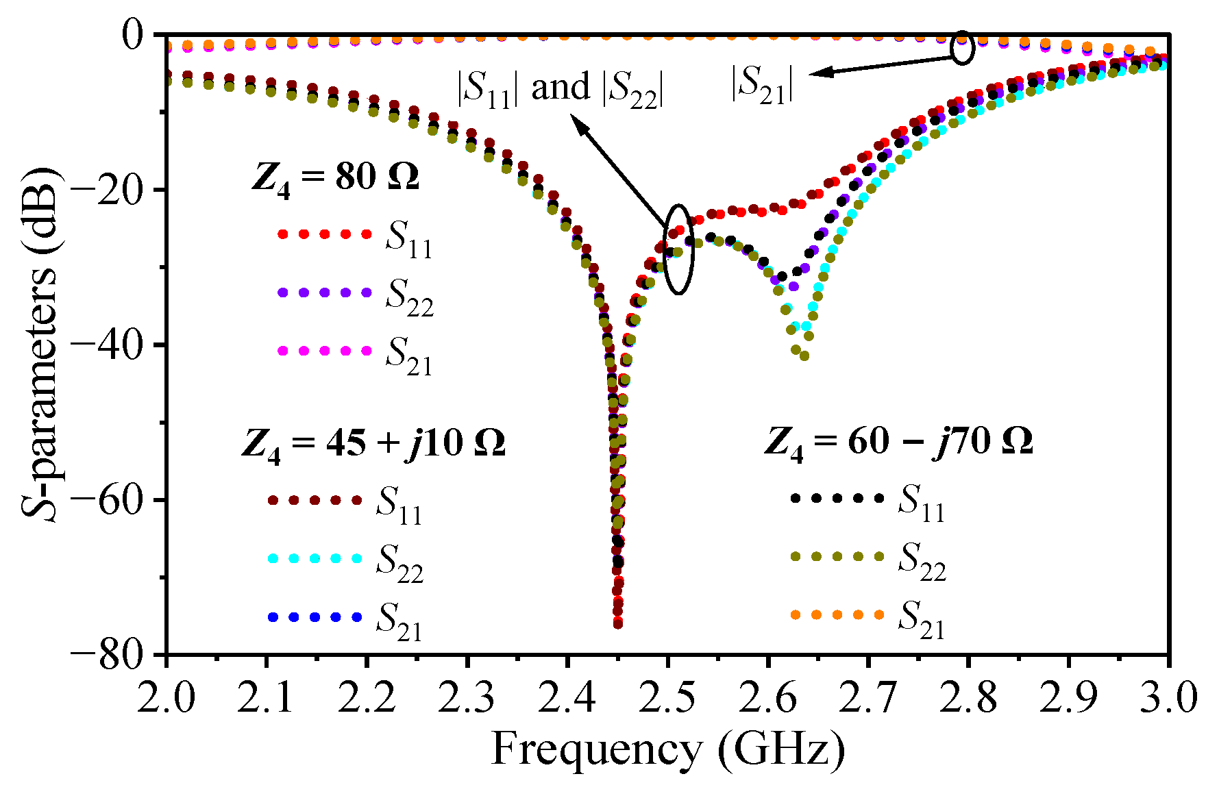
2.2. Arbitrary Termination Impedance Reflection-Type Phase Shifter
3. Experimental Results
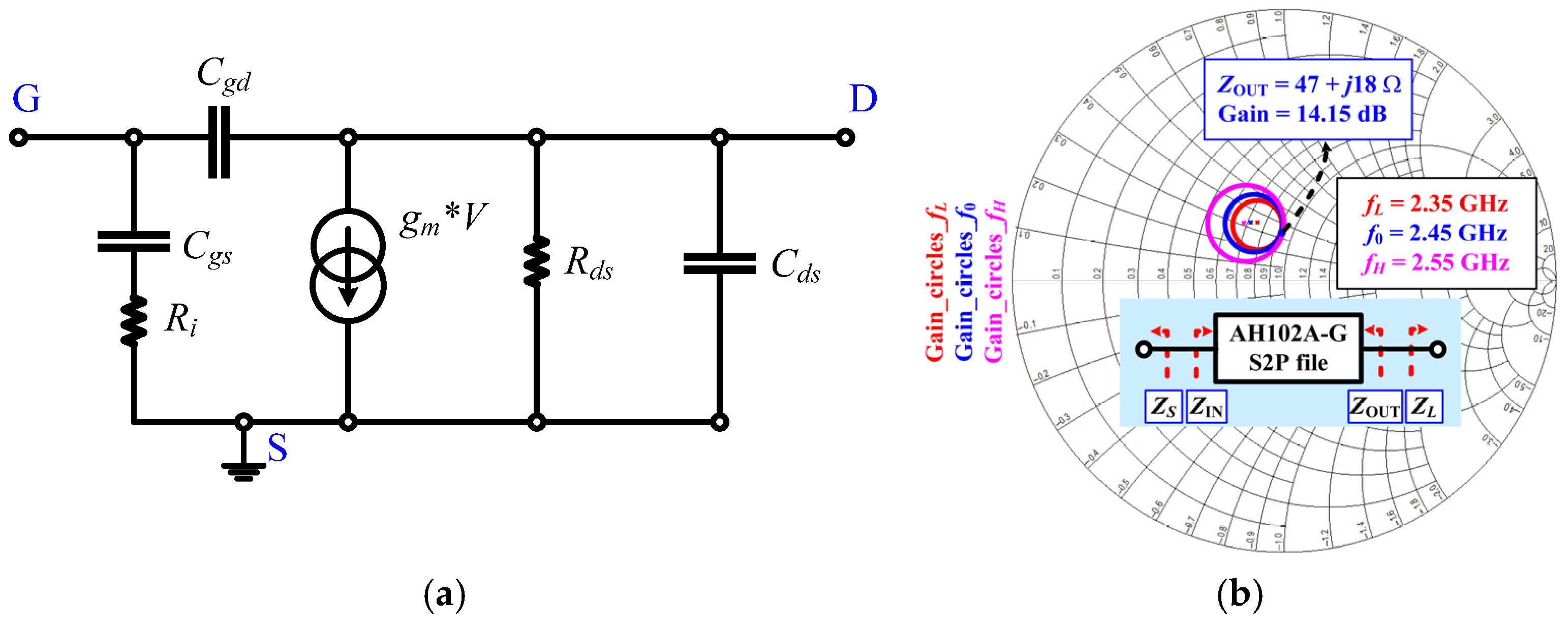
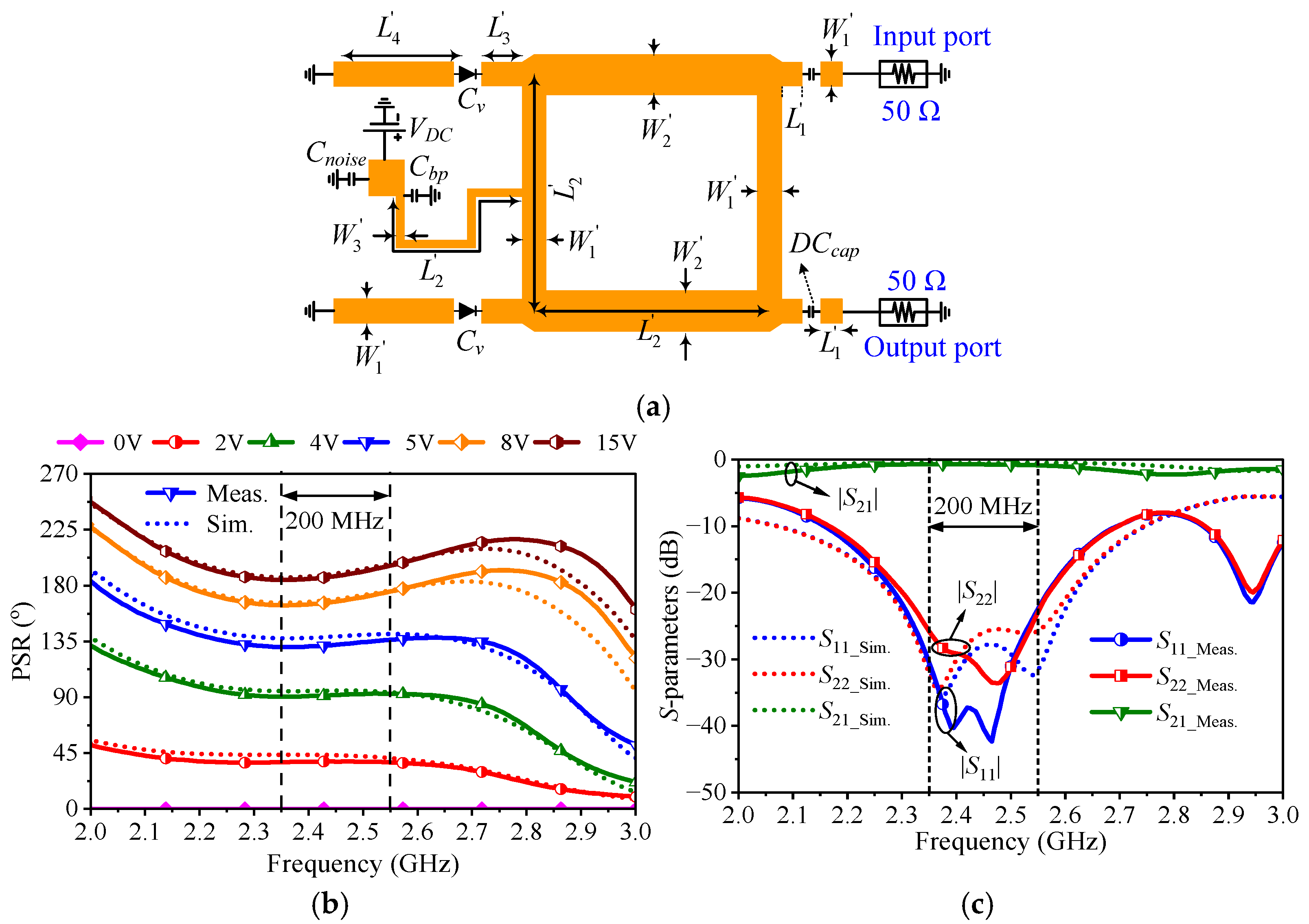
3.1. Conventional Cascaded Design of the Microwave Amplifier–Phase Shifter
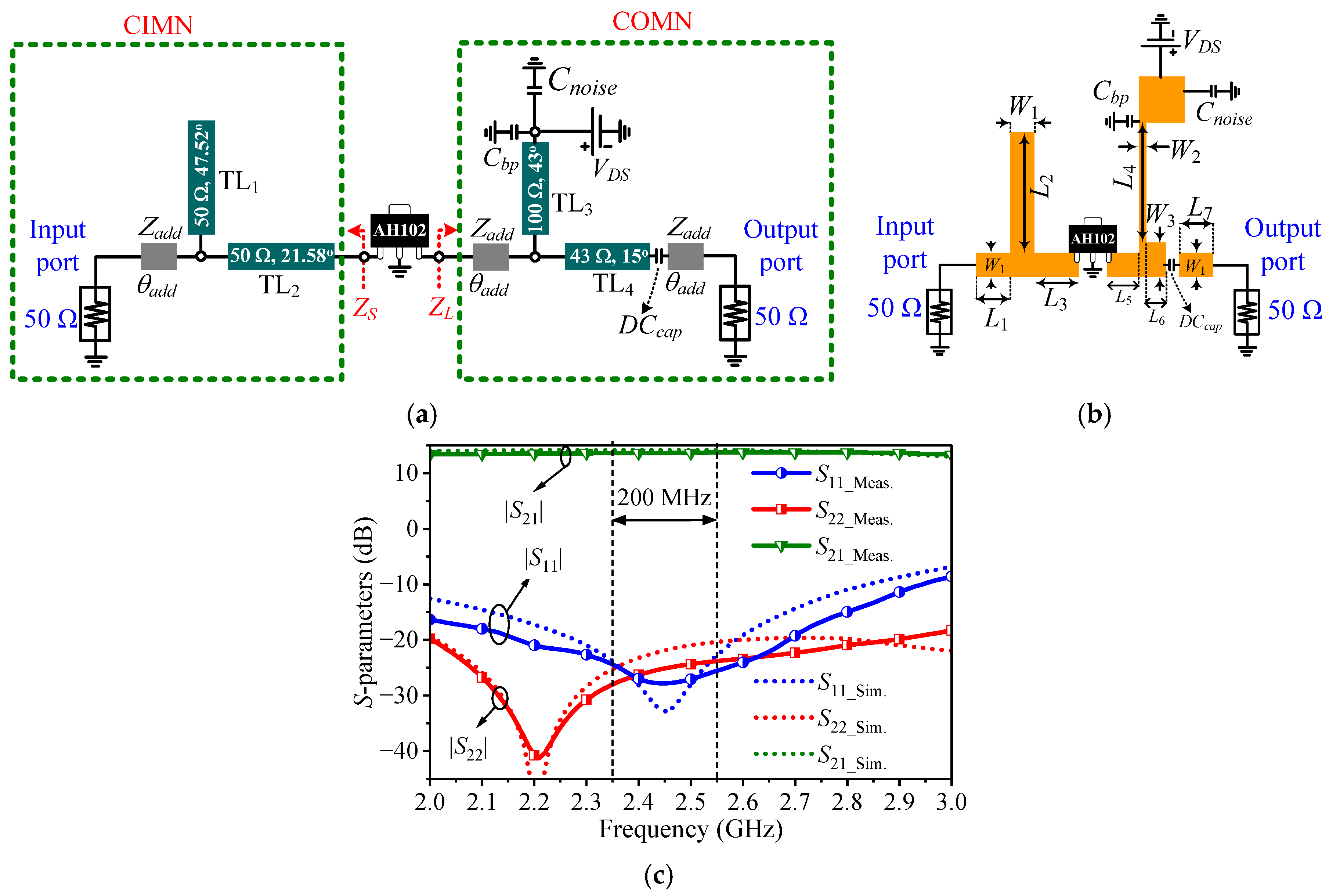
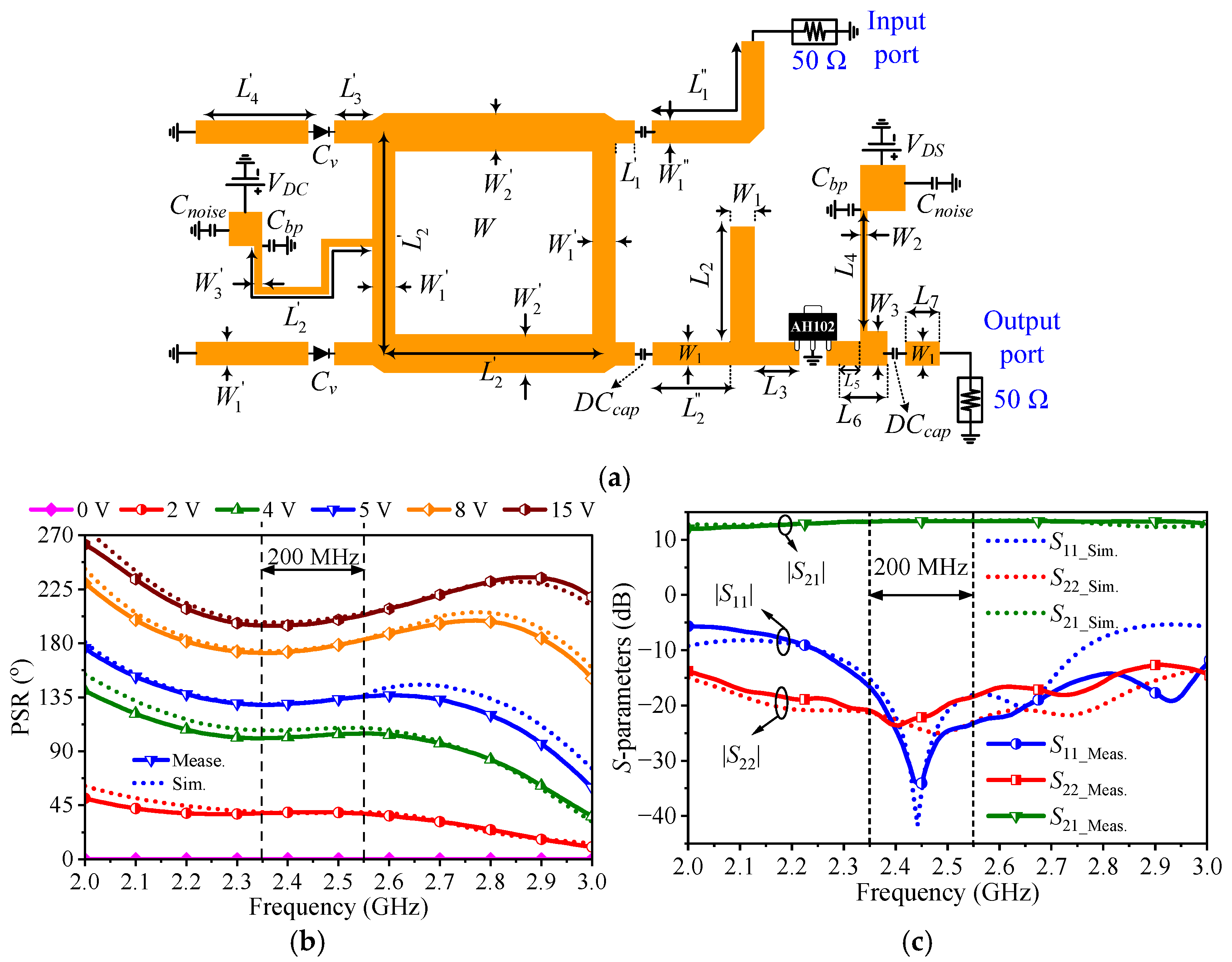
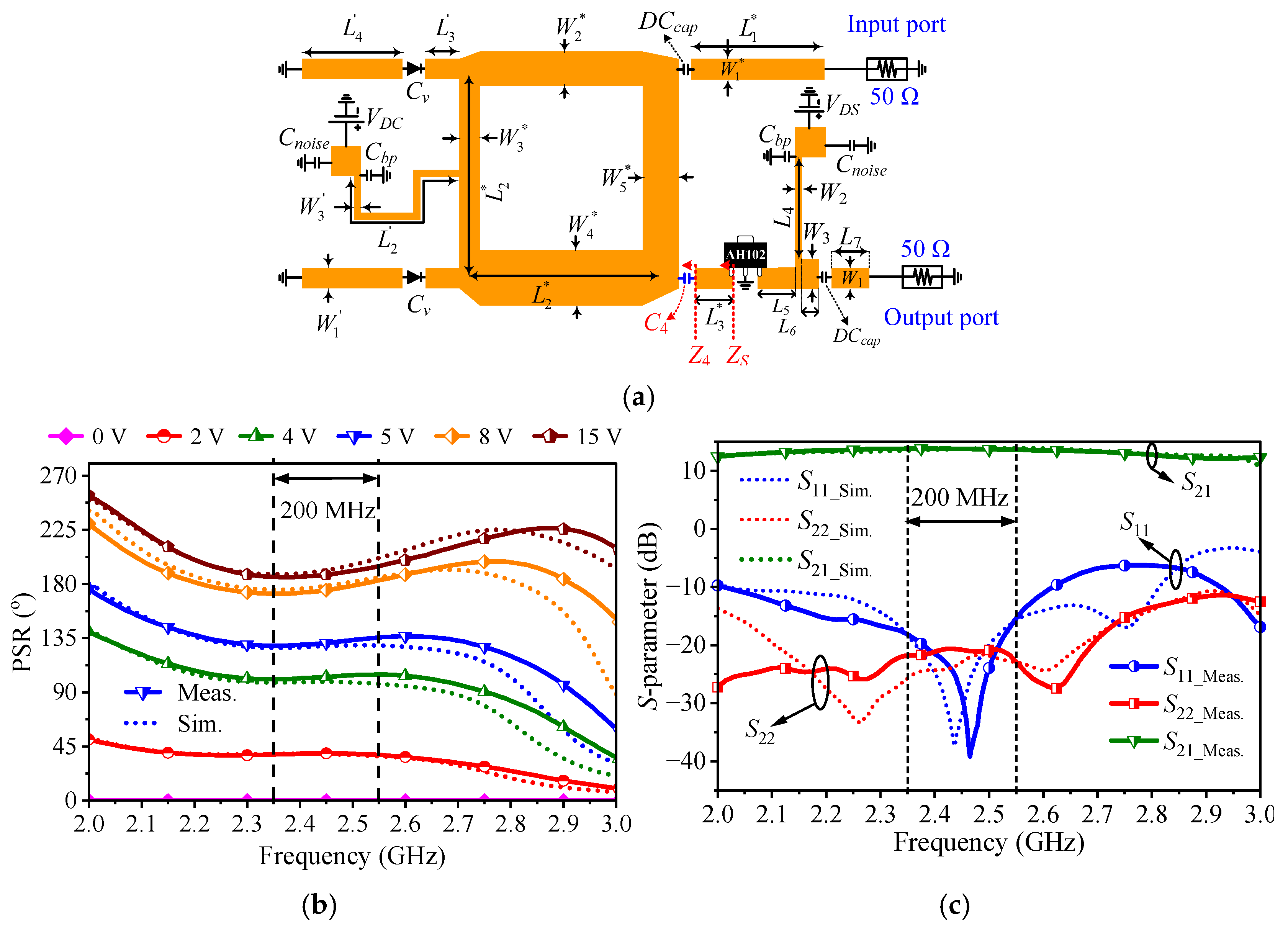
3.2. Co-Design of the Microwave Amplifier–Phase Shifter
3.3. Results Comparison
4. Conclusions
Author Contributions
Funding
Institutional Review Board Statement
Informed Consent Statement
Data Availability Statement
Conflicts of Interest
Abbreviations
| ADS | Advanced Design System |
| BW | Bandwidth |
| HFSS | High-Frequency Structure Simulator |
| IL | Insertion Loss |
| MIMO | Multiple Input and Multiple Output |
| RF | Radio Frequency |
| RL | Return Loss |
| TL | Transmission Line |
References
- Pech, P.; Kim, P.; Jeong, Y. Co-design of a low noise amplifier with compact substrate integrated waveguide bandpass filtering matching network. Int. J. RF Microw. Comput. Aided Eng. 2022, 32, e23498. [Google Scholar] [CrossRef]
- Su, Z.; Yu, C.; Tang, B.; Liu, Y. Bandpass filtering power amplifier with extended band and high efficiency. IEEE Microw. Wirel. Compon. Lett. 2020, 30, 181–184. [Google Scholar] [CrossRef]
- Chang, C.-H.; Chen, J.-Y.; Shen, C.-T.; Tsai, M.-J.; Tai, T.-S. Reflection-type phase shifter integrated with tunable power attenuation mechanism for sub-6 GHz wireless applications. IEEE Access. 2022, 10, 115532–115540. [Google Scholar] [CrossRef]
- Zheng, Z.Z.; Zhang, Y.-M.; Zheng, S.Y. A continuously tunable wideband differential phase shifter with filtering function and passband alignment. IEEE Trans. Microw. Theory Techno. 2025, 73, 620–630. [Google Scholar] [CrossRef]
- Zhang, Z.; Psychogiou, D. Multifunctional bandpass filter with codesigned tunable attenuator and reflectionless phase shifter functionalities. IEEE Microw. Wirel. Technol. Lett. 2024, 34, 737–740. [Google Scholar] [CrossRef]
- Lyu, Y.-P.; Zhu, L.; Cheng, C.-H. Proposal and synthesis design of differential phase shifters with filtering function. IEEE Trans. Microw. Theory Techn. 2017, 65, 2906–2917. [Google Scholar] [CrossRef]
- Moon, S.-M.; Yun, S.; Yom, I.-B.; Lee, H.L. Phase array shaped-beam satellite antenna with boosted-beam control. IEEE Trans. Antennas Propag. 2019, 67, 7633–7636. [Google Scholar] [CrossRef]
- Lee, W.-S.; Song, H.-K. Efficient channel feedback scheme for multi-user MIMO hybrid beamforming systems. Sensors 2021, 21, 5298. [Google Scholar] [CrossRef]
- Ayed, A.B.; Jaffri, I.; Darwish, A.M.; Mitran, P.; Boumaiza, S. Proof-of-concept of millimeter-wave RF beamforming transmitter architecture employing frequency-multiplier-based up-converters. IEEE Microw. Wirel. Compon. Lett. 2022, 32, 776–779. [Google Scholar] [CrossRef]
- Kim, S.; Park, H.; Min, B.-W. A center-fed beam-steerable series antenna array with a wide matching bandwidth. IEEE Open J. Antennas Propag. 2024, 5, 879–887. [Google Scholar] [CrossRef]
- Zheng, S.Y.; Chan, W.S.; Man, F.K. Broadband phase shifter using loaded transmission line. IEEE Microw. Wirel. Compon. Lett. 2010, 20, 498–500. [Google Scholar] [CrossRef]
- Gaun, C.-E.; Kanaya, H. 360° Phase shifter design using dual-branch switching network. IEEE Microw. Wirel. Compon. Lett. 2018, 28, 675–677. [Google Scholar] [CrossRef]
- Burdin, F.; Iskandar, Z.; Podevin, F.; Ferrari, P. Design of compact reflection-type phase shifters with high figure-of-merit. IEEE Trans. Microw. Theory Techn. 2015, 63, 1883–1893. [Google Scholar] [CrossRef]
- Yang, G.; Lee, D.; Min, B.-W. Low delay and loss variation reflection type phase shifter with sequentially controlled varactor diodes. In Proceedings of the 2023 IEEE/MTT-S International Microwave Symposium-IMS 2023, San Diego, CA, USA, 11–16 June 2023; pp. 1050–1053. [Google Scholar]
- Saron, S.; Chaudhary, G.; Jeong, Y. Concurrent dual-band shifter with independent tunable phase shift control. IEEE Microw. Wirel. Technol. Lett. 2024, 34, 163–166. [Google Scholar] [CrossRef]
- Liu, W.J.; Zheng, S.Y.; Pan, Y.M.; Li, Y.X.; Long, Y.L. A wideband tunable reflection-type phase shifter with wide relative phase shift. IEEE Trans. Circuits Syst. II Exp. Briefs. 2017, 64, 1442–1446. [Google Scholar] [CrossRef]
- An, B.; Chaudhary, G.; Jeong, Y. Wideband tunable phase shifter with low in-band phase deviation using coupled line. IEEE Microw. Wirel. Compon. Lett. 2018, 28, 678–680. [Google Scholar] [CrossRef]
- Chaudhary, G.; An, B.; Jeong, Y. In-band phase deviation minimization method for wideband tunable phase shifter. Microw. Opt. Technol. Lett. 2018, 61, 537–541. [Google Scholar] [CrossRef]
- Chaudhary, G.; Jeong, Y. Wideband tunable differential phase shifter with minimized in-band phase deviation error. IEEE Microw. Wirel. Compon. Lett. 2019, 29, 468–470. [Google Scholar] [CrossRef]
- Amin, F.; Liu, L.; Liu, Y.; Zhao, Y. Compact single-unit two-bit reflection-type phase shifters with large phase shift range. Electronics 2023, 12, 2412. [Google Scholar] [CrossRef]
- Singh, A.; Mandal, M.K. Electronically tunable reflection type phase shifters. IEEE Trans. Circuits Syst. II Exp. Briefs. 2020, 67, 425–429. [Google Scholar] [CrossRef]
- Zhu, H.; Abbosh, A.M. Wideband tunable reflection-type phase shifter using high-directivity directional coupler. In Proceedings of the 2018 Australian Microwave Symposium (AMS), Brisbane, Australia, 6–7 February 2018; pp. 49–50. [Google Scholar]
- Lyu, Y.-P.; Zhu, L.; Wang, S.-T.; Cheng, C.-H. A new synthesis method to design broadband continuously tunable phase shifters based on coupled line with low phase error. IEEE Trans. Microw. Theory Techn. 2025, 73, 2869–2878. [Google Scholar] [CrossRef]
- Ahn, H.-R. Asymmetric Branch-Line Hybrids in Asymmetric Passive Component in Microwave Integrated Circuits; Jonh Wiley & Sons, Inc.: Hoboken, NJ, USA, 2006; pp. 141–144. [Google Scholar]
- Kameche, M.; Feham, M.; Meliani, M.; Benahmed, N.; Dali, S. Intrinsic Small-Signal Equivalent Circuit of GaAs MESFET’s; National Centre of Space Techniques, AlgeriaTelecom Laboratory, University of Tlemcen: Tlemcen, Algeria, 2006. [Google Scholar]
- Pozar, D.M. Power dividers and directional coupler. In Microwave Engineering, 4th ed.; Jonh Wiley & Sons, Inc.: Hoboken, NJ, USA, 2012; pp. 343–346. [Google Scholar]


| Z1 [Ω] | Z2 [Ω] | Z3 [Ω] | Z4 [Ω] | Ci [pF] or Li [nH] (i = 1~4) | ZA [Ω] | ZB [Ω] | ZC [Ω] | ZD [Ω] | |
|---|---|---|---|---|---|---|---|---|---|
| Case 1 | 20 | 50 | 30 | 80 | 0/0/0/0 | 22.36 | 38.73 | 34.64 | 40 |
| Case 2 | 25 | 50 − j60 | 40 + j20 | 120 | 0/3.9 nH/3.25 pF/0 | 25 | 44.72 | 48.99 | 54.73 |
| Case 3 | 35 − j40 | 30 + j125 | 75 − j60 | 45 + j10 | 2.6 nH/0.52 pF/3.9 nH/6.5 pF | 22.91 | 47.43 | 41.08 | 39.69 |
| Z1, Z2, Z3 | Z4 | C4/ L4 | ZA | ZB | ZC | ZD | Zr | θr (°) | PSR (°) | PDE (°) |
|---|---|---|---|---|---|---|---|---|---|---|
| 50 | 80 | 0 | 35.36 | 50 | 44.72 | 63.25 | 30/50/80 | 30/45/60 | 157.8/214.5/233.2 | 3.8/7.4/39.8 |
| 50 | 45 + j10 | C4 = 6.5 pF | 35.36 | 50 | 33.54 | 47.43 | 30/50/80 | 30/45/60 | 157.8/214.5/233.2 | 3.8/7.4/39.8 |
| 50 | 60 − j70 | L4 = 4.55 nH | 35.36 | 50 | 38.73 | 54.77 | 30/50/80 | 30/45/60 | 157.8/214.5/233.2 | 3.8/7.4/39.8 |
| Target | Part Number of Used Capacitors | Measured Capacitances at 2.45 GHz |
|---|---|---|
| Cnoise = 0.1 pF | VJ0603D0R1VXPAJ | Cnoise_meas. = 0.13 pF |
| Cbp = 33 pF | 0603N8R2AW251 | Cbp_meas. = 32.92 pF |
| DCcap = 20 pF | 0603N5R6AW251 | DCcap_meas. = 20.1 pF |
| C4 = 4.87 pF | 0603N3R3AW251 | C4_meas. = 4.9 pF |
| MAs | Gain (dB) | P1dB (dBm) | PSR (°) | PDE (°) | Size |
|---|---|---|---|---|---|
| CMA | 14.13 | 25.72 | – | – | 0.42 λ0 × 0.37 λ0 |
| CRTPS cascaded with CMA | 13.28 | 24.77 | 195.35 | ±6.14 | 1.06 λ0 × 0.47 λ0 |
| Proposed co-design MA-PS | 13.74 | 25.26 | 185.62 | ±4.3 | 0.74 λ0 × 0.50 λ0 |
| 201.17 | ±6.14 |
Disclaimer/Publisher’s Note: The statements, opinions and data contained in all publications are solely those of the individual author(s) and contributor(s) and not of MDPI and/or the editor(s). MDPI and/or the editor(s) disclaim responsibility for any injury to people or property resulting from any ideas, methods, instructions or products referred to in the content. |
© 2025 by the authors. Licensee MDPI, Basel, Switzerland. This article is an open access article distributed under the terms and conditions of the Creative Commons Attribution (CC BY) license (https://creativecommons.org/licenses/by/4.0/).
Share and Cite
Thorng, P.; Pech, P.; Chaudhary, G.; Jeong, Y. Co-Design of Integrated Microwave Amplifier and Phase Shifter Using Reflection-Type Input Matching Networks for Compact MIMO Systems. Appl. Sci. 2025, 15, 7539. https://doi.org/10.3390/app15137539
Thorng P, Pech P, Chaudhary G, Jeong Y. Co-Design of Integrated Microwave Amplifier and Phase Shifter Using Reflection-Type Input Matching Networks for Compact MIMO Systems. Applied Sciences. 2025; 15(13):7539. https://doi.org/10.3390/app15137539
Chicago/Turabian StyleThorng, Palaystint, Phanam Pech, Girdhari Chaudhary, and Yongchae Jeong. 2025. "Co-Design of Integrated Microwave Amplifier and Phase Shifter Using Reflection-Type Input Matching Networks for Compact MIMO Systems" Applied Sciences 15, no. 13: 7539. https://doi.org/10.3390/app15137539
APA StyleThorng, P., Pech, P., Chaudhary, G., & Jeong, Y. (2025). Co-Design of Integrated Microwave Amplifier and Phase Shifter Using Reflection-Type Input Matching Networks for Compact MIMO Systems. Applied Sciences, 15(13), 7539. https://doi.org/10.3390/app15137539