Review

Integrated Photonics for IoT, RoF, and Distributed Fog–Cloud Computing: A Comprehensive Review

by
Gerardo Antonio Castañón Ávila
1,*,
Walter Cerroni
2 and
Ana Maria Sarmiento-Moncada
1
1
School of Engineering and Science, Tecnologico de Monterrey, Ave. Eugenio Garza Sada 2501, Monterrey 64849, Mexico
2
Department of Electrical, Electronic and Information Engineering “G. Marconi”, University of Bologna, 40136 Bologna, Italy
*
Author to whom correspondence should be addressed.
Appl. Sci. 2025, 15(13), 7494; https://doi.org/10.3390/app15137494
Submission received: 8 May 2025 / Revised: 16 June 2025 / Accepted: 24 June 2025 / Published: 3 July 2025
(This article belongs to the Special Issue New Trends in Next-Generation Optical Networks)

Abstract

Integrated photonics is a transformative technology for enhancing communication and computation in Cloud and Fog computing networks. Photonic integrated circuits (PICs) enable significant improvements in data-processing speed, energy-efficiency, scalability, and latency. In Cloud infrastructures, PICs support high-speed optical interconnects, energy-efficient switching, and compact wavelength division multiplexing (WDM), addressing growing data demands. Fog computing, with its edge-focused processing and analytics, benefits from the compactness and low latency of integrated photonics for real-time signal processing, sensing, and secure data transmission near IoT devices. PICs also facilitate the low-loss, high-speed modulation, transmission, and detection of RF signals in scalable Radio-over-Fiber (RoF) links, enabling seamless IoT integration with Cloud and Fog networks. This results in centralized processing, reduced latency, and efficient bandwidth use across distributed infrastructures. Overall, integrating photonic technologies into RoF, Fog and Cloud computing networks paves the way for ultra-efficient, flexible, and scalable next-generation network architectures capable of supporting diverse real-time and high-bandwidth applications. This paper provides a comprehensive review of the current state and emerging trends in integrated photonics for IoT sensors, RoF, Fog and Cloud computing systems. It also outlines open research opportunities in photonic devices and system-level integration, aimed at advancing performance, energy-efficiency, and scalability in next-generation distributed computing networks.

1. Introduction

The rapid expansion of data-intensive applications such as artificial intelligence (AI), machine learning (ML), and the Internet of Things (IoT) has significantly increased demands on Cloud and Fog computing infrastructures. Traditional electronic interconnects are encountering fundamental limitations, including bandwidth bottlenecks, increased latency, and inefficient energy utilization. Integrated photonics, which involves integrating multiple photonic components—lasers, modulators, detectors, and waveguides—onto a single chip, has emerged as a promising approach to overcome these challenges by enabling high-speed, low-energy optical data transmission [1,2].
In Cloud computing networks, integrated photonics is transforming data center interconnectivity by achieving ultra-high bandwidth and greatly reduced energy consumption. Recent advances in photonic integrated circuits (PICs) demonstrate the potential to perform high-speed analog signal processing tasks with higher efficiency than conventional electronic solutions, significantly enhancing data handling capabilities in modern data centers [1]. Companies such as Intel and Nvidia are actively integrating optical input/output technologies directly onto processors and network switches, pushing interconnect speeds to terabit-per-second scales, which are essential for AI-driven workloads [3,4].
Similarly, Fog computing networks, which extend Cloud functionality toward the network edge, stand to benefit substantially from integrated photonics. The compact size, energy-efficiency, and low latency characteristics of PICs make them ideally suited for deployment in edge devices, where real-time data analysis and rapid decision-making are crucial. Recent developments have illustrated the viability of photonic processors for executing complex edge computing tasks, such as real-time digital image convolution, achieving substantial gains in processing speed and energy-efficiency compared to traditional electronic processors [5].
The migration of telecommunication companies to photonic integrated CMOS-based technologies for components utilized in Fog and Cloud computing is driven by critical advantages such as low power consumption, high integration density, scalability, and cost efficiency. CMOS technology offers unparalleled miniaturization and energy-efficiency, which are essential for Fog computing nodes that require processing capabilities at the edge with minimal power budgets and compact footprints [6]. Additionally, the scalability of CMOS fabrication processes aligns perfectly with the growing demand for Cloud-based data centers where high-density integration significantly reduces operational costs and enhances system reliability [7]. The compatibility of CMOS with advanced semiconductor processes also ensures continuous performance improvements through technology scaling, making it the ideal choice for future-proofing the computing infrastructure required for Fog and Cloud paradigms [8].
PICs have become key enablers in modern Radio-over-Fiber (RoF) systems, offering compact, energy-efficient, and scalable solutions for high-frequency signal transport over optical fiber. PIC-based RoF systems integrate essential components such as modulators, photodetectors, multiplexers, and amplifiers onto a single chip, significantly reducing footprint, power consumption, and complexity compared to traditional discrete implementations [9,10]. These integrated platforms support wide bandwidths and low-loss signal propagation, which are critical for transporting millimeter-wave and 5G signals in dense IoT environments [10]. In addition, RoF systems enabled by PICs facilitate seamless interconnection between IoT devices, Fog nodes, and Cloud data centers by centralizing signal processing functions while ensuring low-latency, high-fidelity transmission [11]. The work of Castanon et al. [12,13] has demonstrated the feasibility and performance advantages of integrated RoF architectures for broadband access and 5G fronthaul, highlighting the impact of PICs in next-generation network infrastructures. As silicon photonics and heterogeneous integration continue to evolve, PIC-enabled RoF systems are poised to play a central role in the deployment of cost-effective, high-capacity, and flexible access networks.
This review paper presents a comprehensive analysis of the emerging role of PIC technology in the evolution of next-generation sensing and computing infrastructures. Specifically, it highlights the transformative potential of PICs in enhancing the performance, scalability, and energy-efficiency of Internet of Things (IoT) sensor networks, Fog computing architectures, and Cloud-based data-processing systems. By synthesizing recent advancements in integrated photonics, the review identifies how PIC-based solutions enable high-speed, low-latency data transmission and processing at the edge (Fog) and core (Cloud) layers, while reducing the size, cost, and power consumption of sensor nodes. Furthermore, the paper outlines the current challenges and future research directions required to fully integrate PICs into distributed intelligent systems, ultimately contributing to the realization of faster, smarter, and more sustainable digital infrastructures.
Despite these promising advancements, several challenges persist, such as the need for standardized fabrication processes, effective integration with existing electronic systems, and overcoming scalability constraints in manufacturing. Continued research and industry collaboration are therefore vital for addressing these barriers and fully realizing the transformative potential of integrated photonics in both Cloud and Fog computing networks [14,15].
To ensure comprehensive coverage, a systematic literature review was conducted. following the PRISMA (Preferred Reporting Items for Systematic Reviews and Meta-Analyses) methodology as a guiding framework. Relevant studies were identified using major scientific databases, including IEEE Xplore, ScienceDirect, and Scopus, focusing on publications from 2012 to 2025. The search strategy employed targeted keywords such as “integrated photonics”, “Fog computing”, “cloud datacenters”, “photonic integrated circuits”, “radio over fiber”, and “IoT sensors”. Inclusion criteria were limited to peer-reviewed journal articles and high-impact conference proceedings directly relevant to photonic integration in distributed computing environments. Although not all PRISMA items were strictly applied, the review process adhered to its core principles to ensure transparency, relevance, and rigor in the selection and synthesis of sources.
The remainder of this paper is structured as follows: Section 2 describes the hierarchical architecture of IoT, Fog, and Cloud computing. Section 3 presents the role of Radio-over-Fiber (RoF) in enabling IoT and Fog computing. Section 4 summarizes key Fog computing application scenarios. Section 5 discusses PIC-enabled IoT sensors. Section 6 reviews high-speed network technology enablers. Section 7 highlights current industry implementations. Section 8 outlines future trends and research directions. Section 9 outlines a summary of benefits and Section 10 discusses the implementation challenges and emerging solutions. Finally, Section 11 provides the conclusions.

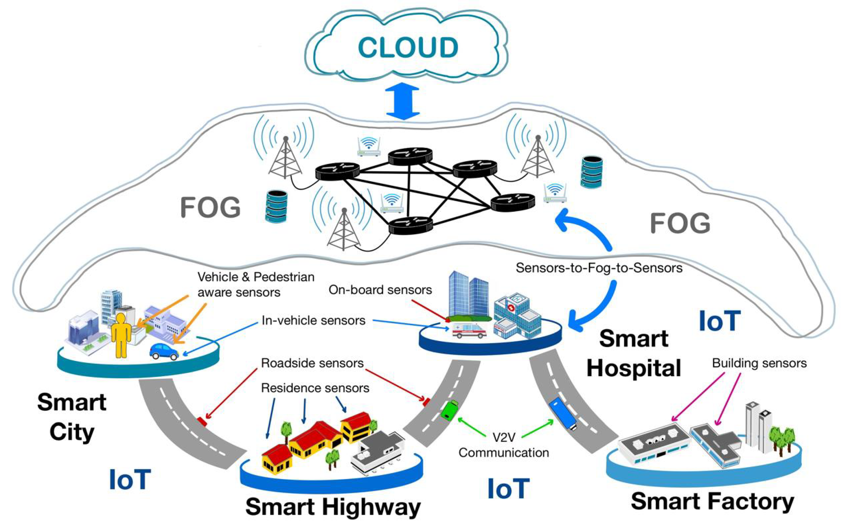
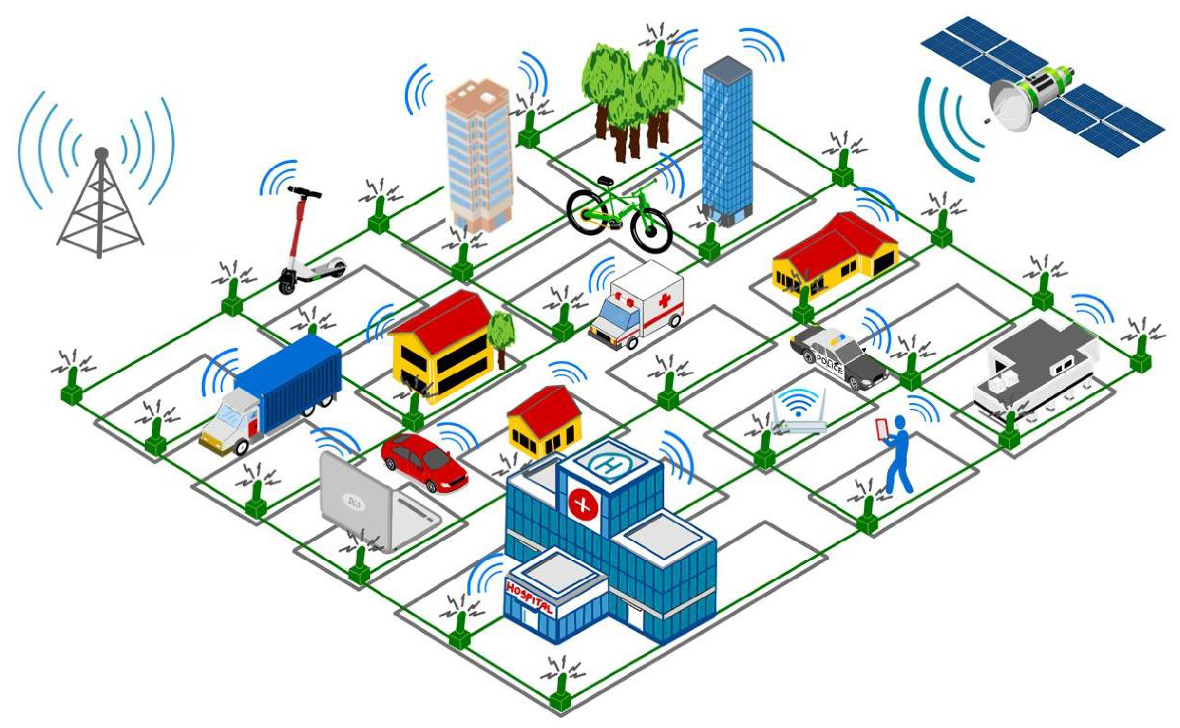
2. Hierarchical IoT, Fog/Cloud Computing Architecture

Figure 1 illustrates the hierarchical architecture of an integrated IoT, RoF, Fog, and Cloud computing system. This architecture is composed of three distinct yet interdependent layers, each fulfilling a specific role in the collection, processing, and management of data. At the base is the IoT layer, which includes a wide array of distributed sensing and actuating devices operating in diverse environments. These devices are responsible for real-time data acquisition and control, and serve as the interface between the physical and digital worlds. Above this, the Fog layer acts as an intermediate processing stage located near the edge of the network. It comprises gateways, routers, and localized servers that enable low-latency processing, temporary storage, and timely service delivery. Finally, the Cloud layer represents the centralized data-processing infrastructure, consisting of powerful data centers capable of performing intensive analytics, long-term storage, and resource scaling on demand. Radio-over-Fiber (RoF) technology plays a critical role in this architecture by enabling the transparent, low-latency transmission of high-frequency wireless signals over optical fiber, effectively bridging IoT endpoints with Fog nodes and Cloud infrastructure when needed. By using RoF links, wireless access points and distributed sensors can be interconnected with centralized processing resources while preserving high bandwidth and real-time responsiveness. Together, these layers—interconnected through RoF—form a cohesive and efficient architecture for supporting intelligent, distributed applications in next-generation digital ecosystems.
Table 1 compares Fog and Cloud computing across several key system requirements, highlighting their complementary roles in distributed computing infrastructures. Fog computing prioritizes ultra-low-latency, energy-efficiency, and real-time responsiveness at the network edge—features critical for time-sensitive applications such as industrial automation, autonomous systems, and IoT deployments. In contrast, Cloud computing excels in centralized scalability, high-capacity data-processing, and long-term storage, making it ideal for tasks such as big data analytics and machine learning training. The table also illustrates how communication requirements differ: Fog architectures rely more on wireless and geographically distributed links, whereas Cloud infrastructures are built on high-throughput fiber optic interconnections within and between data centers. Together, these paradigms enable a hierarchical computing model that balances proximity, performance, and scalability.

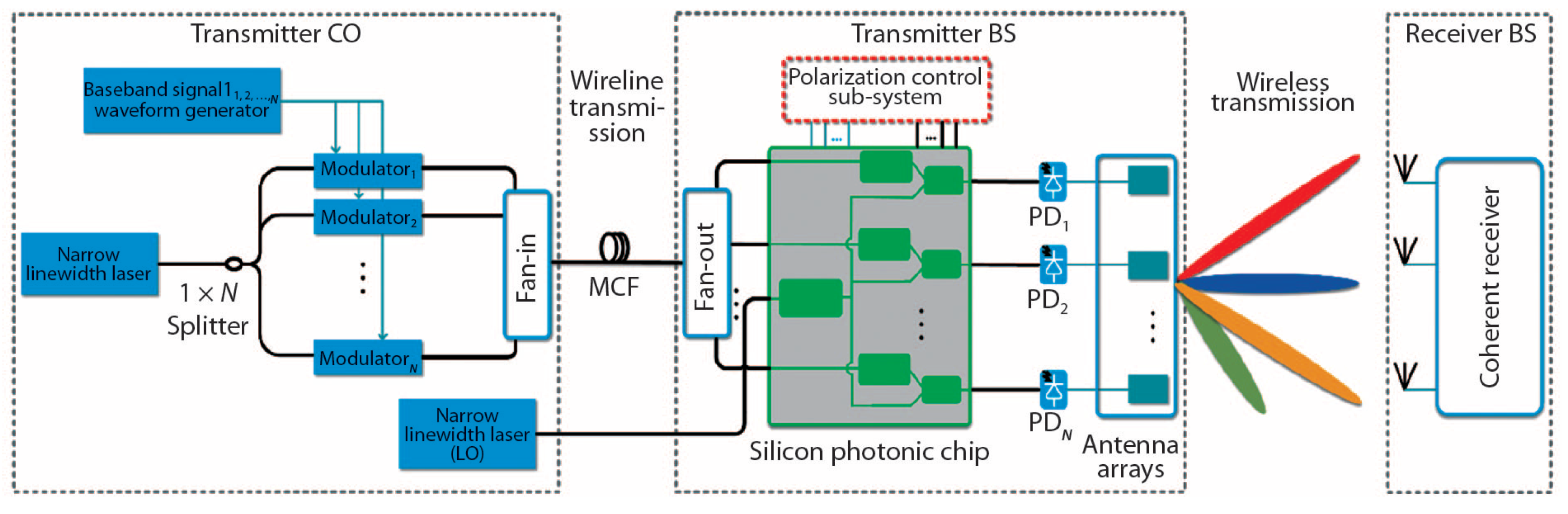
3. Radio-over-Fiber (RoF) for IoT and Fog Computing

Radio-over-Fiber (RoF), shown in Figure 2, is a technology that enables the transmission of radio frequency (RF) signals over optical fiber links, combining the low-loss, high-bandwidth characteristics of fiber optics with the flexibility and ubiquity of wireless communication [9,10,16]. Unlike traditional coaxial cables or free-space transmission, RoF allows RF signals to be centrally generated, modulated, and distributed over long distances with minimal signal degradation. This capability makes RoF particularly attractive for emerging applications in IoT and Fog computing architectures.
In IoT systems, RoF provides an efficient backhaul and fronthaul infrastructure for dense deployments of wireless sensors and devices. It supports low-latency data transport from distributed IoT nodes—such as sensors, meters, and cameras—to Fog gateways and Cloud processing units, enabling real-time monitoring and control [12,16]. RoF also facilitates the aggregation of RF signals from heterogeneous low-power protocols (e.g., Bluetooth, LoRa, WiFi, 5G, and emerging 6G) and carries them via high-capacity optical fibers to centralized processing centers [13]. Moreover, RoF supports scalable deployment models such as centralized radio access networks, which reduce infrastructure complexity and maintenance overhead in smart city and industrial IoT environments [11]. Its ability to transport millimeter-wave and 5G signals over fiber with minimal loss further strengthens its relevance for next-generation wireless systems. For example, Moon et al. [17] proposed a hybrid RoF transport system to support heterogeneous indoor mobile networks, including 5G and 6G. Their approach enables the seamless integration of multiple wireless technologies over a unified optical infrastructure. NEC researchers also demonstrated a 1-bit outphasing modulation RoF system that delivers high bandwidth efficiency and complies with 3GPP standards, offering a cost-effective solution for indoor 5G/6G deployments [18]. These developments highlight RoF’s strong potential for unifying diverse wireless signals on a shared optical platform.
For Fog computing, which brings data storage, processing, and decision-making closer to the network edge, RoF offers several advantages. It enables high-speed, low-latency connections between edge devices and Fog nodes through fiber links, supporting real-time analytics and local actuation. The use of remote radio heads and centralized signal processing reduces the power and processing burden at edge nodes, making the architecture more energy-efficient and suitable for constrained environments [10]. Additionally, RoF allows for the dynamic allocation of wireless resources and centralized control of modulation and frequency schemes, enhancing the flexibility of Fog-based networks [19].
An illustrative example is a smart factory equipped with thousands of wireless sensors measuring variables such as temperature and vibration. Instead of embedding local processing in each sensor, lightweight RF-capable transceivers transmit signals to distributed access points. These RF signals are then carried over optical fiber using Radio-over-Fiber (RoF) links to a centralized fog node. This intermediate node performs real-time analytics on the incoming data and forwards summarized insights to the cloud for long-term storage or machine learning model updates [20].
Another illustrative example is a smart city environment equipped with thousands of distributed wireless sensors monitoring environmental conditions such as air quality, traffic flow, noise levels, energy consumption, and public safety parameters. Instead of relying on local processing at each sensor node—which would significantly increase power consumption and system complexity—lightweight transceivers transmit RF signals to strategically placed access points. These RF signals are then carried over optical fiber using RoF links to geographically distributed Fog nodes located in traffic management centers, utility hubs, or public safety stations. The Fog nodes perform real-time analytics to support immediate decision-making, such as dynamic traffic light control, air quality alerts, or emergency response coordination. Processed data and long-term trends are subsequently forwarded to Cloud servers for historical analysis, city-wide optimization, and predictive modeling. This RoF-enabled architecture ensures high-bandwidth, low-latency communication across the smart city while maintaining centralized control and scalability [21].
Overall, the integration of RoF with photonic technologies provides a scalable and energy-efficient foundation for future distributed computing networks, enabling seamless communication between IoT devices, Fog nodes, and Cloud infrastructures. Table 2 outlines key research opportunities for enhancing RoF systems through the integration of PICs [22,23]. It highlights how PICs can address specific figures of merit across cost, performance, scalability, and reliability in various RoF configurations.
Figure 3 presents a schematic of the experimental setup for generating multi-channel 28 GHz millimeter-wave signals using a silicon photonic integrated circuit. The system employs two tunable laser sources (TLSs) with orthogonal polarization states, which are aligned using a polarization controller (PC) and separated by a polarization beam-splitter (PBS). Each optical carrier is modulated independently by a Mach–Zehnder modulator (MZM) before being combined on-chip by a polarization beam combiner (PBC) implemented in silicon photonics. The polarization multiplexed signal is then converted into an electrical millimeter-wave output via a photodetector (PD). This configuration enables the compact and efficient integration of polarization control and high-frequency signal generation on a single chip [24].

4. Photonic Implementations in Fog Computing Domains

Integrated photonics has begun to shape the deployment of Fog computing across various domains where real-time processing, energy-efficiency, and scalability are essential. This section reorganizes key application areas by domain to emphasize real-world deployment contexts and highlight how photonic technologies enable these systems.

4.1. Smart Cities and Urban Infrastructure

Smart cities face numerous challenges, such as traffic congestion, public safety, energy management, sanitation, and internet connectivity [21,22,23]. Fog computing addresses these by enabling localized processing and storage near end devices, reducing reliance on centralized Cloud infrastructure. Key applications include smart parking, smart hospitals, smart healthcare systems, smart transportation, optimized highway usage, smart buildings, and software-defined factories. While cellular networks provide city-wide coverage, their limited capacity often falls short of supporting advanced city services. Integrating Fog computing with Bluetooth, LoRa, WiFi, 5G, and 6G technologies enables a scalable and responsive smart city infrastructure to be developed by offloading workloads to nearby Fog nodes and optimizing bandwidth utilization. Integrated photonic links further support high-speed, low-latency data transfer across urban sensor networks.
Example: Photonic-enabled high-speed fiber backhaul is increasingly being adopted for Roadside Units (RSUs) in intelligent transportation and urban IoT deployments to ensure low-latency and reliable communications over metropolitan-scale networks [25]. Meanwhile, Microsoft’s Project Silica explores durable, volumetric photonic storage using femtosecond laser-writing in quartz glass—promising archival data densities of several terabytes in DVD-sized volumes with lifespans measured in millennia [26].

4.2. Transportation and Autonomous Systems

Autonomous vehicles, such as smart cars, generate terabytes of data daily from LIDAR, GPS, and cameras. Relying solely on Cloud computing is insufficient for processing this data in real time. Fog computing provides the necessary local processing, storage, and decision-making capabilities at the network edge, enabling faster response times, which are critical for autonomous transportation [6,22,23]. These architecture requirements extend beyond cars to include ships, trains, trucks, buses, and drones. Integrated photonics provides compact, high-bandwidth interconnects between sensors, control units, and Fog nodes, facilitating real-time analytics.
Example: Silicon photonic interconnects are being tested in vehicular gateways for the low-latency fusion of multi-sensor data. PIC-enabled RoF links support V2X communication [10].

4.3. Security and Video Surveillance

The global deployment of high-resolution surveillance and security cameras generates massive amounts of data—up to terabytes per camera per day. Traditional Cloud-based models struggle to scale effectively due to bandwidth limitations and network transport costs, particularly with 1080p and 4K video streams. Real-time security decisions often must be made locally, requiring edge-level processing. Fog computing addresses these challenges by enabling on-site data analysis, reducing latency, and offloading bandwidth-intensive tasks from the Cloud [21,22,23]. Applications include smart cities, transportation hubs, retail, and industrial environments. These systems demand secure, dynamic, and low-latency processing for tasks like facial recognition, anomaly detection, and access control. Machine vision accelerators and secure firmware updates are essential for maintaining operational integrity. Photonic signal processors can accelerate edge inference tasks within surveillance networks.
Example: Edge AI modules integrating photonic accelerators are under development for smart airports and railway stations, where bandwidth and response time are critical [27].

4.4. Smart Buildings and Industrial IoT (IIoT)

Smart buildings utilize thousands of sensors to monitor parameters such as temperature, humidity, occupancy, air quality, and security. These sensors generate telemetry data, which is locally processed to enable real-time responses via actuators—for example, activating fire-suppression systems or initiating lockdowns during security breaches. Because many responses are time-sensitive, Fog computing is essential for localized processing and control. The Fog architecture can be applied hierarchically within buildings, allowing each floor, wing, or room to operate its own Fog node. These nodes perform functions such as emergency response, climate control, security, and providing localized compute and storage services for residents. Operational data can be aggregated and forwarded to the Cloud for large-scale analytics and machine learning model training. The trained models are then pushed back to the Fog layer for real-time execution, enabling intelligent, responsive, and resilient building environments [21,22,23].
Example: Amazon’s Greengrass and Siemens Industrial Edge integrate photonic interfaces for data-intensive tasks in smart factories. Heterogeneous PICs are also being tested for predictive maintenance in IIoT environments [28].

5. PIC-Enabled IoT Sensors

PICs are revolutionizing the IoT by enabling miniaturized, high-performance, and energy-efficient sensing platforms to be implemented across a wide range of applications. Table 3 summarizes the current implementations of PIC-based sensors for various IoT domains—including smart cities, healthcare, transportation, surveillance, and logistics—and outlines emerging research opportunities [22,29]. These opportunities highlight the potential for advanced sensing capabilities, such as multi-parameter monitoring, real-time environmental detection, and photonic-enhanced security features in future distributed systems.
To fully realize their potential in IoT ecosystems, Photonic Integrated Circuit (PIC) sensors must incorporate seamless communication capabilities with mainstream wireless technologies such as Bluetooth, LoRa, WiFi, 5G, and emerging 6G networks. These communication standards are essential for enabling low-power, long-range, and high-speed data exchange across heterogeneous environments, ranging from wearable health monitors to smart city infrastructure and industrial automation [22,23]. By integrating optical sensing with embedded wireless modules, PIC-based sensors can function as autonomous edge nodes capable of real-time data acquisition, processing, and transmission. This hybridization not only reduces latency and energy consumption but also ensures compatibility with existing IoT architectures and the next-generation, ultra-reliable, low-latency communication demands expected in 6G networks. Therefore, embedding multi-protocol wireless interfaces directly within PIC sensor platforms is a critical step toward building scalable, distributed, and intelligent photonic sensing networks for next-generation cyber-physical systems.
Table 3 presents a brief overview of IoT PIC sensors. The development of IoT-oriented PIC sensors is expected to expand rapidly due to the growing demand for compact, energy-efficient, and high-speed sensing solutions across diverse application domains. In healthcare, PIC-based biosensors enable real-time diagnostics and non-invasive monitoring at the point of care. In industrial IoT, rugged and high-precision photonic sensors provide accurate measurements of pressure, strain, and temperature in harsh environments. Smart cities benefit from PIC-enabled sensors for traffic monitoring, air quality analysis, and intelligent infrastructure control. Additionally, PICs play a key role in emerging areas such as environmental monitoring, agriculture, and secure infrastructure. A particularly high-impact domain is the automotive industry, where autonomous vehicles rely on an array of PIC-based IoT sensors—including LIDAR, gyroscopes, and high-speed optical communication modules—for perception, localization, and navigation. These vehicles generate massive volumes of real-time data that must be processed locally by Fog computing nodes for immediate decision-making, while also being transmitted to Cloud infrastructures for large-scale learning, analytics, and long-term coordination [21,23]. As the performance and manufacturability of photonic chips improve, their adoption in next-generation IoT networks will continue to accelerate, driving innovation across critical sectors through seamless Fog–Cloud integration.

6. Key Enablers of High-Speed Networks Technology

Advancements in PICs are being driven by several foundational technology areas that are critical to the evolution of high-performance computing and communication systems [22,23]. These include the integration of CMOS photonics with electronic control circuits for compact, low-power architectures; high-speed optical interconnects to meet growing bandwidth demands; and energy-efficient designs to support sustainable operation. Key enablers such as compactness and scalability, optical switching and routing, and wavelength division multiplexing (WDM) are essential for realizing dense, flexible networks. Furthermore, coherent optics offers enhanced spectral efficiency and transmission reach, while emerging domains such as quantum and advanced computing are leveraging PICs for ultra-fast, secure, and parallel processing capabilities.

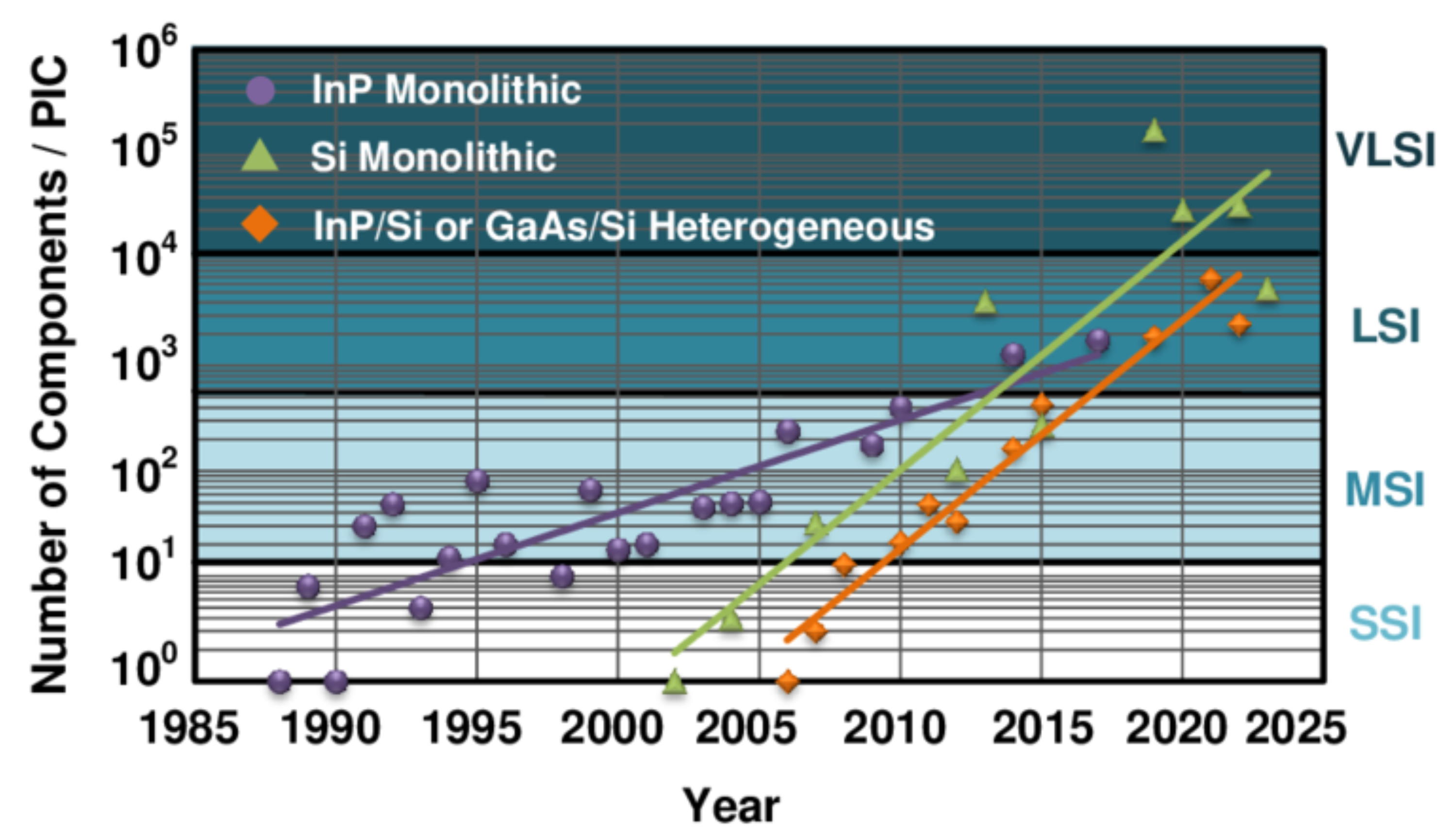
6.1. Compactness and Scalability

PICs also enhance compactness and scalability, offering key advantages for Fog and Cloud infrastructures. Traditional transceivers with discrete lasers, modulators, and photodetectors require substantial space and complicate deployment in dense environments [46]. PICs, by integrating all optical components on a single chip, dramatically reduce footprint and simplify assembly. This enables higher transmission densities and supports real-time analytics at the edge [47]. In addition, PICs support extensive wavelength division multiplexing (WDM), allowing infrastructures to scale optical bandwidth efficiently and meet growing data demands [48].

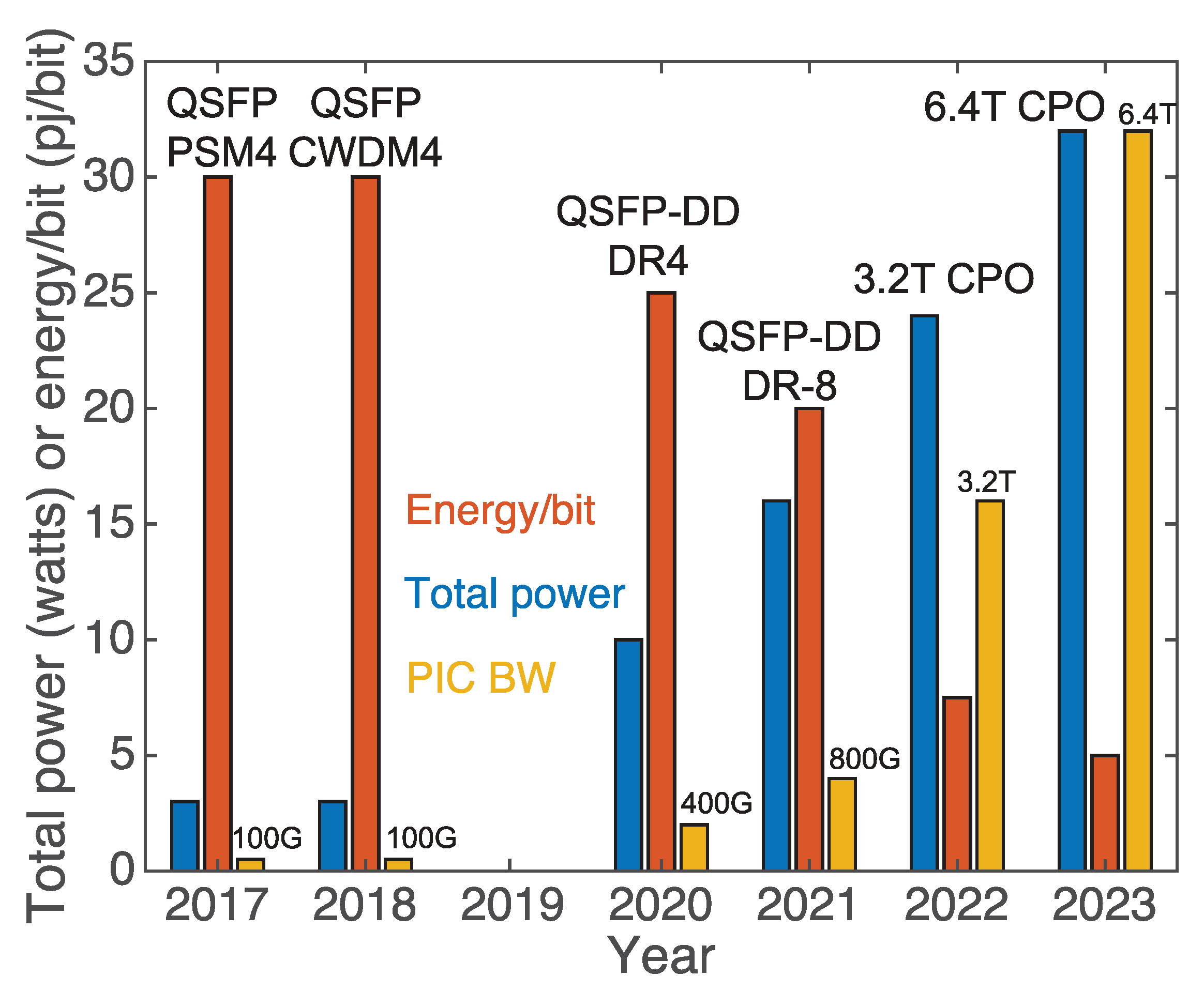
6.2. Energy Performance Trends in Photonic Integration

To address the need for a more systematic presentation of performance metrics, we include two figures summarizing the technological evolution of photonic integrated circuits (PICs). Figure 4 shows the evolution of integration densities (measured in number of components per PIC) across different platforms, including monolithic InP, monolithic silicon, and heterogeneous InP/Si or GaAs/Si systems. This timeline highlights the rapid growth in integration scale, particularly in silicon-based platforms, which have reached over 40,000 components per chip. Also, projections indicate that the integration density of heterogeneous InP/Si systems—featuring on-chip lasers and optical amplifiers—is expected to rise significantly in the near future.
Figure 5 [50], compares the energy-efficiency (in pJ/bit) of various PIC platforms over time, including both academic and commercial implementations. It provides a benchmark for evaluating power consumption trends and highlights the progress toward sub-picojoule efficiencies—an essential enabler for sustainable Fog and IoT photonic computing. PIC platforms offer a pathway to significantly more power-efficient and cost-effective systems for the future scaling of optically enabled technologies. Together, these figures illustrate the trajectory of performance improvements and help contextualize the architectures discussed in Section 4 in terms of practical scalability, energy profile, and technological maturity.
Several definitions used in Figure 5 are presented as follows: QSFP (Quad Small Form-factor Pluggable) is a compact, hot-pluggable transceiver used in data communication applications. It supports four lanes of data in each direction (quad = 4) and is typically used in 40 G and 100 G Ethernet. PSM4 (Parallel Single Mode 4-lane) is an optical link standard for 100 G Ethernet that uses four parallel single-mode fibers in each direction. Each lane operates at 25 Gbps, totaling 100 Gbps. CWDM4 (Coarse Wavelength Division Multiplexing 4-lane) is a standard for 100 G Ethernet that multiplexes four wavelengths—rather than fibers—onto a single pair of single-mode fibers, with each wavelength carrying 25 Gbps. QSFP-DD (Quad Small Form-factor Pluggable Double Density) is an evolution of the QSFP form factor. The “DD” denotes double density, offering eight electrical lanes instead of four, and supports 200 G and 400 G data rates. DR4 (100 G/400G Direct Reach 4-lane) is a standard optical interface used primarily in 400 G Ethernet. It employs four lanes of 100 G PAM4 (4-level Pulse Amplitude Modulation) signaling over parallel single-mode fiber. CPO (Co-Packaged Optics) refers to the integration of optical components (e.g., lasers, modulators) directly onto the same substrate or package as electronic switch or Application-Specific Integrated Circuit (ASIC) chips.
PIC technology significantly reduces power consumption per transmitted bit compared to traditional discrete optical transceivers by integrating key photonic elements—lasers, modulators, and detectors—onto a single chip. This consolidation minimizes losses from external connections, fiber couplings, and alignment errors [46]. Integrated architectures also reduce parasitic capacitances and shorten interconnect distances, lowering drive voltages and energy usage per bit [51]. Advanced techniques like monolithic laser integration and hybrid assembly further enhance thermal management, cutting the overhead from temperature control systems [52]. These innovations position PICs as a highly energy-efficient solution for data center interconnects, Cloud computing, and other high-performance networking environments.

6.3. Integrating CMOS Photonics with Electronic Control Circuits

Integrating CMOS photonics with electronic control circuits is pivotal for achieving compact, high-speed, and efficient optical systems. Flip-chip bonding is one prominent technique that enables direct electrical and thermal interfacing between electronic integrated circuits and photonic components fabricated using CMOS-compatible processes. This method facilitates the alignment and electrical connection of photonic and electronic chips through micro-bumps, significantly reducing parasitic capacitances and inductances, and thus enhancing bandwidth and energy-efficiency [53]. Additionally, flip-chip integration supports higher-density interconnects and improves signal integrity compared to wire-bonding methods, enabling the scalable manufacturing of photonic–electronic modules suitable for Fog computing and high-performance data center applications [54]. Alternative approaches, such as monolithic integration, 3D stacking, and through-silicon vias (TSVs), are also gaining traction due to their potential to further minimize footprint, enhance system performance, and simplify assembly processes [49].
A significant research opportunity lies in the heterogeneous integration of CMOS-compatible chips with other semiconductor platforms, such as silicon nitride (SiN), indium phosphide (InP), lithium niobate (LiNbO3), and III-V materials. While CMOS technology offers scalability, low-cost manufacturing, and mature electronics integration, it lacks the optical performance needed for certain photonic functions, such as on-chip lasing and aplification. Materials like InP support active photonic devices (e.g., lasers and amplifiers), SiN provides ultra-low-loss passive waveguides ideal for dense wavelength division multiplexing (DWDM), and LiNbO3 enables high-speed, low-power electro-optic modulation. Research is needed to develop scalable packaging, bonding, and co-fabrication techniques that allow for seamless optical and electrical interfacing between these heterogeneous platforms. Co-integration strategies could enable the development of a new class of hybrid photonic–electronic systems for Fog computing, data centers, and quantum communication, combining the best properties of each material to overcome the current limitations in monolithic PIC designs.

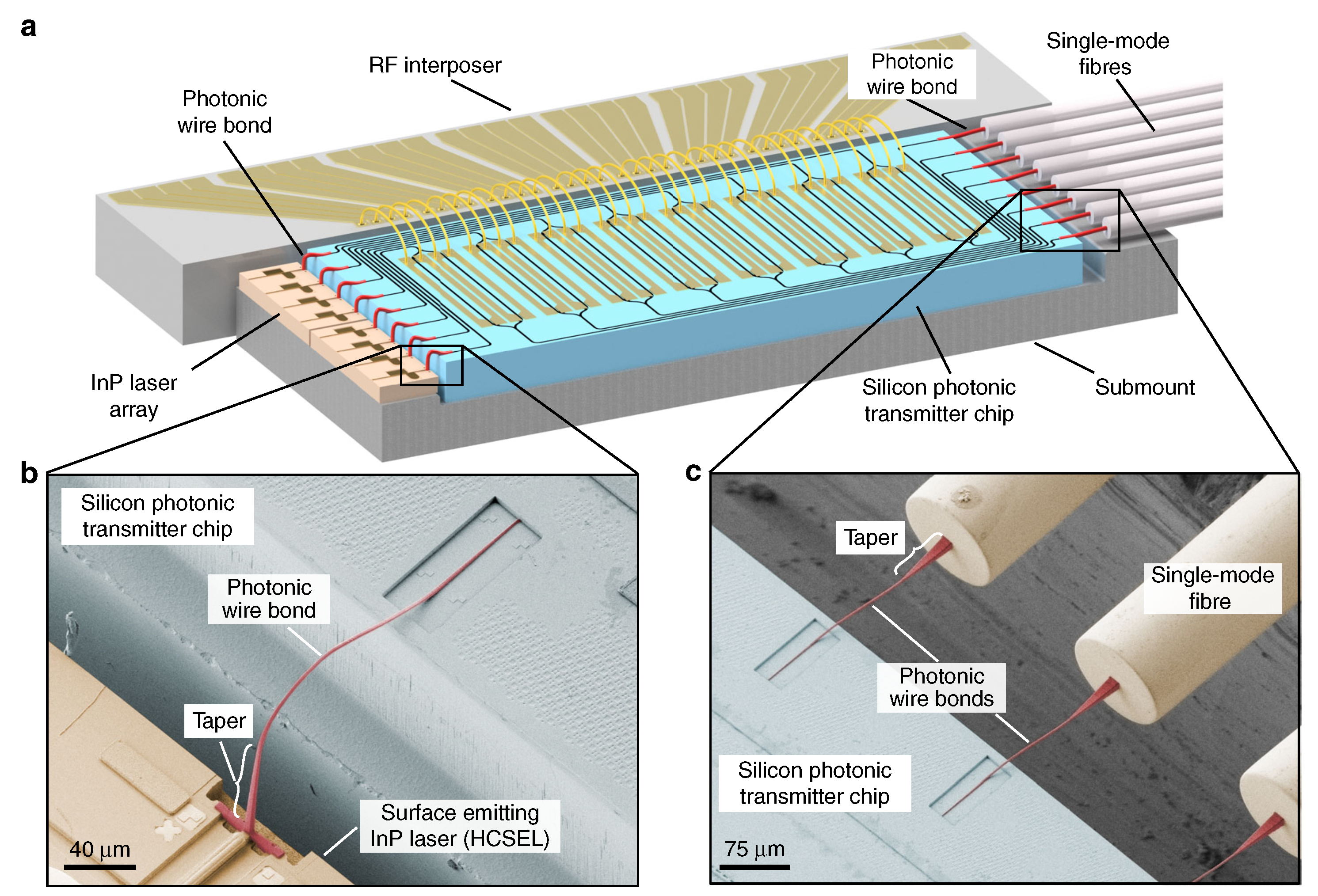
6.4. High-Speed Optical Interconnects

Recent developments in silicon photonics-based high-speed optical interconnects by industry leaders such as Intel, Cisco, IBM, and NVIDIA are significantly advancing Fog and Cloud computing by addressing bandwidth, latency, and energy-efficiency challenges. Intel’s Optical Compute Interconnect (OCI) chiplet enables direct ultra-high-bandwidth data transfer within computing modules, which is essential for Fog environments requiring fast edge processing [3]. Cisco’s 1.6 Tbps OSFP-XD transceivers support efficient, high-speed interconnects in dense Cloud data centers, reducing power usage while boosting scalability for rapidly growing AI and data workloads [55]. IBM’s co-packaged optics (CPO) with polymer waveguides and NVIDIA’s Quantum-X800 InfiniBand switch, which leverages silicon photonics, both enhance throughput and reduce latency for AI-driven, hybrid Cloud–Fog platforms [56,57]. Together, these technologies highlight the foundational role of optical interconnects in shaping next-generation distributed computing systems.
Figure 6 illustrates the full assembly of a co-packaged optical switch system, highlighting sixteen transceiver modules closely co-packaged with a central switch application-specific integrated circuit (ASIC). This compact arrangement significantly enhances bandwidth density, reduces electrical link lengths, and minimizes power consumption, which are essential for addressing escalating demands in data center environments. By directly integrating optical transceivers and electronics into a unified assembly, this CPO architecture mitigates traditional interconnection bottlenecks and enables a scalable, energy-efficient interconnect solution suitable for future high-capacity switch deployments [58].
The rising demands of Fog and Cloud infrastructures necessitate fast, low-latency, and energy-efficient data links—needs well met by PIC technologies. Broadcom’s 51.2 Tbps CPO switch, with eight integrated optical engines, boosts bandwidth density while reducing energy use [59]. Marvell’s 1.6 Tbps silicon photonics engine, demonstrated at OFC 2025, integrates drivers and amplifiers for compact, low-power interconnects in AI networks [60]. Infinera’s multi-functional PICs, MACOM’s L-PIC platform, and Lightmatter’s Passage M1000 superchip further reduce power and cost while supporting high-speed workloads [61,62,63]. Additionally, Ranovus’ Odin platform and DustPhotonics’ Tamar200 module offer monolithic, multi-terabit PIC solutions for next-generation hyperscale deployments [64,65]. Collectively, these innovations emphasize the strategic importance of photonic interconnects in scaling Cloud and Fog computing architectures.

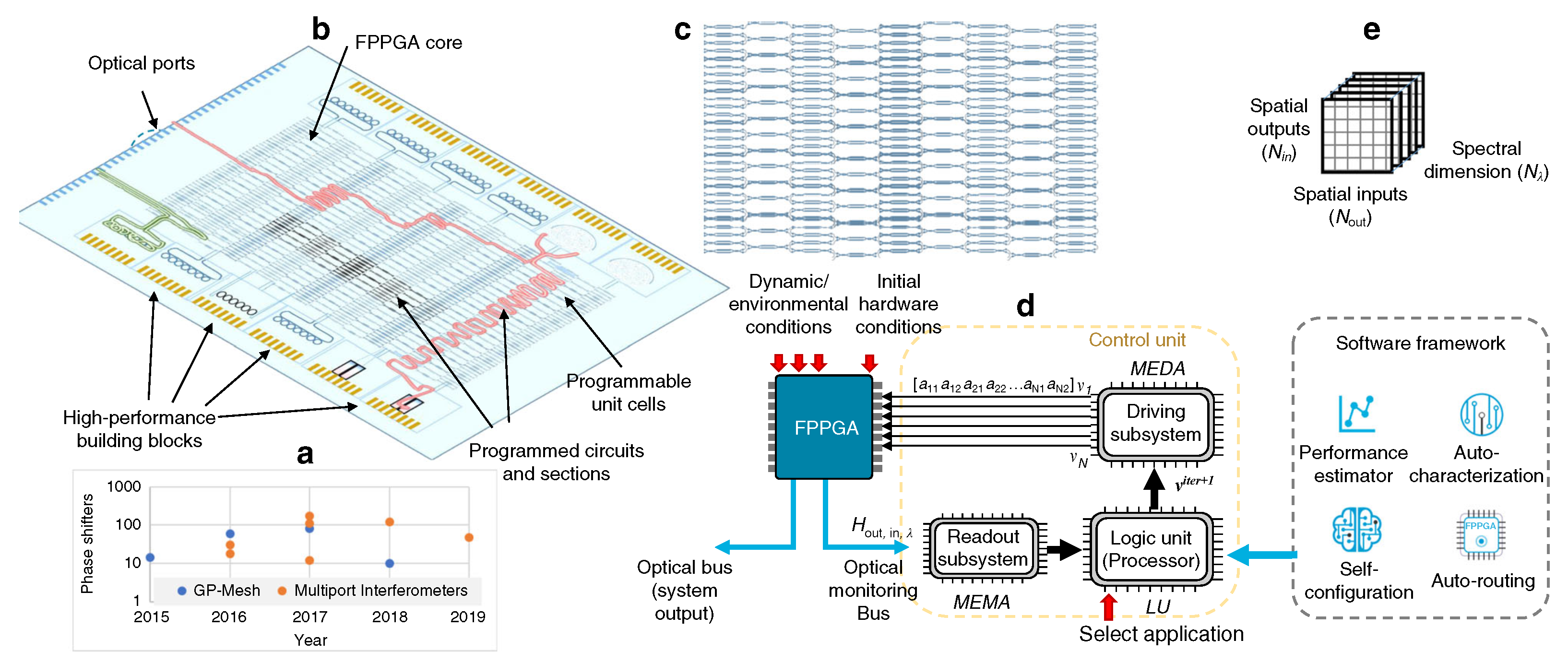
6.5. Optical Switching and Routing

PIC technology presents a transformative approach to data routing, signal processing, and traffic management in both Fog and Cloud computing environments. Unlike traditional optical communication systems, which rely heavily on intermediate optical-to-electrical (O/E) and electrical-to-optical (E/O) conversions for routing and processing, PIC-based architectures enable the direct manipulation of optical signals on-chip. In conventional systems, incoming optical data must be photodetected and converted into the electrical domain for processing and retransmission, a sequence that introduces significant latency, increases energy consumption, and constrains scalability in high-speed and distributed computing scenarios [66].
PICs overcome these limitations by integrating essential optical components—such as switches, multiplexers, modulators, and wavelength-selective routers—into a compact, chip-scale platform. This integration enables all-optical routing and switching at the speed of light, eliminating the need for electronic conversions and allowing for faster, more energy-efficient data transport [67]. These capabilities are especially critical for Fog computing, where real-time responsiveness is essential to support mission-critical applications such as autonomous vehicles, smart grids, and industrial automation. In hyperscale Cloud data centers, the ability to handle vast amounts of data with lower latency and energy per operation is equally vital for improving user experience and maintaining high service levels under peak demand [68].
Beyond latency reduction, PICs offer substantial improvements in system scalability and energy-efficiency. By minimizing the number of active electronic components and interconnects, PIC-enabled architectures reduce thermal loads and simplify cooling infrastructure, contributing to lower operational costs. Furthermore, the integration of photonic interconnects allows for shorter data paths and higher aggregate throughput, directly benefiting computer-intensive tasks like AI inference, big data analytics, and real-time video processing [69,70].
Another significant advantage of PICs is their capacity to support dynamic and adaptive traffic management. Traditional optical networks often rely on static, manually configured paths and electronic control planes, which struggle to respond to fluctuating workloads in distributed computing environments. PICs enable reconfigurability through the integration of tunable filters, variable optical attenuators, and high-speed optical switches, allowing for network resources to be allocated in real-time based on current bandwidth demands, latency requirements, or fault conditions [71]. This level of agility is indispensable for emerging edge-centric applications and for enhancing the Quality of Service (QoS) in Cloud infrastructures. By introducing programmability and reconfigurability at the photonic level, PICs lay the foundation for scalable, future-proof network architectures [72].

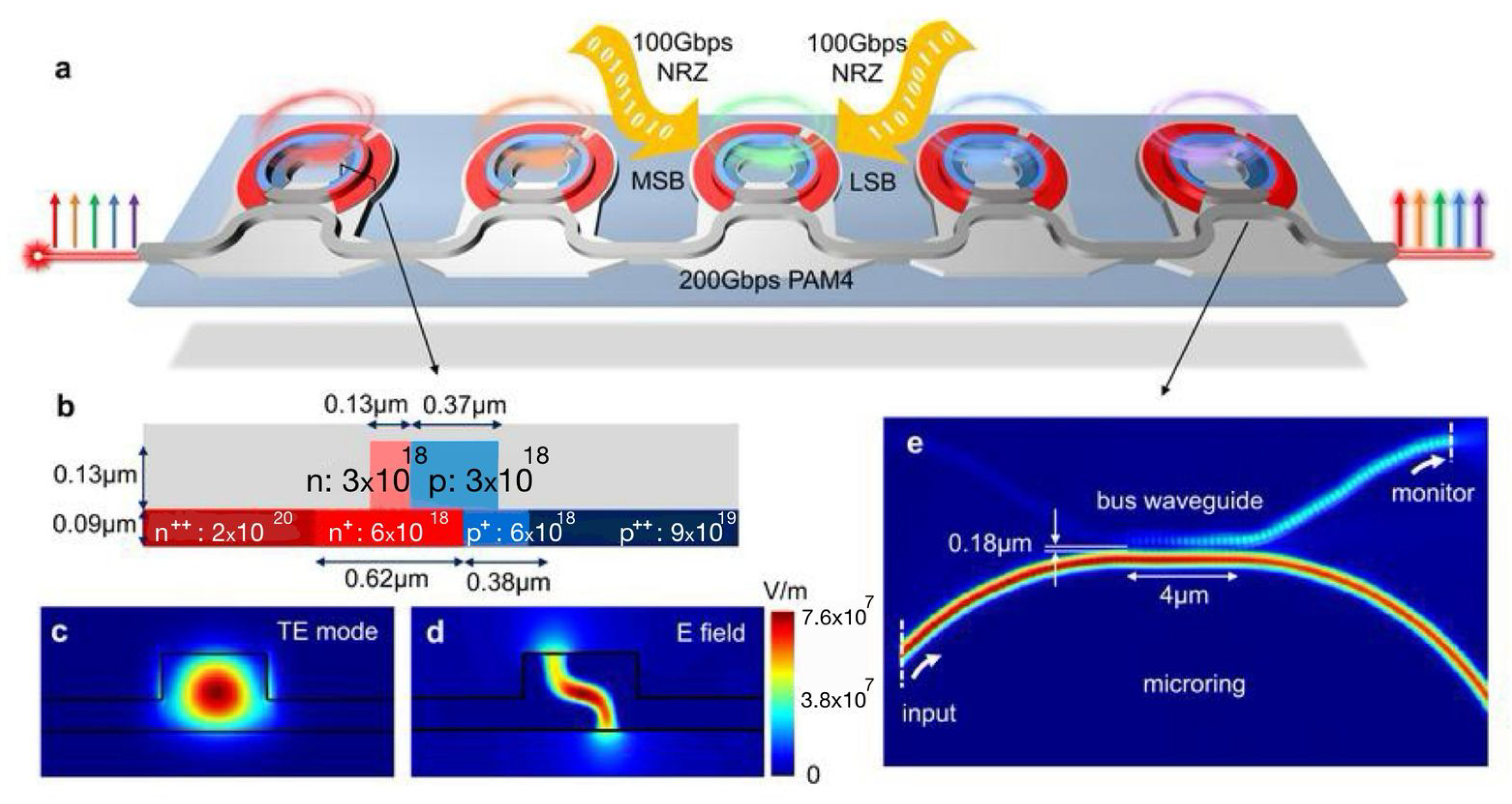
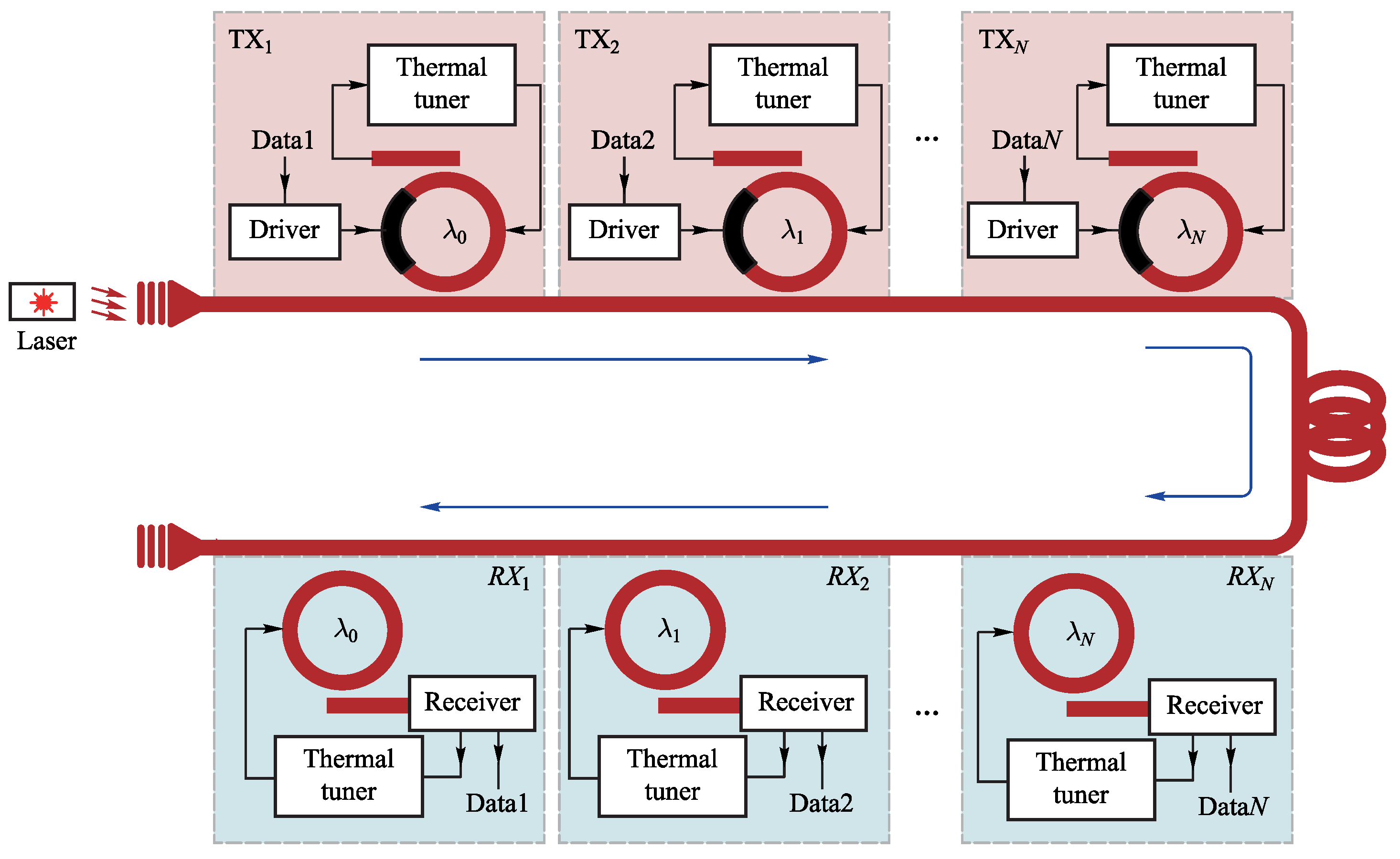
6.6. Wavelength Division Multiplexing (WDM)

PICs with WDM functionalities are essential building blocks for enabling high-throughput and energy-efficient optical communication in Fog and Cloud computing environments. Unlike discrete optical systems, WDM PICs integrate components such as modulators, multiplexers, and photodetectors on a single chip, reducing footprint, latency, and power consumption. This subsection highlights several key implementations of WDM transmitters and receivers using silicon photonics. These examples demonstrate how PIC-based WDM architectures are well-suited to the bandwidth, latency, and integration demands of next-generation Fog and Cloud networks. Traditional WDM systems based on discrete components struggle with scalability and integration density. Recent advances have produced ultra-compact, broadband, multi-dimensional multiplexed PICs that significantly increase data throughput while minimizing footprint [73]. These innovations support the real-time processing and high-speed transmission of large data volumes. Their integration also reduces system complexity and power consumption, supporting the energy-efficiency goals of modern data centers [74]. As Fog computing brings processing closer to the edge and Cloud systems scale globally, PIC-based multiplexing becomes essential for seamless, high-capacity optical communication.
Figure 7 illustrates two key demonstrations of silicon photonic WDM-integrated circuits. In part (A), a 40-channel WDM receiver PIC is shown, which integrates a silicon nitride arrayed waveguide grating (AWG) with germanium photodetectors. The device achieves flattened passbands and supports single-channel operation at data rates up to 40 Gb/s, as shown in the eye diagram inset. In part (B), a compact 10 × 25 Gb/s DWDM transmitter is presented, which integrates single-drive push–pull Mach–-Zehnder modulators and a silicon nitride AWG on a 5 × 8 mm2 chip. Each channel exhibits a clear eye-opening at 25 Gb/s after wavelength multiplexing, demonstrating the viability of dense WDM transmission using silicon PICs [75].
Another key device that can be used for long-haul, Fog and Cloud optical networks is the Mach–Zehender modulator (MZM). Figure 8 depicts a schematic view of a single-drive MZM designed in silicon-on-insulator (SOI) technology with a 250 nm active silicon layer. This modulator uses transversal electric (TE) mode grating couplers to couple light between single-mode optical fibers and the integrated waveguides, followed by linear tapers for mode adaptation. Multimode interference (MMI) couplers symmetrically split and recombine optical signals across two interferometric branches. The modulation functionality is realized through carrier-depletion effects in one branch, induced by the doping and reverse biasing of silicon waveguides connected via metal vias to an RF coplanar transmission line. The other branch includes a delay line to ensure appropriate phase shifts for effective modulation. This configuration provides a compact, CMOS-compatible platform, enabling efficient optical modulation suitable for high-speed optical communication systems [76].
One device that can act as a filter and as a modulator is the microring. Figure 9 illustrates the detailed structure and operational principles of the two-segment Z-shape junction silicon micro-ring modulators (MRMs) [77]. Panel (a) presents the layout of the five-channel dense-wavelength division multiplexing (DWDM) array, highlighting variations in the ring radius to facilitate evenly spaced resonance wavelengths. Panel (b) details the Z-shape doping profile, showing its specific arrangement within the silicon waveguide, which is strategically designed to optimize the overlap between carrier depletion regions and the optical mode. Panels (c) and (d) display simulations of the transverse electric (TE) mode and electric field distribution within the waveguide, respectively, demonstrating effective modulation under reverse-bias conditions. Finally, panel (e) provides a finite-difference time-domain (FDTD) simulation depicting the coupling region of the microring modulator to a bus waveguide for monitoring.
Figure 10 presents a schematic illustration of a micro-ring resonator (MRR)-based transceiver array employed in co-packaged optics (CPO). The depicted transceiver integrates drivers, micro-ring modulators (MRMs), and receivers with an MRR-based demultiplexer (DEMUX) and thermal tuning mechanisms. This architecture addresses key performance constraints such as bandwidth, energy-efficiency, and compactness, that are essential for future data center optical interconnects. Hybrid and monolithic integration methods have demonstrated data rates of up to 112 Gb/s per channel, achieving high energy-efficiency despite the challenges posed by parasitic capacitances and integration complexities. Thermal tuning is critical to stabilize resonant wavelengths against variations induced by manufacturing processes and operating conditions [58].

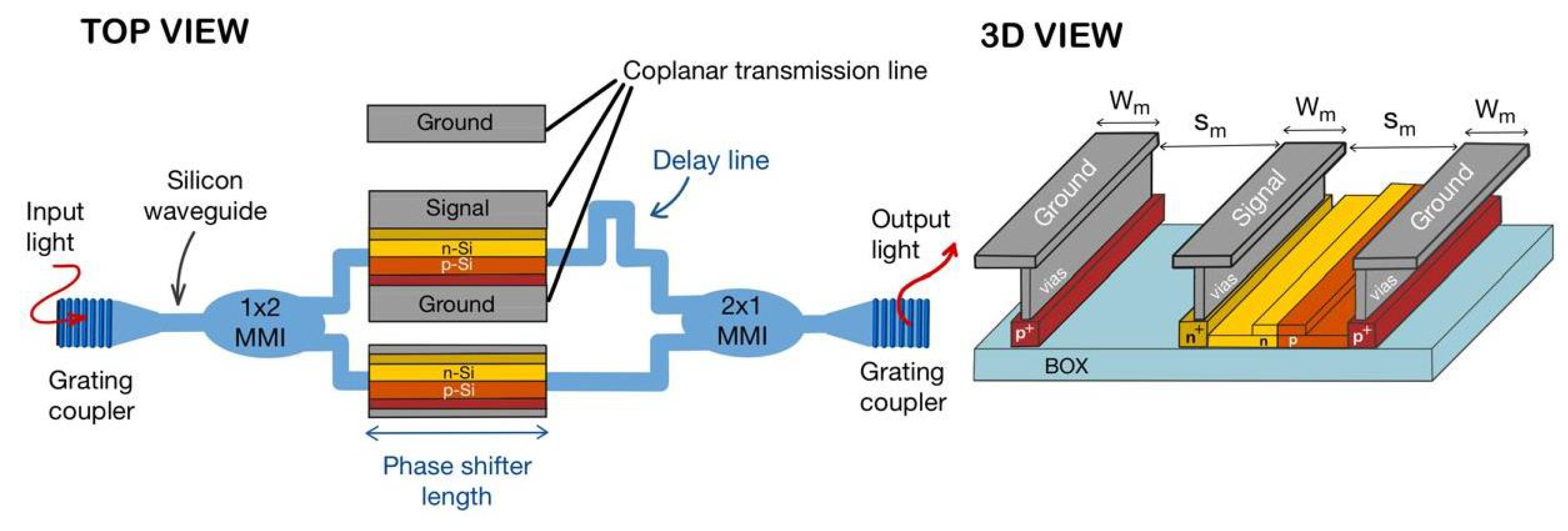
6.7. Coherent Optics

PIC technology plays a critical role in enabling ultra-high spectral efficiency, long-distance transmission, and scalable optical capacity for next-generation Fog and Cloud computing infrastructures. By integrating advanced modulation formats such as QAM and coherent on-chip detection, PICs allow for compact, low-loss, and high-bit-rate transmission systems that maximize spectral usage [78]. These functions are difficult to achieve with discrete components due to alignment challenges and signal degradation. Additionally, PICs support ultra-dense wavelength division multiplexing (UDWDM) and polarization multiplexing within a single platform, enhancing throughput without increasing fiber infrastructure [79]. Their ability to reduce insertion losses and incorporate on-chip amplification extends transmission reach and lowers the need for regeneration, which is essential for high-capacity Cloud backbones and low-latency Fog deployments.
Moreover, PICs are ideally suited for the high-speed interconnection of geographically distributed data centers—a growing requirement for edge analytics, content delivery, and global-scale computing. Unlike traditional interconnects based on discrete optical elements, PIC-based transceivers integrate coherent optics, modulators, multiplexers, and FEC, supporting long-haul links over hundreds to thousands of kilometers with low power consumption and minimal signal degradation [80,81]. These integrated transceivers also support software-defined networking (SDN), enabling dynamic bandwidth allocation and real-time traffic management across optical backbones [74]. Together, these features make PICs foundational to building energy-efficient, scalable, and globally interconnected Fog and Cloud computing systems.
Figure 11 presents a four-channel PIC coherent transmitter module demonstrating advanced hybrid integration techniques at both the chip and package levels [82]. Panel (a) provides an overview of the multi-chip module comprising InP-based HCSEL laser sources, silicon–organic hybrid (SOH) IQ modulators, and single-mode fibers interconnected by photonic wire bonds (PWBs). Panel (b) details the structure of the SOH Mach-Zehnder modulators, emphasizing the precise deposition of electro-optic material within silicon slot waveguides for efficient modulation. Panel (c) outlines the experimental setup used for coherent transmission experiments, involving modulation via an arbitrary-waveform generator, propagation through 75 km of fibre, and subsequent coherent detection. Finally, panel (d) shows representative constellation diagrams along with measured bit error ratios at high symbol rates, underscoring the feasibility of achieving reliable high-speed communication with this hybrid integration approach.

6.8. Quantum and Advanced Computing

PIC technology plays a foundational role in emerging paradigms such as quantum computing, quantum communication, and neuromorphic computing—each poised to reshape Fog and Cloud architectures. PICs are well-suited to quantum photonic systems due to their low-loss, phase-stable, and scalable optical paths, enabling the integration of sources, beam-splitters, phase shifters, and detectors on a single chip for quantum logic and entanglement distribution [83]. In quantum communication, PICs support secure, high-speed links between Fog nodes and Cloud cores via quantum key distribution (QKD), enhancing data security across distributed systems [84]. Neuromorphic computing, which mimics brain-like parallel processing, also benefits from photonic implementations that enable ultra-fast, energy-efficient edge AI and sensory fusion in Fog environments [67]. These innovations empower distributed infrastructures to handle complex tasks—such as encryption, inference, and real-time learning—locally, while reserving heavier computation for the Cloud. As a result, PICs provide the hardware foundation for scalable, cognitive, and secure Fog–Cloud ecosystems.
Companies like PsiQuantum and Intel are advancing integrated photonic chips for quantum computing, with major implications for distributed architectures. PsiQuantum leverages photonic circuits and existing semiconductor manufacturing to develop scalable, fault-tolerant quantum computers aimed at deployment in global data centers [85]. Intel is developing silicon-based spin-qubit processors with integrated photonic components for high-fidelity qubit control and readout, supporting compact quantum modules suitable for Fog and Cloud environments [86]. Collectively, these efforts highlight how integrated photonics can enable seamless, high-performance quantum computing across distributed computing networks.
Table 4 provides an overview of key PIC technologies relevant to Fog and Cloud computing. It highlights the current state of the art and outlines emerging research opportunities across integration, interconnects, energy-efficiency, and advanced computing paradigms.

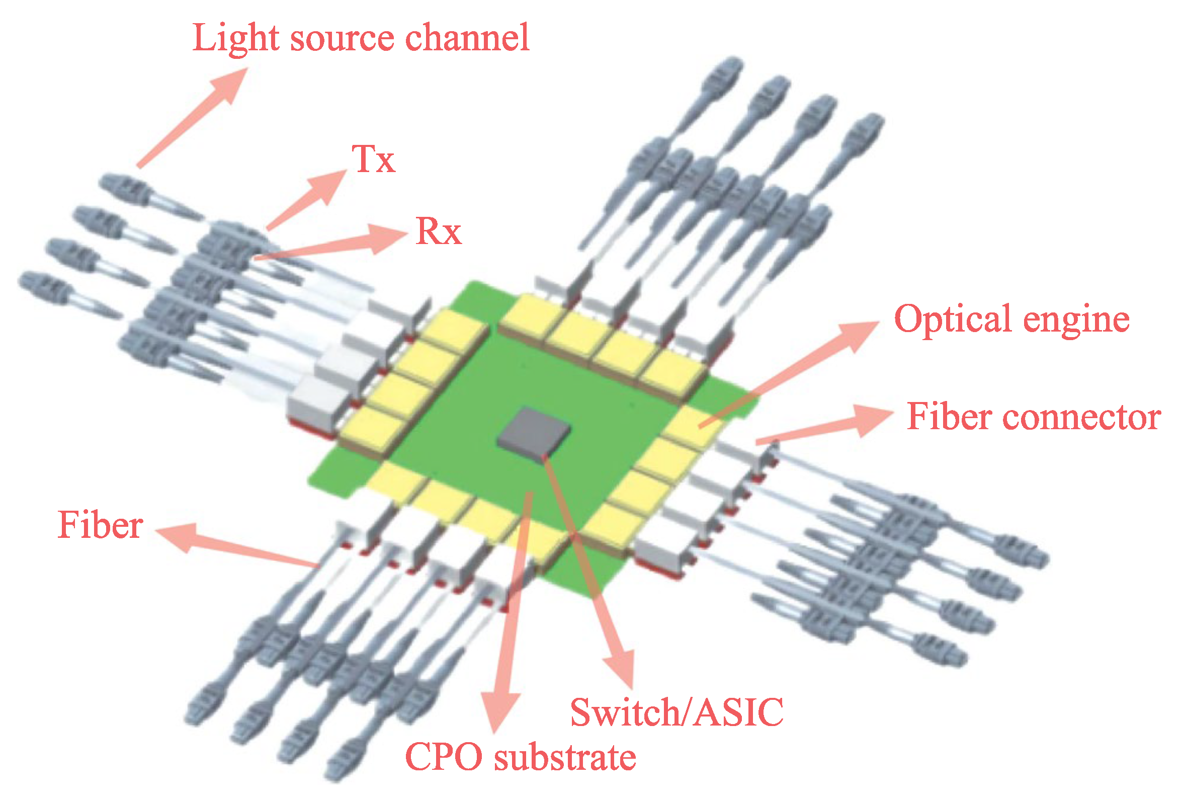
7. Industry Implementations

Major technology companies are increasingly adopting PIC technology to meet the performance, scalability, and energy-efficiency demands of Fog and Cloud computing infrastructures. Intel and Cisco have emerged as industry leaders in deploying silicon photonic transceivers. Intel’s optical I/O chiplet integrates lasers, modulators, and photodetectors on a single silicon photonics platform, enabling up to 4 Tbps of low-latency, high-bandwidth communication between CPUs, accelerators, and memory nodes—which is essential for hyperscale Cloud environments [3]. Cisco, in partnership with Accelink, has introduced 1.6 Tbps OSFP-XD silicon photonic transceivers based on dense wavelength division multiplexing (DWDM), which significantly increase fiber capacity while maintaining compact, energy-efficient form factors [55]. These solutions are particularly valuable for AI-driven data center operations and latency-sensitive Fog computing scenarios. Intel is also pursuing co-packaged optics (CPO) to eliminate traditional electrical I/O bottlenecks, integrating PICs directly into switch ASICs to reduce energy per bit and improve signal integrity compared to short-reach high-density connections. Cisco’s roadmap includes the expanded adoption of coherent PICs within metro and long-haul transport platforms, leveraging integrated DSPs and tunable lasers to increase link adaptability and spectral utilization [87].
Nokia and Fujitsu are also contributing to the commercialization of PIC technologies. Nokia’s latest optical transport innovations include 800G coherent pluggable optics and multi-haul WDM systems integrated into advanced line systems [88], as well as deployment with partners like CoreWeave to support an AI-optimized Cloud infrastructure [89]. These platforms are designed to deliver high-capacity, energy-efficient, and latency-aware connectivity across hyperscale data centers and distributed Fog nodes. In parallel, research by Meng et al. has demonstrated the use of integrated photonic digital-to-analog converters (DACs) for on-chip high-speed optical signal generation, addressing electronic bottlenecks and improving throughput, latency, and spectral efficiency in wide-area Fog–Cloud networks [90]. Nokia is further investing in programmable photonics for software-defined optical networks and has presented silicon photonic switches capable of rapid reconfiguration [91]. Fujitsu, on the other hand, is focusing on integrated RoF platforms using PICs to simplify front-haul deployment in dense urban environments, a key asset for edge-based 5G/6G architectures [92].
Programmable photonic circuits can be viewed as optical analogues of electronic Field-Programmable Gate Arrays (FPGAs), enabling dynamic reconfiguration and multifunctionality for photonic applications [93]. Unlike traditional fixed photonic integrated circuits, these systems can adapt their functionality post-fabrication, enabling multiple operations such as signal routing, modulation, and filtering on a single chip. This programmability drastically reduces development time, lowers manufacturing costs, and enhances scalability, making them especially advantageous in applications requiring flexible analog processing such as telecommunications, data centers, quantum information systems, and artificial intelligence. Furthermore, programmable photonic circuits incorporate self-configuration capabilities, mitigating the effects of fabrication imperfections and environmental variations through intelligent control algorithms [93]. Figure 12 illustrates the integrated photonic hardware and associated electronic control architecture used in multipurpose programmable photonic circuits. Panel (a) highlights the growing complexity of state-of-the-art photonic integration, characterized by the increasing number of integrated phase shifters. Panel (b) depicts the general architecture of a field-programmable photonic gate array (FPPGA), featuring a programmable waveguide mesh core surrounded by specialized high-performance building blocks and optical input/output ports. Panel (c) provides a detailed view of the FPPGA core, implemented with a longitudinally parallel hexagonal waveguide mesh interconnection topology. The electronic control subsystem, shown in panel (d), includes essential elements such as a driving subsystem for configuring the waveguide mesh, an optical monitoring subsystem for feedback, and software algorithms for auto-routing and self-configuration. Lastly, panel (e) conceptually represents the comprehensive scattering matrix that characterizes the input–output relationships across both spatial and spectral domains within the FPPGA core, enabling detailed system-level programming and optimization.
Meta (formerly Facebook) and Microsoft are advancing integrated photonics to overcome the limitations of traditional pluggable optical modules in data center interconnects (DCIs). Meta promotes the co-packaging of optics with switch electronics to reduce power consumption by 20% and improve scalability via automated manufacturing processes compatible with CMOS technology [94]. Complementing this, energy-proportional data center architectures co-designed at the system and photonic levels allow for optical paths to be activated dynamically based on traffic needs—achieving up to 60% energy savings in optical transceivers while sustaining performance [95]. These strategies align well with the dynamic and variable workloads inherent in Fog computing. Microsoft has also collaborated with optical foundries to develop silicon photonics-based multi-wavelength transceivers and is exploring neuromorphic photonic processors for future acceleration workloads in edge-cloud environments [96]. Additionally, both companies contribute to open-source hardware initiatives for photonic–electronic co-packaged modules to promote industry-wide standardization and supply chain diversity [97].
Amazon Web Services (AWS) is also actively investing in integrated photonics. In collaboration with STMicroelectronics, AWS developed a photonics chip designed to boost internal bandwidth and reduce power consumption in AI data centers [98]. By replacing conventional electrical data transmission with light-based interconnects in transceivers, AWS targets lower latency and energy use at massive scale. The chip is expected to enter deployment later this year, with production based in STMicroelectronics’ Crolles, France facility. This marks a significant milestone in moving toward more sustainable and high-performance distributed computing infrastructure. AWS is also funding research into hybrid InP/Si photonic integration to extend performance into longer reach links [99], and evaluating photonic tensor cores for low-latency inference tasks within their serverless compute platforms [67]. These initiatives reflect a broader strategy to maintain infrastructure leadership amid rapidly growing AI/ML workloads.
The global photonic ecosystem is rapidly evolving thanks to a vibrant startup landscape and strategic initiatives by regional governments. Startups such as Ayar Labs, Lightmatter, Rockley Photonics, and Optalysys are leveraging programmable photonics, optical interconnects, and neuromorphic architectures to create domain-specific accelerators and compact sensor platforms [91,100,101]. These firms bridge the gap between research and industrial deployment by using open-access design platforms and collaborative prototyping models. Supporting this transition, open-foundry initiatives like IMEC’s Europractice, AIM Photonics in the US, JePPIX in Europe, and Ligentec for SiN-based platforms provide cost-effective access to fabrication through multi-project wafer (MPW) runs [91,102]. Additionally, public–private consortia such as the European Union’s PIXAPP and PhotonHub Europe [103] and U.S. government programs under DARPA’s LUMOS and iFAB [104] are accelerating the commercialization pipeline by standardizing packaging, offering design kits, and expanding photonic design education. Together, these efforts are democratizing PIC development and supporting its broader adoption in Fog, Cloud, and edge computing infrastructures.
Despite rapid progress, the widespread industrial deployment of photonic integrated circuits still faces key bottlenecks across multiple dimensions. Thermal sensitivity remains a major challenge, especially for silicon and III-V platforms, where temperature fluctuations induce refractive index changes that degrade performance and stability [105]. Packaging and fiber–chip coupling also represent significant hurdles: grating couplers, edge couplers, and photonic wire bonding introduce insertion losses that affect system-level efficiency [106]. Manufacturing variability, particularly lithographic and etching errors during wafer fabrication, leads to component mismatch and yield loss, although recent advances in inverse design and digital calibration offer partial remedies [107]. Testing is another bottleneck, as high-throughput wafer-level characterization tools for photonics are still underdeveloped compared to electronic ICs [108]. These challenges highlight the need for co-optimization across materials, fabrication, packaging, and electronic–photonic co-design to unlock the full potential of PICs in large-scale distributed systems.
Figure 13 illustrates the concept and implementation of hybrid multi-chip modules (MCMs) enabled by 3D nano-printing of photonic wire bonds (PWBs) [82]. Panel (a) shows a conceptual eight-channel transmitter module where PWBs, depicted in red, efficiently interconnect photonic integrated circuits (PICs) fabricated on different material platforms, such as InP lasers and silicon photonic modulators. Panels (b) and (c) provide detailed views of the laser-to-chip and fibre-to-chip interfaces, respectively, highlighting how PWBs adapt their geometry to match mode-field profiles for low-loss coupling, thereby eliminating the need for high-precision active alignment.
National strategies in both the United States and Europe are accelerating the integration of photonic and electronic technologies to strengthen digital infrastructure and semiconductor independence. In the U.S., the CHIPS and Science Act and DARPA’s LUMOS program support the development of CMOS-compatible PICs through funding, foundry access, and laser integration research [104,109]. Meanwhile, Europe is advancing through Horizon Europe and PhotonHub initiatives, promoting open-access innovation, photonic–electronic co-design, and high-yield manufacturing via coordinated industry–academic consortia such as EPIC [103]. These efforts highlight a global push toward the development of scalable, power-efficient PIC ecosystems for data-intensive and latency-sensitive applications.
To address these industrial bottlenecks, leading companies and research consortia are implementing a variety of strategies. For thermal sensitivity, thermal stabilization techniques such as micro-ring trimming, athermal design using cladding engineering, and feedback-controlled heaters have been deployed in commercial silicon photonics platforms [105]. For packaging and coupling challenges, advanced approaches like photonic wire bonding, self-aligning connectorized packaging, and 3D-printed optical interfaces are being developed to reduce insertion loss and improve alignment tolerance [110]. To combat manufacturing variability, foundries now increasingly use inverse design frameworks—the automated shape optimization of photonic devices with tolerance analysis—and apply digital tuning during the runtime using on-chip heaters or phase shifters [111]. On the testing side, AI-driven wafer inspection tools and integrated test photonics (e.g., built-in monitors and loopbacks) are enabling scalable, real-time diagnostics [112]. Co-design strategies that align photonic and electronic components from the system architecture level are also gaining traction to simultaneously improve yield and performance. These efforts indicate a clear industrial pivot toward holistic PIC design workflows that integrate photonic layout, thermal control, testing hooks, and packaging early in the development cycle, accelerating the path toward reliable, high-volume deployment in distributed computing networks.
Table 5 summarizes the main advantages of integrated photonics in Fog–Cloud computing.

8. Future Trends

A key trend in PIC technology is the rise of co-packaged optics (CPO), which integrates optical transceivers directly onto processor or switch packages. This eliminates the need for traditional pluggable modules, greatly reducing electrical interconnect length, latency, power consumption, and physical footprint while boosting bandwidth density [74]. In Cloud computing, CPO supports ultra-scalable, high-throughput networks ideal for AI, ML, and real-time analytics. For Fog computing, CPO enables compact, low-latency systems by tightly coupling compute and communication functions [3]. Companies such as Intel, Broadcom, and NVIDIA are advancing CPO platforms to overcome performance and efficiency bottlenecks in distributed infrastructures. As such, CPO is a key enabler of the bandwidth- and energy-efficient architectures needed across Cloud cores and Fog nodes.
PICs are also emerging as powerful hardware accelerators for machine learning, offering advantages in speed, energy-efficiency, and parallelism. Unlike electronic processors, PICs perform matrix-vector multiplications—the core of neural networks—using light, enabling ultrafast, low-power computation [67]. Optical neural networks (ONNs) implemented on silicon photonic chips can execute inference and training tasks with far less energy than GPUs, making them ideal for real-time, low-power AI at the edge. In Cloud environments, PICs support scalable AI acceleration for large deep learning models, enhancing throughput and reducing cost per operation [117]. As AI workloads continue to grow, PIC-based processors offer a transformative leap in performance for both centralized and edge computing.
PICs are also foundational to optical computing and neuromorphic photonics, which use light rather than electrons for computation. In optical computing, PICs bypass electronic bottlenecks—such as RC delays and heat dissipation—to enable ultrafast, energy-efficient operations that are ideal for matrix operations and real-time analytics [68]. Neuromorphic photonics leverages nonlinear optics, phase modulation, and feedback to emulate brain-like spiking neural networks [67]. At the edge, this enables fast, low-power sensory and AI processing for autonomous systems and smart infrastructure. In the Cloud, these processors support scalable training and analytics for massive datasets. Together, these advances position PIC-based optical computing as a cornerstone of future distributed Fog–Cloud systems.
Another transformative trend in photonic integration is the development of programmable photonic circuits (PPCs), which provide reconfigurable light pathways using tunable elements such as thermo-optic or electro-optic phase-shifters. PPCs support applications ranging from quantum computing to AI inference and offer adaptability akin to field-programmable gate arrays (FPGAs) in electronics [91]. These architectures enable the dynamic reconfiguration of signal routing, filtering, and logic at the photonic level, which is crucial for versatile, scalable Fog and Cloud platforms. Beyond academic labs, programmable photonics are being adopted by startups like Lightelligence and Lightmatter, and are finding utility in heterogeneous data-processing environments that require low-latency signal-steering and AI pipeline acceleration. Their inclusion in next-generation optical processors opens the door to flexible, software-defined photonic computing systems.
In parallel, advances in photonic quantum information-processing and neuromorphic design paradigms are positioning PICs at the frontier of next-generation computing. Leveraging the quantum properties of photons—such as superposition and entanglement—quantum photonic chips allow for ultra-secure communication and massively parallel computing schemes [118,119]. These advances could enable photonic architectures that go beyond von Neumann models, targeting problems in optimization, cryptography, and real-time pattern recognition. When deployed in hybrid Fog–Cloud systems, photonic quantum processors and neuromorphic modules could support edge intelligence with unprecedented speed, energy-efficiency, and data security. These capabilities are particularly relevant to autonomous systems, environmental sensing, and real-time AI-enabled services, suggesting a profound role for PICs in shaping future distributed computing landscapes.
Integrating optical neural networks into real-time, edge-deployable systems remains an open area, with several efforts focusing on simulating optical neural networks for deep learning workloads in edge computing environments [120]. Advances in photonic packaging and co-design with electronics are critical—as demonstrated by NTT’s Photonics–Electronics Convergence (PEC) roadmap, which places integrated transmitters and receivers progressively closer to CPU/ASIC chips, moving toward the use of die-to-die optical interconnects by 2032 [121]. Furthermore, hybrid architectures combining classical, neuromorphic, and quantum photonics require unified design frameworks: recent research into hybrid quantum–classical photonic neural networks outlines pathways to enhance computational capacity without expanding network size [122]. Addressing these gaps is essential for transitioning from isolated PIC modules to holistic, intelligent photonic computing platforms that bridge the edge-to-cloud continuum.

9. Summary of Benefits

Integrated photonics offers a transformative set of advantages for both Fog and Cloud networks, enabling next-generation distributed computing architectures. In Fog computing, PICs provide ultra-low-latency, compact form factors, and energy-efficient data-processing—ideal for real-time applications at the network edge, such as in autonomous vehicles, industrial IoT, and smart infrastructure. In Cloud data centers, integrated photonics supports ultra-high bandwidth, scalable interconnects, and CPO, reducing power consumption and enabling denser compute fabrics for AI and data-intensive workloads. Across both layers, PICs facilitate dynamic traffic management, increased spectral efficiency, and extended transmission distances through wavelength division multiplexing (WDM) and coherent optics. Furthermore, their compatibility with optical computing, neuromorphic photonics, and quantum technologies positions integrated photonics as a foundational technology for secure, high-performance, and future-proof Fog–Cloud ecosystems.

10. Implementation Challenges and Emerging Solutions

The adoption of photonic integrated circuits (PICs) in distributed computing environments such as Cloud, Fog, and IoT infrastructures brings numerous implementation challenges that go beyond mere component integration. These include systemic, manufacturing, and deployment-specific barriers. In what follows, we discuss the most significant challenges and emerging solutions, integrating recent insights from the silicon photonics roadmap literature [49].
One critical challenge lies at the system level, where thermal sensitivity and thermal crosstalk threaten the performance and stability of dense PICs. Due to the compact integration of active and passive optical elements, even minor thermal fluctuations can cause phase drift, wavelength shifts, and performance degradation in modulators and resonators. Recent works emphasize that thermal crosstalk—where heat generated by one element affects neighboring components—is becoming a limiting factor in high-density layouts [49,123]. Emerging solutions include the use of thermal-aware placement and routing algorithms, thermally isolating materials, and the development of athermal resonator designs. Additionally, self-adjusting circuits with real-time feedback control are being investigated to ensure operational stability is maintained under variable thermal conditions.
Another challenge is the lack of scalable and cost-effective packaging and optical coupling techniques. Traditional methods such as fiber arrays or active alignment remain expensive and difficult to automate. As the number of input/output ports in PICs increases, so does the difficulty of ensuring low-loss and high-reliability connections. To address this, approaches such as photonic wire bonding, polymer waveguides, and grating couplers have been introduced. These techniques offer more tolerance of alignment errors and are compatible with automated assembly [49]. Photonic wire bonding provides a flexible, high-throughput solution for connecting chips of different technologies or geometries.
Manufacturability represents a third major barrier. Variability in fabrication processes leads to nonuniform performance across dies and wafers. This is especially problematic in resonance-based devices, where nanometer-scale deviations can cause substantial wavelength shifts. Strategies such as inverse design, digital calibration, and self-configuration are gaining traction as solutions. Inverse design leverages optimization algorithms to create structures that are less sensitive to fabrication errors. Meanwhile, digital calibration techniques—some assisted by machine learning—allow circuits to auto-tune after packaging to compensate for imperfections [49,124].
An increasingly important challenge, highlighted by Bogaerts et al. [49], is the complexity of PIC design and the lack of standardized design methodologies. Unlike digital electronics, where designers rely on reusable IP blocks and mature CAD tools, photonic design still lacks widespread abstraction layers and standard cell libraries. This increases the design burden and lengthens development cycles. Initiatives to develop more comprehensive photonic design kits (PDKs), along with machine learning-based design automation tools, are showing promise. Such tools aim to democratize photonic design and reduce entry barriers for system-level engineers.
Testing and debugging PICs is another under-addressed issue. While electronics can be tested at the wafer scale using electrical probes, optical I/O requires specialized and often manual alignment setups. Built-in self-test (BIST) strategies, on-chip monitors, and reconfigurable test structures are proposed as solutions to improve scalability and reduce test costs. Automated wafer-scale optical testing is also a focus of current R&D, particularly for high-volume applications [49].
A structural challenge that hinders PIC innovation—especially in academia and startups—is limited access to foundry services. Unlike electronics, where multi-project wafer (MPW) services are standardized and frequent, silicon photonics faces long fabrication delays, infrequent access, and limited support for novel designs. Most MPW programs prioritize high-volume industrial clients, restricting research prototyping and increasing both cost and risk. Initiatives like AIM Photonics (USA), JePPIX (EU), and EUROPRACTICE aim to broaden access via standardized PDKs and subsidized MPW runs. However, PDK limitations and pipeline rigidity persist. Greater foundry support and open-access, modular design flows are needed to make the photonic ecosystem as agile and scalable as its electronic counterpart, especially for Cloud, Fog, and IoT applications [49].
Finally, deployment-specific constraints—especially in Fog and Edge environ- ments—impose tight requirements on size, energy, and environmental resilience. While Cloud data centers can accommodate large-scale cooling systems and redundant designs, Fog nodes must be compact, power-efficient, and ruggedized for varied operating conditions [10]. This necessitates modular packaging solutions, thermally adaptive components, and PIC architectures that can gracefully degrade or self-reconfigure under stress. These features are critical to enable robust operation in mobile, outdoor, or constrained environments.
In summary, while PICs hold immense promise for high-speed, low-energy, and scalable communication and computation, their widespread deployment depends on overcoming multi-layered challenges. The integration of design automation, manufacturing innovation, thermal control strategies, and self-tuning mechanisms will be crucial in transitioning PICs from research labs to large-scale deployment in Cloud and Fog infrastructures.

11. Conclusions

PIC technology represents a foundational advancement for the evolution of Fog and Cloud computing infrastructures. By enabling ultra-fast, energy-efficient, and compact optical communication and processing capabilities, PICs address the core challenges of scalability, latency, and bandwidth in distributed systems. In Cloud data centers, PICs power high-throughput optical interconnects, co-packaged optics, and advanced AI acceleration platforms, all while dramatically reducing power consumption and improving spectral efficiency. At the Fog layer, where compact, low-power, and real-time responsiveness are essential, PICs support optical computing, neuromorphic photonics, and edge AI workloads with unmatched latency performance and integration density. Industry leaders such as Intel, Cisco, Microsoft, Meta, Amazon, Nokia, and Fujitsu are already implementing PIC-based solutions, highlighting the critical role of photonics in next-generation networks. Whether through quantum communication, dynamic traffic routing, or long-haul data center interconnects, PICs serve as the physical layer enablers of secure, intelligent, and responsive computing ecosystems. As the demands of decentralized and AI-driven infrastructures increase, integrated photonics will be essential for building future-proof, high-performance Fog and Cloud architectures.

Author Contributions

Formal analysis, G.A.C.Á., W.C. and A.M.S.-M.; Writing—review & editing, G.A.C.Á., W.C. and A.M.S.-M. All authors have read and agreed to the published version of the manuscript.

Funding

This research was funded by Secretaría de Ciencia, Humanidades, Tecnología e Innovación (SeCiHTI).

Data Availability Statement

The raw data supporting the conclusions of this article will be made available by the authors on request.

Conflicts of Interest

The authors declare no conflicts of interest.

References

  1. Morichetti, F. High-performance analog signal processing with photonic integrated circuits. Light Sci. Appl. 2025, 14, 141. [Google Scholar] [CrossRef] [PubMed]
  2. Li, R.; Gong, Y.; Huang, H.; Zhou, Y.; Mao, S.; Wei, Z.; Zhang, Z. Photonics for Neuromorphic Computing: Fundamentals, Devices, and Opportunities. Wiley Adv. Mater. 2024, 37, 2312825. [Google Scholar] [CrossRef] [PubMed]
  3. Intel Corporation. Intel Demonstrates First Fully Integrated Optical I/O Chiplet. 2025. Available online: https://newsroom.intel.com/artificial-intelligence/intel-unveils-first-integrated-optical-io-chiplet (accessed on 4 May 2025).
  4. Nvidia Corporation. Nvidia Is Planning Post-Copper 1.6 Tbps Network Tech to Connect Millions of GPUs as It Unveils Photonics Networking Gear at GTC 2025. Available online: https://www.techradar.com/pro/nvidia-is-planning-post-copper-1-6tbps-network-tech-to-connect-millions-of-gpus-as-it-unveils-photonics-networking-gear-at-gtc-2025 (accessed on 11 April 2025).
  5. Zhang, Y.; Li, R.; Wang, H.; Liu, Y.; Chen, X. Integrated Photonic Processor Implementing Digital Image Convolution. Electronics 2025, 14, 709. [Google Scholar] [CrossRef]
  6. Chiang, M.; Zhang, T. Fog and IoT: An overview of research opportunities. IEEE Internet Things J. 2016, 3, 854–864. [Google Scholar] [CrossRef]
  7. Baliga, J.; Ayre, R.W.A.; Hinton, K.; Tucker, R.S. Green Cloud Computing: Balancing Energy in Processing, Storage, and Transport. Proc. IEEE 2011, 99, 149–167. [Google Scholar] [CrossRef]
  8. Radamson, H.H.; Miao, Y.; Zhou, Z.; Wu, Z.; Kong, Z.; Gao, J.; Yang, H.; Ren, Y.; Zhang, Y.; Shi, J.; et al. CMOS Scaling for the 5 nm Node and Beyond: Device, Process and Technology. Nanomaterials 2024, 14, 837. [Google Scholar] [CrossRef]
  9. Capmany, J.; Novak, D. Microwave photonics combines two worlds. Nat. Photonics 2007, 1, 319–330. [Google Scholar] [CrossRef]
  10. Marpaung, D.; Yao, J.; Capmany, J. Integrated microwave photonics. Nat. Photonics 2019, 13, 80–90. [Google Scholar] [CrossRef]
  11. Qian, T.; Schuler, B.; Gupta, Y.D.; Deumer, M.; Andrianopoulos, E.; Lyras, N.K.; Kresse, M.; Weigel, M.; Reck, J.; Mihov, K.; et al. Hybrid Photonic Integrated Circuits for Wireless Transceivers. Photonics 2025, 12, 371. [Google Scholar] [CrossRef]
  12. Beas, J.; Castanon, G.; Aldaya, I.; Aragón-Zavala, A.; Campuzano, G. Millimeter-Wave Frequency Radio over Fiber Systems: A Survey. IEEE Commun. Surv. Tutor. 2013, 15, 1593–1619. [Google Scholar] [CrossRef]
  13. Aldaya, I.; Beas, J.; Castanon, G.; Campuzano, G.; Aragón-Zavala, A. A Survey of Key-Enabling Components for Remote Millimetric Wave Generation in Radio over Fiber Networks. Opt. Laser Technol. 2013, 49, 213–226. [Google Scholar] [CrossRef]
  14. EMCORE Corporation. PIC Technology :: EMCORE Corporation. 2025. Available online: https://www.emcore.com/support/pic-technology (accessed on 11 April 2025).
  15. AIM Photonics. What Is Integrated Photonics. 2025. Available online: https://www.aimphotonics.com/what-is-integrated-photonics (accessed on 11 April 2025).
  16. Castanon, G.; Campuzano, G.; Tonguz, O.K. High reliability and availability in radio over fiber networks. J. Opt. Netw. 2008, 7, 603–617. [Google Scholar] [CrossRef]
  17. Moon, S.R.; Sung, M.; Kim, E.; Lee, J.K.; Cho, S.H.; Kim, J. Hybrid radio-over-fiber transport system to support heterogeneous indoor mobile network environments. J. Opt. Commun. Netw. 2024, 16, 71–80. [Google Scholar] [CrossRef]
  18. Kase, Y.; Hori, S.; Oshima, N.; Kunihiro, K. Radio-over-Fiber Systems with 1-bit Outphasing Modulation for 5G/6G Indoor Wireless Communication. NEC Tech. J. 2023, 17, 1–6. [Google Scholar] [CrossRef]
  19. Abdalla, A.M.; Rodriguez, J.; Elfergani, I.; Teixeira, A. Optical and Wireless Convergence for 5G Access Networks, 1st ed.; Wiley-IEEE Press: Piscataway, NJ, USA, 2019. [Google Scholar]
  20. Pech, M.; Vrchota, J.; Bednář, J. Predictive Maintenance and Intelligent Sensors in Smart Factory: Review. Sensors 2021, 21, 1470. [Google Scholar] [CrossRef]
  21. Mouradian, C.; Naboulsi, D.; Yangui, S.; Glitho, R.H.; Morrow, M.J.; Polakos, P.A. A Comprehensive Survey on Fog Computing: State-of-the-Art and Research Challenges. IEEE Commun. Surv. Tutor. 2018, 20, 416–464. [Google Scholar] [CrossRef]
  22. Xu, J.; Dong, W.; Huang, Q.; Zhang, Y.; Yin, Y.; Zhao, Z.; Zeng, D.; Gao, X.; Gu, W.; Yang, Z.; et al. Progress in silicon-based reconfigurable and programmable all-optical signal processing chips. Front. Optoelectron. 2025, 18, 10. [Google Scholar] [CrossRef]
  23. Lin, Y.; Yong, Z.; Luo, X.; Azadeh, S.S.; Mikkelsen, J.C.; Sharma, A.; Chen, H.; Mak, J.C.C.; Lo, P.G.Q.; Sacher, W.D.; et al. Monolithically integrated, broadband, high-efficiency silicon nitride-on-silicon waveguide photodetectors in a visible-light integrated photonics platform. Nat. Commun. 2022, 13, 6636. [Google Scholar] [CrossRef]
  24. Cao, R.; He, Y.; Zhu, Q.; Li, J.; An, S.; Zhang, Y.; Su, Y. Multi-channel 28-GHz millimeter-wave signal generation on a silicon photonic chip with automated polarization control. J. Semicond. 2019, 40, 1–7. [Google Scholar] [CrossRef]
  25. Wang, Y.; Lin, Y.; Chen, L.; Shi, J. A Stackelberg Game-Based Caching Incentive Scheme for Roadside Units in VANETs. Sensors 2020, 20, 6625. [Google Scholar] [CrossRef]
  26. Anderson, P.; Aranas, E.B.; Assaf, Y.; Behrendt, R.; Black, R.; Caballero, M.; Cameron, P.; Canakci, B.; De Carvalho, T.; Chatzieleftheriou, A. Project Silica: Towards Sustainable Cloud Archival Storage in Glass. In Proceedings of the SOSP 23: Proceedings of the 29th Symposium on Operating Systems Principles, Koblenz, Germany, 23–26 October 2023; Volume 29, pp. 166–181. [Google Scholar] [CrossRef]
  27. Ahmad, A.; Jan, M.U.; Shah, S.A.; Kaleem, Z.; Ahmad, B.; Ahmed, I.; Alam, M.M.; Khan, I. Edge Intelligence in Private Mobile Networks for Next-Generation Railway Systems. Front. Commun. Netw. 2021, 2, 769299. [Google Scholar] [CrossRef]
  28. Butt, M.A.; Mateos, X.; Piramidowicz, R. Photonics sensors: A perspective on current advancements, emerging challenges, and potential solutions (Invited). Phys. Lett. A 2024, 516, 129633. [Google Scholar] [CrossRef]
  29. Antonacci, G.; Goyvaerts, J.; Zhao, H.; Baumgartner, B.; Lendl, B.; Baets, R. Ultra-sensitive refractive index gas sensor with functionalized silicon nitride photonic circuits. APL Photonics 2020, 5, 081301. [Google Scholar] [CrossRef]
  30. PhotonFirst. Fiber Optic Sensing Solutions. 2025. Available online: https://www.photonfirst.com/ (accessed on 21 April 2025).
  31. Hänsel, A.; Adamu, A.I.; Markos, C.; Feilberg, A.; Bang, O.; Heck, M.J.R. Integrated Ammonia Sensor Using a Telecom Photonic Integrated Circuit and a Hollow Core Fiber. Photonics 2020, 7, 93. [Google Scholar] [CrossRef]
  32. Surfix Diagnostics. Photonic Diagnostics Platform for Point-of-Care Testing. 2025. Available online: https://www.surfixdx.com/ (accessed on 21 April 2025).
  33. PHOSFOS Consortium. PHOSFOS—Photonic Skins for Optical Sensing. Available online: https://en.wikipedia.org/wiki/PHOSFOS (accessed on 21 April 2025).
  34. Shamy, R.S.E.; Swillam, M.A.; Li, X. Optimization of Silicon Nitride Waveguide Platform for On-Chip Virus Detection. Sensors 2022, 22, 1152. [Google Scholar] [CrossRef]
  35. Shamy, R.S.E.; Swillam, M.A.; Li, X. Comparative Study of Photonic Platforms and Devices for On-Chip Sensing. Photonics 2023, 10, 1233. [Google Scholar] [CrossRef]
  36. Nava, M.; Castanon, G. Numerical analysis of a SiN digital Fourier transform spectrometer for a non-invasive glucose monitor. Appl. Opt. 2025, 64, 1–5. [Google Scholar] [CrossRef]
  37. Reuters. EU-Backed Consortium to Develop Efficient Sensors for Satellite Navigation. 2024. Available online: https://www.reuters.com/technology/space/eu-backed-consortium-develop-efficient-sensors-satellite-navigation-2024-07-03/ (accessed on 21 April 2025).
  38. Han, K.; Long, D.A.; Bresler, S.M.; Song, J.; Bao, Y.; Reschovsky, B.J.; Srinivasan, K.; Gorman, J.J.; Aksyuk, V.A.; LeBrun, T.W. Low-power, agile electro-optic frequency comb spectrometer for integrated sensors. Optica 2024, 11, 392–398. [Google Scholar] [CrossRef]
  39. Narukage, N.; Ishikawa, Y.; Sakao, T.; Wang, X. High-speed back-illuminated CMOS sensor for photon-counting-type imaging-spectroscopy in the soft X-ray range. Nucl. Instrum. Methods Phys. Res. Sect. A Accel. Spectrometers Detect. Assoc. Equip. 2019, 940, 162974. [Google Scholar] [CrossRef]
  40. Ponizovskaya-Devine, E.; Mayet, A.S.; Rawat, A.; Ahamed, A.; Wang, S.Y.; Elrefaie, A.F.; Yamada, T.; Islam, M.S. Single microhole per pixel for thin Ge-on-Si complementary metal-oxide semiconductor image sensor with enhanced sensitivity up to 1700 nm. J. Nanophotonics 2023, 17, 016012. [Google Scholar] [CrossRef]
  41. Hakkel, K.D.; Petruzzella, M.; Ou, F.; van Klinken, A.; Pagliano, F. Integrated near-infrared spectral sensing. Nat. Commun. 2022, 13, 1–9. [Google Scholar] [CrossRef] [PubMed]
  42. Van Gerven, P. Amazec Recycles ASML Technology to Diagnose Heart Failure. Available online: https://bits-chips.nl/artikel/amazec-recycles-asml-technology-to-diagnose-heart-failure/ (accessed on 21 April 2025).
  43. Zhao, Y.; Zhao, M.; Fu, J.; Yang, X.; Yang, S.; Xu, Y.; Wang, X.; Zhang, S.; Song, T.; Liu, Y.; et al. Nanostructured Temperature Indicator for Cold Chain Logistics. ACS Nano 2022, 16, 8641–8650. [Google Scholar] [CrossRef]
  44. Hong, M.; Sima, C.; Sun, Y.; Xu, J.; Li, K.; Zhang, L.; Wang, L.; Ming, Z.; Lu, P. Monolithically integrated passive photonic silicon chip for nano-g level acceleration tri-axial detection. Opt. Express 2025, 33, 5945–5957. [Google Scholar] [CrossRef]
  45. Zhang, L.; Zhang, X.; Wei, W.; Dai, Y.; Feng, X.; Zhu, W.; Wang, Y.; Zhang, Z.; Guan, X.; He, J. Detection of Volatile Organic Compounds Using Mid-Infrared Silicon Nitride Waveguides. Sci. Rep. 2022, 12, 9597. [Google Scholar] [CrossRef]
  46. Thomson, D.; Zilkie, A.; Bowers, J.E.; Komljenovic, T.; Reed, G.T. Roadmap on silicon photonics. J. Opt. 2016, 18, 073003. [Google Scholar] [CrossRef]
  47. Shi, Y.; Zhang, Y.; Wan, Y.; Yu, Y.; Zhang, Y.; Hu, X.; Xiao, X.; Xu, H.; Zhang, L.; Pan, B. Silicon photonics for high-capacity data communications. Photonics Res. 2022, 10, A106–A134. [Google Scholar] [CrossRef]
  48. Smit, M.K.; Williams, K.; van der Tol, J. Past, present, and future of InP-based photonic integration. APL Photonics 2019, 4, 050901. [Google Scholar] [CrossRef]
  49. Shekhar, S.; Bogaerts, W.; Chrostowski, L.; Bowers, J.E.; Hochberg, M.; Soref, R.; Shastri, B.J. Roadmapping the next generation of silicon photonics. Nat. Commun. 2024, 15, 751. [Google Scholar] [CrossRef]
  50. Margalit, N.; Xiang, C.; Bowers, S.M.; Bjorlin, A.; Blum, R.; Bowers, J.E. Perspective on the future of silicon photonics and electronics. Appl. Phys. Lett. 2021, 118, 220501. [Google Scholar] [CrossRef]
  51. Reed, G.T.; Knights, A.P. Silicon Photonics: An Introduction, 2nd ed.; Wiley: Hoboken, NJ, USA, 2022. [Google Scholar] [CrossRef]
  52. Rahim, A.; Hermans, A.; Wohlfeil, B.; Petousi, D.; Kuyken, B.; Thourhout, D.V.; Baets, R. Taking silicon photonics modulators to a higher performance level: State-of-the-art and a review of new technologies. Adv. Photonics 2021, 3, 024003. [Google Scholar] [CrossRef]
  53. Hochberg, M.; Baehr-Jones, T. Silicon Photonics: The Next Fabless Semiconductor Industry. IEEE Solid-State Circuits Mag. 2013, 5, 48–58. [Google Scholar] [CrossRef]
  54. Doany, F.E.; Schow, C.L.; Lee, B.G.; Budd, R.A.; Kash, J.A. Terabit/s-Class Optical PCB Links Incorporating 360-Gb/s Bidirectional 850 nm Parallel Optical Transceivers. J. Light. Technol. 2012, 30, 560–571. [Google Scholar] [CrossRef]
  55. Cisco Systems and Accelink Technologies. Accelink and Cisco Collaborate on 1.6 T OSFP-XD Silicon Photonics Transceiver. 2024. Available online: https://www.accelink.com/en/lighting_your_dreams/1772863410472550402.html (accessed on 16 April 2025).
  56. IBM Corporation. IBM Brings the Speed of Light to the Generative AI Era with Optics Breakthrough. 2024. Available online: https://newsroom.ibm.com/2024-12-09-ibm-brings-the-speed-of-light-to-the-generative-ai-era-with-optics-breakthrough (accessed on 16 April 2025).
  57. NVIDIA Corporation. NVIDIA Announces Spectrum-X Photonics, Co-Packaged Optics Networking Switches for AI Factories. 2025. Available online: https://nvidianews.nvidia.com/news/nvidia-spectrum-x-co-packaged-optics-networking-switches-ai-factories (accessed on 16 April 2025).
  58. Tan, M.; Xu, J.; Liu, S.; Feng, J.; Zhang, H.; Yao, C.; Chen, S.; Guo, H.; Han, G.; Wen, Z.; et al. Co-packaged optics (CPO): Status, challenges, and solutions. Front. Optoelectron. 2023, 16, 1. [Google Scholar] [CrossRef] [PubMed]
  59. Broadcom Inc. Broadcom Delivers Industry’s First 51.2-Tbps Co-Packaged Optics Switch. 2024. Available online: https://investors.broadcom.com/news-releases/news-release-details/broadcom-delivers-industrys-first-512-tbps-co-packaged-optics (accessed on 16 April 2025).
  60. Marvell Technology Group Ltd. Marvell Demonstrates Silicon Photonics Light Engine for Low-Power, Rack-Scale Interconnect in AI Networks. 2025. Available online: https://www.marvell.com/company/newsroom/marvell-demonstrates-silicon-photonics-light-engine-for-low-power-rack-scale-interconnect-in-ai-networks.html (accessed on 16 April 2025).
  61. Infinera Corporation. Photonic Integrated Circuits Pioneered by Infinera. 2025. Available online: https://www.infinera.com/innovation/photonic-integrated-circuit/ (accessed on 16 April 2025).
  62. MACOM Technology Solutions. MACOM Enabling Rapid Transition to 400G for Cloud Data Centers with L-PIC Platform. 2017. Available online: https://ir.macom.com/news-releases/news-release-details/macom-enabling-rapid-transition-400g-cloud-data-centers-l-pictm (accessed on 16 April 2025).
  63. Lightmatter. Lightmatter Unveils Passage M1000 Photonic Superchip, World’s Fastest AI Interconnect. 2025. Available online: https://lightmatter.co/press-release/lightmatter-unveils-passage-m1000-photonic-superchip-worlds-fastest-ai-interconnect/ (accessed on 16 April 2025).
  64. RANOVUS Inc. ODIN® Single-chip Optical Engine. 2025. Available online: https://ranovus.com/odin/ (accessed on 16 April 2025).
  65. DustPhotonics. DustPhotonics Expands Silicon Photonics Portfolio with 2xFR4 Products for AI and Hyperscale Data Centers. 2025. Available online: https://www.dustphotonics.com/dustphotonics-expands-silicon-photonics-portfolio-with-2xfr4-products-for-ai-and-hyperscale-data-centers/ (accessed on 17 April 2025).
  66. Miller, D.A.B. Optical interconnects to electronic chips. Appl. Opt. 2010, 49, F59–F70. [Google Scholar] [CrossRef]
  67. Shastri, B.J.; Tait, A.N.; Ferreira de Lima, T.B.; Pernice, W.H.P.; Bhaskaran, H.; Wright, C.D.; Prucnal, P.R. Photonics for artificial intelligence and neuromorphic computing. Nat. Photonics 2021, 15, 102–114. [Google Scholar] [CrossRef]
  68. Tait, A.N.; Nahmias, M.A.; Tian, Y.; Shastri, B.J.; Prucnal, P.R. Photonic Neuromorphic Signal Processing and Computing. In Nanophotonic Information Physics: Nanointelligence and Nanophotonic Computing; Naruse, M., Ed.; Springer: Berlin/Heidelberg, Germany, 2014; pp. 183–222. [Google Scholar] [CrossRef]
  69. Mekawey, H.; Elsayed, M.; Ismail, Y.; Swillam, M.A. Optical Interconnects Finally Seeing the Light in Silicon Photonics: Past the Hype. Nanomaterials 2022, 12, 485. [Google Scholar] [CrossRef]
  70. Bahadori, M.; Rumley, S.; Nikolova, D.; Bergman, K. Comprehensive Design Space Exploration of Silicon Photonic Interconnects. J. Light. Technol. 2016, 34, 2975–2987. [Google Scholar] [CrossRef]
  71. Rumley, S.; Bahadori, M.; Polster, R.; Hammond, S.D.; Calhoun, D.M.; Wen, K.; Rodrigues, A.; Bergman, K. Optical interconnects for extreme scale computing systems. Parallel Comput. 2017, 64, 65–80. [Google Scholar] [CrossRef]
  72. Shacham, A.; Bergman, K.; Carloni, L.P. Photonic networks-on-chip for future generations of chip multiprocessors. IEEE Trans. Comput. 2008, 57, 1246–1260. [Google Scholar] [CrossRef]
  73. Zhou, W.; Zhang, Z.; Chen, H.; Tsang, H.K.; Tong, Y. Ultra-compact and efficient integrated multichannel mode multiplexer in silicon for few-mode fibers. Laser Photonics Rev. 2024, 18, 2300460. [Google Scholar] [CrossRef]
  74. IEEE. 2023 IRDS Outside System Connectivity–Co-Packaged Optics and Beyond. 2023. Available online: https://irds.ieee.org/images/files/pdf/2023/2023IRDS_OSC.pdf (accessed on 16 April 2025).
  75. Dong, P.; Chen, Y.K.; Duan, G.H.; Neilson, D.T. Silicon photonic devices and integrated circuits. Nanophotonics 2014, 3, 215–228. [Google Scholar] [CrossRef]
  76. Félix Rosa, M.; Rathgeber, L.; Elster, R.; Hoppe, N.; Föhn, T.; Schmidt, M.; Vogel, W.; Berroth, M. Design of a carrier-depletion Mach-Zehnder modulator in 250 nm silicon-on-insulator technology. Adv. Radio Sci. 2017, 15, 269–281. [Google Scholar] [CrossRef]
  77. Yuan, Y.; Peng, Y.; Sorin, W.V.; Cheung, S.; Huang, Z.; Liang, D.; Fiorentino, M.; Beausoleil, R.G. A 5 × 200 Gbps microring modulator silicon chip empowered by two-segment Z-shape junctions. Nat. Commun. 2024, 15, 918. [Google Scholar] [CrossRef] [PubMed]
  78. Geng, Y.; Huang, X.; Cui, W.; Ling, Y.; Xu, B.; Zhang, J.; Yi, X.; Wu, B.; Huang, S.W.; Qiu, K.; et al. Terabit optical OFDM superchannel transmission via coherent carriers of a hybrid chip-scale soliton frequency comb. Opt. Lett. 2018, 43, 2406–2409. [Google Scholar] [CrossRef]
  79. Guan, X.; Shi, W.; Rusch, L.A. Ultra-Dense Wavelength-Division Multiplexing With Microring Modulator. J. Light. Technol. 2021, 39, 4300–4306. [Google Scholar] [CrossRef]
  80. Slook, M.; Bag, S.K.; Katzman, M.; Munk, D.; Kaganovskii, Y.; Rosenbluh, M.; Inbar, N.; Shafir, I.; Dokhanian, L.; Priel, M.; et al. 16-channel O-band silicon-photonic wavelength division multiplexer with a 1 nm channel spacing. Opt. Continuum. 2022, 1, 2135–2145. [Google Scholar] [CrossRef]
  81. Seiler, P.M.; Georgieva, G.; Winzer, G.; Peczek, A.; Voigt, K.; Lischke, S.; Fatemi, A.; Zimmermann, L. Toward coherent O-band data center interconnects. Front. Optoelectron. 2021, 14, 414–425. [Google Scholar] [CrossRef]
  82. Blaicher, M.; Billah, M.R.; Kemal, J.; Hoose, T.; Marin-Palomo, P.; Hofmann, A.; Kutuvantavida, Y.; Kieninger, C.; Dietrich, P.I.; Lauermann, M.; et al. Hybrid multi-chip assembly of optical communication engines by in situ 3D nano-lithography. Light Sci. Appl. 2020, 9, 71. [Google Scholar] [CrossRef]
  83. Wang, J.; Sciarrino, F.; Laing, A.; Thompson, M.G. Integrated photonic quantum technologies. Nat. Photonics 2020, 14, 273–284. [Google Scholar] [CrossRef]
  84. Sibson, P.; Kennard, J.E.; Peters, N.A.; Miki, S.; Yamashita, T.; Fujiwara, M.; Sasaki, M.; Terai, H.; Tanner, M.G.; Natarajan, C.M.; et al. Chip-based quantum key distribution. Nat. Commun. 2017, 8, 13984. [Google Scholar] [CrossRef]
  85. PsiQuantum. Building the World’s First Useful Quantum Computers. 2025. Available online: https://www.psiquantum.com/ (accessed on 16 April 2025).
  86. Zwerver, A.M.J.; Krähenmann, T.; Amitonov, S.V.; Boter, J.M.; Droulers, G.; Lodari, M.; Samkharadze, N.; Zheng, G.; Scappucci, G.; Veldhorst, M.; et al. Qubits made by advanced semiconductor manufacturing. Nat. Electron. 2022, 5, 184–190. [Google Scholar] [CrossRef]
  87. Agrell, E.; Karlsson, M.; Poletti, F.; Namiki, S.; Chen, X.; Rusch, L.A.; Puttnam, B.; Bayvel, P.; Schmalen, L.; Tao, Z. Roadmap on optical communications. J. Opt. 2024, 26, 093001. [Google Scholar] [CrossRef]
  88. Nokia. Nokia Showcases Latest Optical Innovations to Network the Cloud for the AI Era at OFC50. 2025. Available online: https://www.nokia.com/about-us/news/releases/2025/03/25/nokia-to-showcase-latest-optical-innovations-to-network-the-cloud-for-the-ai-era-at-ofc50/ (accessed on 16 April 2025).
  89. Nokia. Nokia Selected by CoreWeave to Provide Networking Backbone for Hyperscale AI Cloud. 2024. Available online: https://www.nokia.com/about-us/news/releases/2024/09/16/nokia-selected-by-coreweave-to-provide-networking-backbone-behind-hyperscale-ai-cloud/ (accessed on 16 April 2025).
  90. Meng, J.; Miscuglio, M.; George, J.K.; Babakhani, A.; Sorger, V.J. Electronic bottleneck suppression in next-generation networks with integrated photonic digital-to-analog converters. Adv. Photonics Res. 2020, 2, 46–54. [Google Scholar] [CrossRef]
  91. Bogaerts, W.; Rahim, A. Programmable Photonics: An Opportunity for an Accessible Large-Volume PIC Ecosystem. IEEE J. Sel. Top. Quantum Electron. 2020, 26, 1–17. [Google Scholar] [CrossRef]
  92. Lim, C.; Nirmalathas, A. Radio-Over-Fiber Technology: Present and Future. J. Light. Technol. 2021, 39, 881–888. [Google Scholar] [CrossRef]
  93. Pérez-López, D.; López, A.; DasMahapatra, P.; Capmany, J. Multipurpose self-configuration of programmable photonic circuits. Nat. Commun. 2020, 11, 6359. [Google Scholar] [CrossRef]
  94. Schmidtke, K. Facebook Sets Challenge for Future Photonic Chips. Available online: https://physicsworld.com/a/facebook-sets-challenge-for-future-photonic-chips/ (accessed on 5 May 2025).
  95. Brito, J.; Moreno, J.; Contreras, L. Energy-Aware Edge Infrastructure Traffic Management Using Programmable Data Planes in 5G and Beyond. Sensors 2025, 25, 2375. [Google Scholar] [CrossRef]
  96. Huang, C.; Sorger, V.J.; Miscuglio, M.; Al-Qadasi, M.; Mukherjee, A.; Lampe, L.; Nichols, M.; Tait, A.N.; de Lima, T.F.; Marquez, B.A.; et al. Prospects and applications of photonic neural networks. Adv. Phys. X 2022, 7, 1–63. [Google Scholar] [CrossRef]
  97. Rahim, A.; Goyvaerts, J.; Szelag, B.; Fedeli, J.-M.; Absil, P.; Aalto, T.; Harjanne, M.; Littlejohns, C.G.; Reed, G.T.; Winzer, G.; et al. Open-access silicon photonics platforms in Europe. IEEE J. Sel. Top. Quantum Electron. 2018, 25, 1–18. [Google Scholar] [CrossRef]
  98. STMicroelectronics. STMicroelectronics to Launch Data Centre Photonics Chip Developed with Amazon. 2025. Available online: https://www.reuters.com/technology/artificial-intelligence/stmicroelectronics-launch-data-centre-photonics-chip-developed-with-amazon-2025-02-20/ (accessed on 16 April 2025).
  99. Zhang, W.; Jianping, Y. Silicon-Based Integrated Microwave Photonics. IEEE J. Quantum Electron. 2016, 52, 1–12. [Google Scholar] [CrossRef]
  100. Ayar Labs. Ayar Labs Demonstrates Industry’s First 4-Tbps Optical Solution for Chip-to-Chip Connectivity. 2023. Available online: https://ayarlabs.com/resources/ayar-labs-demonstrates-industrys-first-4-tbps-optical-solution-for-chip-to-chip-connectivity/ (accessed on 16 April 2025).
  101. Lightmatter. Photonic AI Acceleration: A New Kind of Computer. 2022. Available online: https://lightmatter.co/blog/a-new-kind-of-computer/ (accessed on 20 June 2025).
  102. Fahrenkopf, N.M.; McDonough, C.; Leake, G.L.; Su, Z.; Timurdogan, E.; Coolbaugh, D.D. The AIM Photonics MPW: A Highly Accessible Cutting Edge Technology for Rapid Prototyping of Photonic Integrated Circuits. IEEE J. Sel. Top. Quantum Electron. 2019, 25, 1. [Google Scholar] [CrossRef]
  103. PhotonHub Europe. PhotonHub Europe: One-Stop-Shop Open Access to Photonics Innovation Support for a Digital Europe. Available online: https://www.photonhub.eu/ (accessed on 20 June 2025).
  104. DARPA. Lasers for Universal Microscale Optical Systems (LUMOS). 2023. Available online: https://www.darpa.mil/research/programs/lasers-for-universal-microscale-optical-systems (accessed on 20 June 2025).
  105. Ding, M.; Feng, Z.; Marpaung, D.; Zhang, X.; Komanec, M.; Suslov, D. Optical Fiber Delay Lines in Microwave Photonics. J. Light. Technol. 2021, 39, 2311–2318. [Google Scholar] [CrossRef]
  106. Marchetti, R.; Lacava, C.; Carroll, L.; Gradkowski, K.; Minzioni, P. Coupling Strategies for Silicon Photonics Integrated Chips. Photonics Res. 2019, 7, 201–239. [Google Scholar] [CrossRef]
  107. Michaels, A.; Yablonovitch, E. Inverse Design of Photonic Devices. Nat. Photonics 2020, 14, 439–450. [Google Scholar]
  108. Trappen, M.; Blaicher, M.; Dietrich, P.-I.; Dankwart, C.; Xu, Y.; Hoose, T.; Billah, M.R.; Abbasi, A.; Baets, R.G.; Troppenz, U.; et al. 3D-printed optical probes for wafer-level testing of photonic integrated circuits. Opt. Express 2020, 28, 37996–38007. [Google Scholar] [CrossRef]
  109. U.S. Congress. CHIPS and Science Act of 2022. Public Law No: 117-167. 2022. Available online: https://www.congress.gov/bill/117th-congress/house-bill/4346 (accessed on 21 June 2025).
  110. Lindenmann, N.; Balthasar, G.; Hillerkuss, D.; Schmogrow, R.; Jordan, M.; Leuthold, J.; Freude, W.; Koos, C. Photonic wire bonding: A novel concept for chip-scale interconnects. Opt. Express 2012, 20, 17667–17677. [Google Scholar] [CrossRef]
  111. MacLellan, B.; Roztocki, P.; Belleville, J.; Cortés, L.R.; Ruscitti, K.; Fischer, B.; Azaña, J.; Morandotti, R. Inverse Design of Photonic Systems. Laser Photonics Rev. 2024, 18, 1–9. [Google Scholar] [CrossRef]
  112. AlTaha, M.W.; Jayatilleka, H.; Lu, Z.; Chung, J.F.; Celo, D.; Goodwill, D.; Bernier, E.; Mirabbasi, S.; Chrostowski, L.; Shekhar, S. Monitoring and automatic tuning and stabilization of a 2 × 2 MZI optical switch for large-scale WDM switch networks. Opt. Express 2019, 27, 24747–24764. [Google Scholar] [CrossRef]
  113. Van Campenhout, J. How Silicon Photonics Technology Can Address the Networking Bandwidth Demand in Cloud Datacenters. IMEC. 2023. Available online: https://www.imec-int.com/en/articles/how-silicon-photonics-technology-can-address-networking-bandwidth-demand-cloud-datacenter (accessed on 19 June 2025).
  114. Raja, A.S.; Lange, S.; Karpov, M.; Pakazad, K.E.K.; Celo, D.; Pfeiffer, M.H.; Kippenberg, T.J. Ultrafast optical circuit switching for data centers using integrated soliton microcombs. Nat. Commun. 2021, 12, 5866. [Google Scholar] [CrossRef]
  115. Ripla, A. Photonic Data Centers: Transforming Data Centers with Light-Based Technology. LinkedIn 2024. Available online: https://www.linkedin.com/pulse/photonic-data-centers-transforming-light-based-andre-ripla-pgcert-krnke (accessed on 20 June 2025).
  116. ISE Magazine. How Fiber Optic Technology Meets the Needs of Data Center Interconnect. 2023. Available online: https://www.isemag.com/fttx-optical-networks/article/55235360/how-fiber-optic-technology-meets-the-needs-of-data-center-interconnect (accessed on 20 June 2025).
  117. Feldmann, J.; Youngblood, N.; Karpov, M.; Gehring, H.; Li, X.; Stappers, M.; Le Gallo, M.; Fu, X.; Lukashchuk, A.; Raja, A.S.; et al. Parallel convolutional processing using an integrated photonic tensor core. Nature 2021, 589, 52–58. [Google Scholar] [CrossRef]
  118. Slussarenko, S.; Pryde, G.J. Photonic quantum information processing: A concise review. Appl. Phys. Rev. 2019, 6, 041303. [Google Scholar] [CrossRef]
  119. Rudolph, T. Why I am optimistic about the silicon-photonic route to quantum computing. APL Photonics 2017, 2, 030901. [Google Scholar] [CrossRef]
  120. Fu, T.; Zhang, J.; Sun, R.; Huang, Y.; Xu, W.; Yang, S.; Zhu, Z.; Chen, H. Optical neural networks: Progress and challenges. Light Sci. Appl. 2024, 13, 263. [Google Scholar] [CrossRef] [PubMed]
  121. NTT Corporation. NTT Innovative Devices to Develop Photonic-Electronic Convergence Hardware. 2024. Available online: https://www.rd.ntt/e/research/JN202105_13599.html (accessed on 20 June 2025).
  122. Sludds, A.; Hamerly, R.; Englund, D.; Zhong, Z.; Cochrane, J.; Bernstein, L.; Bunandar, D.; Ben Dixon, P.; Hamilton, S.A.; Streshinsky, M.; et al. Delocalized Photonic Deep Learning on the Internet’s Edge. Science 2022, 378, 270–276. [Google Scholar] [CrossRef]
  123. Qiu, F.; Spring, A.M.; Miura, H.; Maeda, D.; aki Ozawa, M.; Odoi, K.; Yokoyama, S. Athermal Hybrid Silicon/Polymer Ring Resonator Electro-optic Modulator. ACS Photonics 2016, 3, 780–783. [Google Scholar] [CrossRef]
  124. Wang, K.; Tang, Z.; Wu, Y.; Li, Y.; Wu, T.; Liu, D.; Zhang, S.; Zhang, M. Robust inverse design of digital photonic devices for photonic integrated circuits. Opt. Express 2025, 33, 141–155. [Google Scholar] [CrossRef]
Figure 1. Hierarchical Fog/Cloud computing architecture.
Applsci 15 07494 g001
Figure 2. RoF network in urban areas. RoF can be used for vehicular, mobile, and broadband wireless computer communications, and the network infrastructure can be used for fiber transport to the building and the home services.
Applsci 15 07494 g002
Figure 3. Schematic diagram of the experimental setup for multi-channel 28 GHz millimeter-wave signal generation on a silicon photonic chip. The system includes two tunable laser sources (TLSs), a polarization controller (PC), a polarization beam-splitter (PBS), and silicon photonic integrated circuit components such as a 2 × 2 multimode interference (MMI) coupler, Mach–Zehnder modulators (MZMs), and an on-chip polarization beam combiner (PBC). A photodetector (PD) is used to convert the optical signal into an electrical millimeter-wave output. Figure taken from [24].
Applsci 15 07494 g003
Figure 4. Historical evolution of the number of components per PIC for InP, Si, and heterogeneous platforms. Figure taken from [49,50].
Applsci 15 07494 g004
Figure 5. Energy-per-bit performance (pJ/bit) (red bars), total power-efficiency (blue bars), and PIC bandwidth (yellow bars) of photonic interconnects over time of PIC technologies. Figure taken from [50].
Applsci 15 07494 g005
Figure 6. Full assembly of co-packaged optical switch, showing sixteen transceiver modules arranged around the central switch ASIC for enhanced bandwidth density and energy-efficiency. Figure taken from [58].
Applsci 15 07494 g006
Figure 7. WDM transmitter and receiver demonstrations based on silicon photonic integrated circuits. (A) Layout of a silicon PIC with integrated arrayed waveguide grating (AWG) and photodetectors for a 40-channel WDM receiver. The inset shows a 40 Gb/s optical eye diagram. (B) Layout of a DWDM transmitter PIC integrating 10 × 25 Gb/s modulators with an AWG. The inset displays the eye diagrams of all ten output channels. Figure taken from [75].
Applsci 15 07494 g007
Figure 8. Schematic representation of the designed Mach–Zehnder modulator in silicon-on-insulator (SOI) technology, adapted from [76]. The modulator includes transversal electric (TE) mode grating couplers, linear tapers, multimode interference (MMI) couplers, and doped waveguide sections for modulation using the carrier depletion effect. The 3D view (right) shows the structural layout, highlighting the doping and metal layers. Red indicates p+-doped silicon, orange is p-doped silicon, yellow is n-doped silicon, dark yellow is n+-doped silicon, gray regions correspond to metal electrodes, and light blue represents the buried oxide (BOX) layer.
Applsci 15 07494 g008
Figure 9. Device design of the silicon micro-ring modulators (MRMs) with two-segment Z-shape junctions, taken from [77]. (a) Schematic diagram of the 5five-channel dense-wavelength division multiplexing (DWDM) MRMs array. (b) Cross-sectional diagram illustrating the Z-shape doping profile within the waveguide. (c) Simulated transverse electric (TE) optical mode profile. (d) Electric field distribution at a reverse bias voltage of −3 V. (e) Finite-difference time-domain (FDTD) simulated optical field distribution within the coupling region of the microring modulator to a bus waveguide for monitoring. Light blue corresponds to low field intensity, while cyan, green, yellow, and red represent progressively higher field intensities, with red indicating the strongest electric field regions.
Applsci 15 07494 g009
Figure 10. The diagram of microring resonator (MRR)-based transceiver consisting of drivers, microring modulators (MRMs), receivers, MRR demultiplexer (DEMUX), and thermal tuners. Figure taken from [58].
Applsci 15 07494 g010
Figure 11. Four-channel coherent transmitter module combining hybrid integration concepts at the chip and package levels, taken from [82]. (a) Schematic of the multi-chip module consisting of four InP-based HCSELs, silicon–organic hybrid (SOH) modulators, and output single-mode fibres interconnected by photonic wire bonds. (b) Top view and schematic cross-section of a single SOH MZM, highlighting the electro-optic material deposition. (c) Experimental setup for coherent transmission, showing the AWG-based modulation, transmission over 75 km fibre, and coherent detection. (d) Constellation diagrams and measured bit error ratios (BERs) for channels operating at symbol rates of 28 GBd and 56 GBd, demonstrating BER values below the forward-error correction threshold.
Applsci 15 07494 g011
Figure 12. Photonic integrated hardware and control architecture of multipurpose programmable photonic circuits, taken from [93]. (a) Number of integrated phase shifters in recent waveguide mesh circuits. (b) Labeled field-programmable photonic gate array (FPPGA) architecture, including a waveguide mesh core and high-performance building blocks. (c) FPPGA core employing a longitudinally parallel hexagonal waveguide mesh interconnection topology. (d) Electronic control subsystem, signals, and software procedures to control the programmable photonic integrated circuit. (e) Data array representing the full scattering matrix of the FPPGA core, encompassing input and output spatial ports and optical spectral dimensions.
Applsci 15 07494 g012
Figure 13. Concept and implementation of hybrid multi-chip modules (MCMs) through the 3D nano-printing of photonic wire bonds (PWBs), taken from [82]. (a) Illustration of an eight-channel transmitter, realized as a hybrid MCM comprising 3D-printed PWBs, shown in red. The PWBs efficiently connect photonic integrated circuits (PICs) realized on different integration platforms. (b) Interface between an InP laser chip and the silicon photonic transmitter chip, employing a horizontal cavity surface-emitting laser (HCSEL). (c) Fibre-to-chip interface, illustrating PWBs designed to match the larger mode-field diameter of single-mode fibres (SMFs).
Applsci 15 07494 g013
Table 1. Comparison of Fog and Cloud computing across key requirements.
RequirementFog ComputingCloud Computing
SpeedModerate to high, with a focus on real-time or near-real-time processing at the edge.Very high, optimized for large-scale centralized processing and analytics.
Energy-EfficiencyCritical due to power-constrained edge environments.Higher energy tolerance due to centralized infrastructure and advanced cooling.
LatencyVery low latency (within a few milliseconds) is required for real-time applications.Higher latency is acceptable (10–100 ms) for non-time-sensitive workloads.
ScalabilityDistributed and modular; must scale across multiple geographic locations.Centralized scalability via vertical (compute/storage) and horizontal (more nodes) expansion.
Wireless CommunicationHighly dependent, especially for
mobile/IoT applications.
Less dependent; typically wired, high-speed links within data centers.
Fiber Optic CommunicationUsed to connect Fog nodes to the Cloud or among themselves.Fundamental for long-distance, high-capacity data center interconnects.
CapacityModerate, supports localized data-processing and short-term storage.Very high, designed for massive data aggregation, analytics, and long-term storage.
Table 2. Research opportunities for RoF systems with PIC integration. CS stands for Central Station, ODN for Optical Distribution Network, and BS for Base Station.
Figure of MeritRoF SystemCS / ODN / BS ConsiderationsPIC Research Opportunities
Cost and SimplicityLow-cost mm-wave generation and simplified architecturesUse of multiple light sources and integrated componentsExplore cost-optimized integrated designs; PICs reduce footprint and simplify maintenance by combining functions on-chip.
mm-wave Frequency and BandwidthPhotonic-based mm-wave generationIntegrated CW lasers; cascading limitationsDevelop broadband, compact sources; PICs support efficient mm-wave generation with reduced loss and improved integration.
Spectral Purity and Frequency AccuracyLow-phase-noise LO and frequency stabilizationNarrow linewidth lasers, interleaving techniquesEnhance spectral purity and tone correlation; PICs improve stability via laser and filter integration.
Transmission IntegrityRobust modulation and codingODN nonlinearities and amplification effectsOptimize transmission quality under distortion; PICs support low-noise integration of key signal processing blocks.
RF Output Power and Signal StrengthHigh-efficiency downlink deliveryRemote generation, mm-wave photodiodesImprove output power and efficiency; PICs enable high-performance photodiode integration.
ScalabilityTunable and flexible downlink techniquesConfigurable RN and multi-wavelength sourcesDesign adaptable, scalable networks; PICs offer compact WDM and fast wavelength tuning.
Power ConsumptionEnergy-efficient transmission schemesAmplification and BS power optimizationReduce system-level power use; PICs lower interconnect loss and support compact, low-power designs.
Reliability and AvailabilitySelf-healing and monitorable architecturesMinimize failure points; integrate restoration featuresDesign robust systems; PICs integrate monitoring and switching to improve fault tolerance.
Figures of Merit (QoS)End-to-end system performance controlBandwidth and spectral integrityEnsure consistent service quality; PICs allow fine control over optical signal paths and conditions.
Table 3. IoT PIC sensors and research opportunities.
ApplicationPIC SensorPIC Research Opportunities
Smart CitiesPhotonFirst Integrated Sensors for strain and temperature monitoring [30]PIC-based environmental pollution monitoring networks; real-time air quality and particulate matter detection; high-density PIC arrays for urban gas leak detection
Integrated Ammonia Senso for environmental gas monitoring [31]
Ultra-Sensitive Refractive Index Gas Sensor [29]
Healthcare and HospitalsSurfiX Diagnostics’ Photonic Biosensors for medical diagnostics [32]PIC-based continuous blood monitoring; wearable diagnostics; on-chip hormone/glucose detection; multi-virus diagnostics in handhelds
PHOSFOS—Flexible Photonic Skins for biomedical sensing [33]
Optimization of Silicon Nitride Platform for virus detection [34,35]
SiN digital Fourier transform spectrometer for a non-invasive glucose monitor [36]
Smart TransportationINPHOMIR Optical Gyroscope and Lidar Sensors [37]PIC radar for autonomous vehicles; real-time traffic flow and vibration monitoring
Low-power Electro-Optic Comb Spectrometer for acceleration sensing [38]
Video Surveillance and SecurityHigh-speed back-illuminated CMOS sensor for photon-counting X-ray imaging [39]PIC-based hyperspectral cameras; integrated surveillance sensors across visible, IR, and X-ray; edge-AI optimized photonic security networks
Visible-light silicon nitride-on-silicon waveguide photodetectors [23]
Ge-on-Si CMOS NIR image sensor with microhole pixels [40]
Smart Home, Building, and IndustryMantiSpectra’s Near-IR Sensor for material identification [41]On-chip VOC detectors for indoor air quality; integrated fire and anomaly detection
Amazec Photonics Fiber Temperature Sensor [42]
ManufacturingPhotonFirst Integrated Sensors for pressure and strain [30]Real-time defect detection in production lines; integrated chemical sensors in smart materials
PHOSFOS–Flexible Photonic Skins for structural monitoring [33]
LogisticsNanostructured PIC-based temperature indicator for cold-chain logistics tracking [43]Photonic temperature and humidity sensing for cold-chain tracking; integrated PIC accelerometers for shock and vibration monitoring; gas/VOC leakage sensors in containers; multi-sensor PIC tags for smart logistics and supply chain transparency
Tri-axial photonic accelerometer on silicon chip [44]
Mid-IR silicon nitride Volatile Organic Compounds sensor [45]
EnergyPhotonFirst Sensors for structural/thermal monitoring [30]High-temperature PICs for oil/gas sensing; radiation-resistant sensors for nuclear facilities
Amazec Photonics Fiber Temperature Sensor [42]
Table 4. Summary of PIC research topics.
TopicState of the ArtPIC Research Opportunities
Integration of photonics componentsFlip-chip bonding and monolithic integration techniques enable dense photonic–electronic modules for Fog/Cloud applications [49,53,54].Develop scalable co-packaging and bonding techniques for heterogeneous material integration.
Electronic integrationTSVs, 3D stacking, and CMOS compatibility enable high-speed interfacing with low parasitics [49,53].Manufacturing of 1 nm transistors and moving into the 0.1 nm region. Optimize co-design strategies for reducing interface loss and enhancing signal integrity.
Laser transmitterMACOM’s L-PIC platform and Ranovus’ Odin integrate lasers on PICs for AI/data center use [62,64].Enhance monolithic laser integration for reliable, low-threshold, and tunable light sources.
Semiconductor optical amplifiersInP-based integration and hybrid platforms extend amplification capabilities [61].Improve hybrid integration methods to enable low-noise, high-gain on-chip amplification.
High-Speed Optical InterconnectsIntel OCI, Cisco OSFP-XD, IBM CPO, NVIDIA Quantum-X800, and Marvell light engine demonstrate high-speed photonic links [3,55,56,57,60].Reduce energy consumption and latency while improving bandwidth density at rack and chip scales.
Energy-EfficiencyIntegrated architectures reduce parasitic loss and enable low energy per bit [46,51,52].Develop energy-aware PIC design tools and materials with lower thermal and electrical losses.
Compactness and ScalabilityPICs integrate optical functions in compact chips, reducing footprint and improving scalability [46,47,48].Advance high-density PIC layouts and integration methods for future ultra-compact modules.
Optical Switching and RoutingAll-optical switching and routing eliminate O/E conversion, reduce latency, and increase agility [66,67,68,71,72].Implement programmable optical networks with tunable components for dynamic traffic management.
Wavelength Division MultiplexingIntegrated WDM multiplexers/demultiplexers support dense, efficient transmission [73,74].Increase WDM channel count and reduce crosstalk through improved filtering and thermal tuning.
Coherent OpticsPICs support QAM, coherent detection, and UDWDM for long-range, high-capacity links [74,78,79,80,81].Advance DSP and integration of polarization and phase management for coherent systems.
Quantum and Advanced ComputingPICs integrate quantum sources, modulators, and detectors for scalable quantum and neuromorphic computing [67,83,84,85,86].Co-design photonic platforms with quantum hardware for scalable Fog–Cloud quantum integration.
Table 5. Key benefits and performance metrics of integrated photonics in Fog and Cloud computing.
AspectPIC BenefitRef.PIC Research Opportunities
SpeedUltra-fast data rates >800 Gbps per channel enable faster interconnects between compute elements in Cloud fabrics.[3]Next-gen optical I/O and photonic chiplets for AI and edge computing acceleration
Energy EfficiencyEnergy usage as low as <1 pJ/bit reduces cooling and operational costs in large-scale data centers.[113]Photonic–electronic co-design and ultra-low-power modulation for Fog devices
LatencySub-nanosecond switching using integrated optics minimizes processing delay for real-time Fog applications.[114]Hybrid photonic systems for near-instantaneous edge decision-making
ScalabilityHigh bandwidth density >1 Tbps/mm using CMOS-compatible photonics supports chiplet-based architectures.[113]Co-packaged optics and modular PIC platforms for distributed Cloud–Fog scaling
CapacityWDM technologies achieve up to 15.3 bps/Hz spectral efficiency for multi-terabit transmission.[115]Dense integration of wavelength-selective components and photonic memory
FlexibilityReconfigurable optical paths and SDN compatibility allow for dynamic adaptation to workload changes.[74]Software-defined photonic routing and dynamic reconfiguration architectures
ReachSupports coherent transmission over distances up to 3000 km, suitable for Cloud interconnects.[116]Long-haul photonic integration, tunable lasers, and quantum-secured links
Wireless CommunicationPIC-enabled RF-photonic interfaces can support mmWave and 5G/6G edge connectivity.[67]Integrated RF-optical transceivers and photonic beamforming for wireless Fog networks
Optical Fiber CommunicationPICs enhance WDM and coherent optics, enabling multi-terabit, long-distance fiber transmission.[116]Advanced modulation schemes and programmable PICs for elastic optical networks
Disclaimer/Publisher’s Note: The statements, opinions and data contained in all publications are solely those of the individual author(s) and contributor(s) and not of MDPI and/or the editor(s). MDPI and/or the editor(s) disclaim responsibility for any injury to people or property resulting from any ideas, methods, instructions or products referred to in the content.

