Article

Radiation Hardness of Oxide Thin Films Prepared by Magnetron Sputtering Deposition

1
School of Medicine, University of Zagreb, Šalata 3, 10000 Zagreb, Croatia
2
Ruđer Bošković Institute, Bijenička Cesta 54, 10000 Zagreb, Croatia
*
Authors to whom correspondence should be addressed.
Appl. Sci. 2025, 15(13), 7067; https://doi.org/10.3390/app15137067
Submission received: 30 May 2025 / Revised: 17 June 2025 / Accepted: 19 June 2025 / Published: 23 June 2025

Abstract

Thin amorphous oxide films (a-SiO2, a-Al2O3, a-MgO) were prepared by magnetron sputtering deposition. Their response to high-energy heavy ion beams (23 MeV I, 18 MeV Cu, 2.5 MeV Cu) and gamma-ray (1.25 MeV) irradiation was studied by elastic recoil detection analysis and infrared spectroscopy. It was established that their high radiation hardness is due to a high level of disorder, already present in as-prepared samples, so the high-energy heavy ion irradiation cannot change their structure much. In the case of a-SiO2, this resulted in a completely different response to high-energy heavy ion irradiation found previously in thermally grown a-SiO2. In the case of a-MgO, only gamma-ray irradiation was found to induce significant changes.

1. Introduction

The interaction of energetic heavy ions with materials is a complex process that evolves over several phases. The typical kinetic energy of such a projectile is between several and a few hundred MeV. By considering that such a projectile often consists of dozens of protons and neutrons, one can conclude that specific kinetic energy typically ranges between 100 keV/A and 10 MeV/A. Historically, projectiles having specific kinetic energy above 1 MeV/A have been called swift heavy ions. Recently, it was recognised that even lighter and less energetic ions can also introduce significant damage levels into materials [1,2,3,4]. For this reason, a projectile that has a specific kinetic energy between 100 keV/A and 1 MeV/A is considered a high-energy heavy ion.
Due to similarity with fission fragments, radiation hardness studies of materials exposed to high-energy heavy ion beams are of interest for nuclear energy applications [5]. Also, they are often used as a proxy to damage production by other radiation types such as alpha recoils, neutrons, and gamma-rays, since by adopting a self-irradiation approach, damage levels that are of interest can be accumulated in hours instead of months, without exposing oneself to any kind of radiation risk [6].
High-energy heavy ions travel at ~1–~5% speed of light, and cover a distance of 1 nm in less than one femtosecond. Thus, dense electronic excitation along the ion trajectory, which is the initial excitation of the material, occurs on the femtosecond timescale. This type of material excitation is specific for high-energy heavy ions, because electronic stopping (i.e., numerous collisions with electrons) is the dominant process of their kinetic energy loss. On the other hand, nuclear stopping is negligible because direct collisions of the projectile with atomic nuclei occur only very rarely. The next stage of ion–matter interaction, which can cause significant material changes, occurs on the picosecond timescale when excited electrons heat the material via electron–phonon coupling, giving rise to a thermal spike. If the temperature rise is significant and melting of the material occurs, then in the last stage (which can extend up to the nanosecond timescale), permanent damage can be formed because rapid quenching of the melt yields a large number of defects along the ion trajectory. This permanent damage is also known as an ion track and was studied in many different materials, mostly crystalline insulators [1,7].
Ion tracks in crystals can be visualised easily because of the large contrast between the amorphous ion track and the surrounding crystal matrix. Thus, many experimental techniques are at disposal for ion track studies, like transmission electron microscopy (TEM) and Rutherford backscattering spectrometry in channelling (RBS/c) [1,8,9,10]. Previously, we have studied ion tracks in crystalline oxides produced by high-energy ion beams available at the accelerator facility at the Ruđer Bošković Institute (RBI). Of interest to the present study, ion tracks were studied by TEM, RBS/c and atomic force microscopy (AFM) in quartz SiO2 [11], and in Al2O3 and MgO single crystals [12,13].
Ion tracks in amorphous materials can be produced easily, and therefore non-standard parameters of the thermal spike models (describing ion track formation) have to be invoked to explain observed ion track sizes [14]. At the same time, it is much more difficult to observe them because the contrast between the ion track and the surrounding material is very weak. For this reason, ion tracks in amorphous materials have been studied to a much lesser extent and thoroughly just in the case of thermally grown a-SiO2 [15,16,17,18,19,20,21,22], where infrared (IR) spectroscopy and small-angle X-ray scattering (SAXS) were found to be effective for the determination of ion track radii. Ion track size measurement in the case of SAXS analysis is based on small differences in material density within the track and outside, which SAXS can successfully resolve [16,18,22]. The IR spectroscopy track size measurement relies on the changes in the Si-O tetrahedral network that occur when the O-Si-O bond angle decreases due to material compaction. This change in bond angle can be observed in IR spectra as a change in the TO3 band (ranging from 1000 cm−1–1120 cm−1 [17]), which is an asymmetric vibrational stretching mode. The AFM measurements of thermally grown a-SiO2 irradiated at a grazing incidence by high-energy heavy ions was also explored and was found to be a convenient way for ion track imaging [23,24,25,26].
In our previous work, changes in IR spectra have been observed after irradiation with 23 MeV I, and also with much lighter and less energetic 3 MeV O and 1 MeV O beams [21]. This finding was not very surprising because a-SiO2 is known to be very sensitive to ion irradiation, which is an observation in line with other amorphous materials as well [14]. However, to our knowledge, there is a lack of data about ion track formation in amorphous Al2O3 and MgO. These two materials in the crystalline form are known to be very radiation hard, and previously we have not been able to make ion tracks in them except on their surfaces [12,13]. Thus, the first aim of this study was to investigate by IR spectroscopy possible ion track formation in amorphous a-Al2O3 and a-MgO prepared by magnetron sputtering deposition. The second aim was to investigate the possible differences in radiation hardness between thermally grown a-SiO2 (reported previously [21]) and a-SiO2 prepared with magnetron sputtering deposition in this study. Finally, a comparison between high-energy heavy ion and gamma irradiation effects was made, exploring the possible correlations between these two types of irradiations.

2. Experiment Details

Amorphous oxide films were prepared by magnetron sputtering deposition on silicon wafers (Si-Mat, P/Bor, (100) orientation) at room temperature and at a base pressure of 4 mTorr. For depositions, we used 3-inch targets of pure SiO2 (K.J. Lesker, Dresden, Germany, 99.995%), Al2O3 (K.J. Lesker, Dresden, Germany, 99.99%) and MgO (Testbourne, Basingstoke, UK, 99.95%), with copper backing plates. This way, we prepared ~150 nm thin films of a-SiO2, a-Al2O3, and a-MgO. Deposition parameters used in this work are listed in Table 1. After depositions, wafers were cut into ~7 × 7 mm2 samples.
In the next step, samples were irradiated by high-energy heavy ion beams. Irradiations were performed at room temperature and a normal incidence angle. To achieve this, we used a 6 MV EN Tandem Van de Graaff accelerator (HVEC, Burlington, MA, USA) that provided 23 MeV I, 18 MeV Cu, and 2.5 MeV Cu beams. In addition, the elemental analysis of thick samples was carried out by time-of-flight elastic recoil detection analysis (ToF-ERDA) for which a 23 MeV I beam was used, and in which case ion irradiation was carried out at a 20° incidence angle. The spectrometer was set to 37.5° toward the beam direction. The analysis of the TOF-ERDA spectra was performed with the Potku 2.3.0 program [27]. Both high-energy ion irradiation and ERDA analysis were carried out at the ToF-ERDA beamline [28]. Ion irradiation parameters calculated by the SRIM-2013.00 code [29] are listed in Table 2. Since amorphous materials can have densities in a wide range of values, stopping powers are expressed in keV/µg/cm2 units. It is important to note that 18 MeV Cu has almost the same electronic stopping as 23 MeV I, while 2.5 MeV Cu has almost the same nuclear stopping as a 23 MeV I beam.
For comparison, one set of samples was irradiated by 1.25 MeV gamma-ray irradiation using a 60Co panoramic irradiation facility located at RBI [30]. All samples in that set were exposed to the same 6 MGy dose, which accumulated over the course of two months, at a rate of 3.5 Gy/s. Additionally, one set of samples was annealed at 600 °C in a vacuum for 1 h.
For the sample analysis, IR spectroscopy was performed using a PerkinElmer Spectrum GX spectrometer equipped with a DTGS (Deuterated TriGlycineSulfate) detector (PerkinElmer, Springfield, IL, USA). Fourier transform infrared (FTIR) spectra were recorded in the normal transmission mode, averaging 200 scans over the range 370–4000 cm−1, with a spectral resolution of 4 cm−1. Before scanning the samples, the background (200 scans; Si wafer in air) was recorded. The background was automatically subtracted from the spectra of all samples.

3. Experiment Results and Discussion

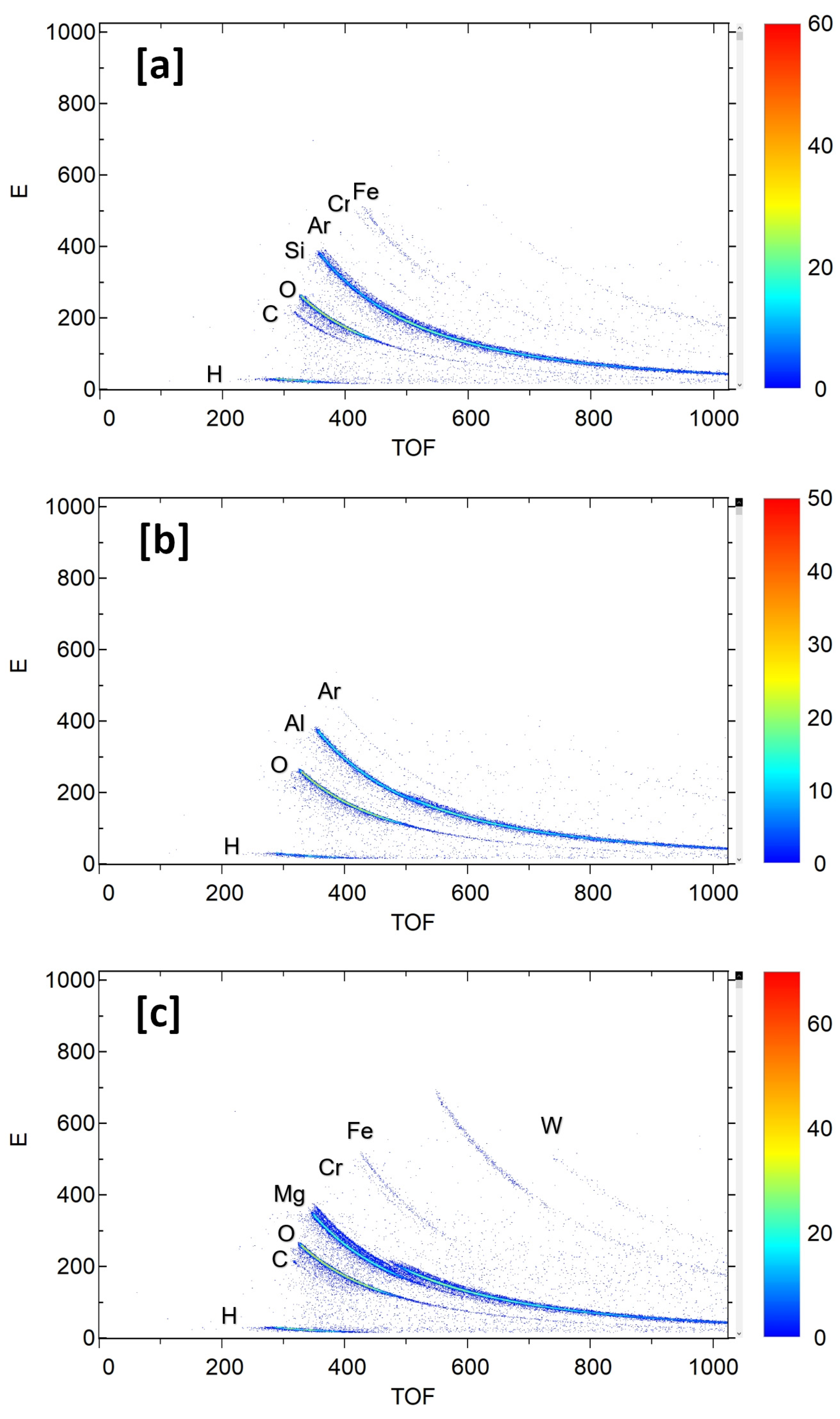
3.1. Elastic Recoil Detection Analysis of Magnetron-Sputtering-Deposited Oxides

The ToF-ERDA measurements provided information about all elements present in the investigated samples simultaneously. In the maps shown in Figure 1, elements can be identified and distinguished by measuring the energy and time of flight of recoils coming out of the sample. Sometimes, as shown for example in Figure 1c, scattered iodine ions from the probing ion beam can also be detected. Therefore, by using this technique, it is possible to determine the elemental composition of thin films with very good mass and depth resolution. The results of the ToF-ERDA measurements we have obtained in this work are presented in Table 3.
The results presented in Table 3 indicate that the produced oxide films are most likely stoichiometric, as expected from used oxide targets. Assuming that hydrogen is bonded within water molecules, it appears that the measured amount of oxygen atoms is only slightly higher than expected, although expected values are still within the error bars. These values are constant throughout the whole film thickness. Very small amounts of elements such as carbon, argon, iron, and chromium (identification of the last two is uncertain) that were found are common for the magnetron sputtering deposition process. Such small amount of impurities, well known residues of the magnetron sputtering process, are not expected to influence the radiation hardness of studied oxide materials [31].

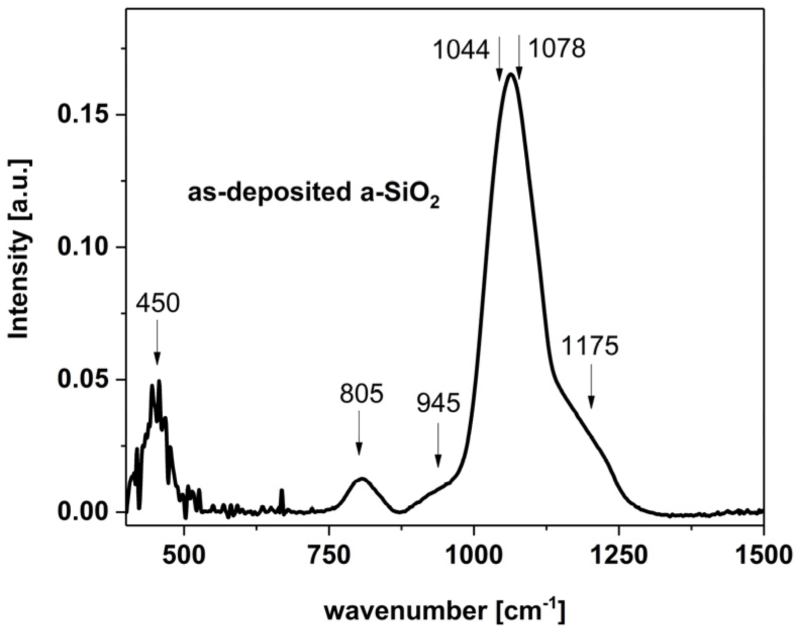
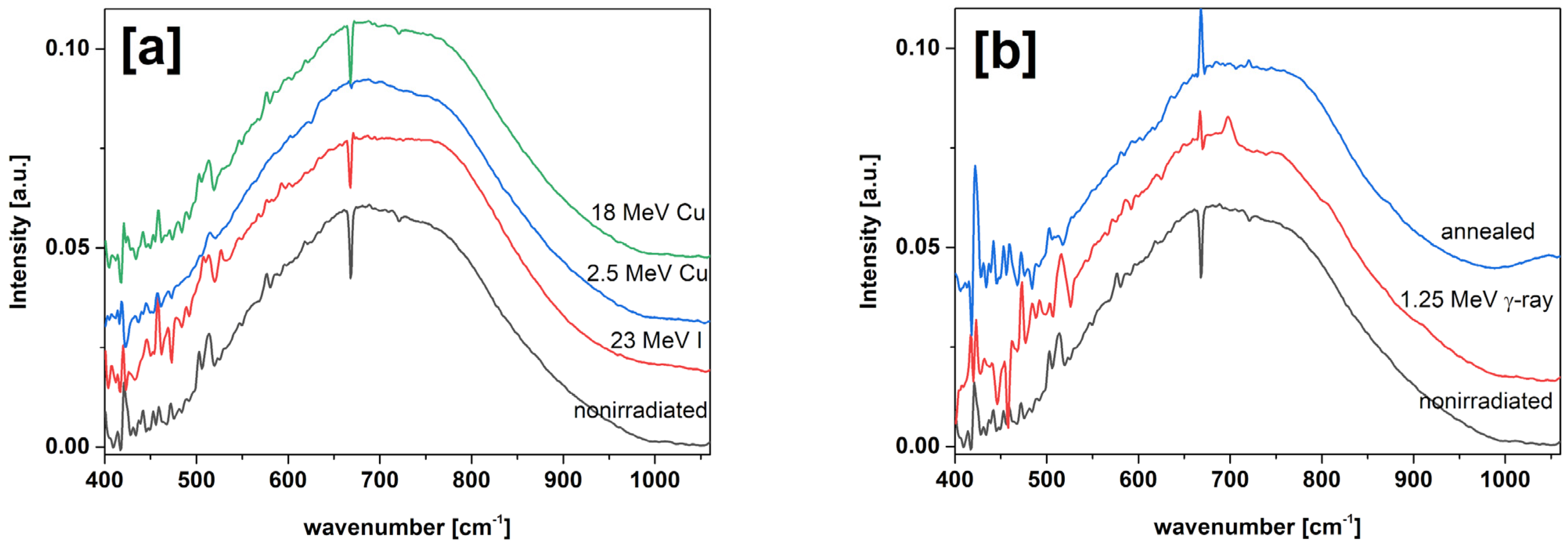
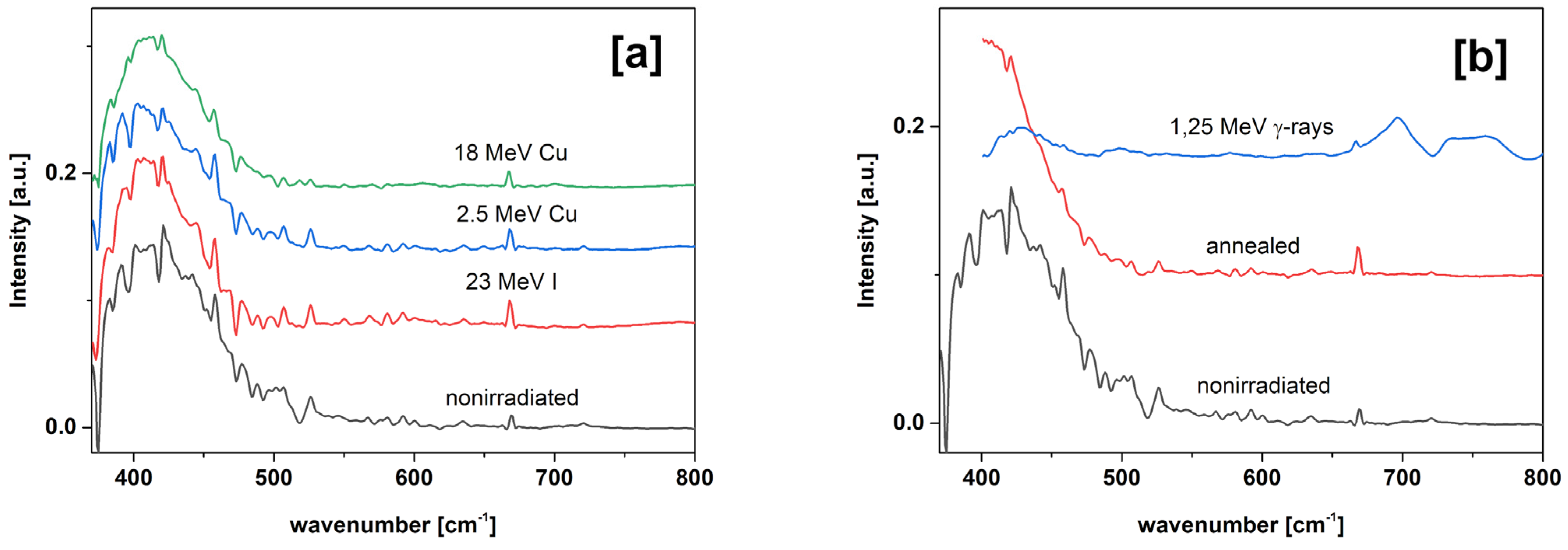
3.2. Comparing Thermally Grown a-SiO2 with Magnetron-Sputtering-Deposited a-SiO2

FTIR spectrum of the as-deposited a-SiO2 sample prepared by magnetron sputtering deposition exhibited six peaks [32,33,34,35], as shown in Figure 2. The most prominent vibrational mode is an asymmetric stretching band, which is not a single peak but a composite of several overlapping contributions, reflecting the variety of local environments, such as different Si-O-Si bond angles and ring structure in the amorphous network. Asymmetric Si-O-Si stretching mode, usually labelled TO3, being the most intense band in the FTIR spectrum of a-SiO2, is composed of two peaks and linked to vibrations of six-membered rings of Si-O tetrahedra. These two peaks are centred at 1044 cm−1 and 1078 cm−1, with the wavenumber difference assigned to different bond angles. The well-known high wavenumber shoulder, located around ~1175 cm−1, is labelled as a TO4 vibration mode and corresponds to the Si-O-Si bonds with smaller bond angles (closer to 120° or even less) in smaller ring structures, such as three-membered rings. The other lower wavenumber shoulder at ~945 cm−1 is due to SiOH (silanol) groups stretching vibrations. Finally, the peak at ~450 cm−1 is due to the Si-O-Si rocking mode and the peak at ~805 cm−1 arises due to the Si-O-Si symmetric stretching mode.
In our previous work [21], we investigated the response of the thermally grown a-SiO2 thin films to ion and gamma-ray irradiation. Here, we used and re-analysed part of that dataset which is relevant to the present study, namely samples irradiated with 23 MeV I and 1.25 MeV gamma-rays. As shown in Figure 3a, iodine ion irradiation produces large changes that are observable using IR spectroscopy, while irradiation with 1.25 MeV gamma-rays up to a dose of 5 MGy introduces only minor changes to the spectrum.
In contrast to this result, iodine ion irradiation does not induce such drastic changes in the IR spectra of a-SiO2 thin films prepared by magnetron sputtering deposition. These spectra, together with spectra obtained from a sample irradiated with 1.25 MeV gamma-rays up to 6 MGy, are shown in Figure 3b. To better understand this surprising result, additional ion irradiation with copper beams (18 MeV Cu and 2.5 MeV Cu) was made, and the obtained spectra were compared with the spectrum from the sample that was annealed at 600 °C for 1 h in vacuum. These spectra show some changes, as shown in Figure 3c, but for their proper evaluation, a detailed analysis was required.
This analysis was carried out in the same manner for all spectra we had at our disposal (i.e., spectra obtained from the old, thermally grown a-SiO2 and new, magnetron-sputtering deposition prepared a-SiO2). The procedure was as follows: the most intense peak is composed of two peaks, one at 1044 cm−1 and another one at 1078 cm−1, which arise from the Si-O-Si asymmetric stretching TO3 mode, as explained in the first paragraph of this section. Observed changes are well-known and redshift of the maxima [15] is attributed to a decrease of 1078 cm−1 peak intensity and an increase of 1044 cm−1 peak intensity [17,20,21]. This occurs because the O-Si-O bond angle decreases from 144° to 129° due to the compaction of silica. The positions of these two well-known peaks are therefore fixed in the analysis, and a fit to the Gauss function was used to evaluate areas of these two overlapped peaks.
In case of thermally grown a-SiO2, irradiation by 23 MeV I beam increases the area of 1044 cm−1 peak and decreases the area of 1078 cm−1 peak, as shown in Figure 3a. These changes evolve rapidly with applied ion fluence, and the kinetics of this process have already been well documented [21]. In contrast to iodine ion irradiations, 1.25 MeV gamma-ray irradiation was found to be much less effective, and doses much larger than 5 MGy were needed to introduce noticeable changes to IR spectra [21].
The magnetron-sputtering-deposited a-SiO2 showed surprisingly little changes in IR spectra when exposed to 23 MeV I irradiation in the same fluence range, as shown in Figure 3b. The total area of the 1044 cm−1 and 1078 cm−1 peaks remains the same, within 5% of the average value, and only slight redshift can be visually observed. This striking difference between spectra shown in Figure 3a,c is associated with different structures of the two a-SiO2 thin films studied here, but slightly different stoichiometric values hinted by ToF-ERDA could play a role too. Another dedicated experiment would be needed to clarify if this is indeed the case. It is important to note that the ratio of 1078 cm−1 and 1044 cm−1 peak areas is ~1–2 for magnetron-sputtering-deposited a-SiO2, for all spectra shown in Figure 3c. In the case of thermally grown a-SiO2, this ratio is ~50 for unirradiated and ~3 for the sample irradiated by the highest fluence of 23 MeV I. This finding suggests that as-prepared magnetron-sputtering-deposited a-SiO2 thin film is already a highly disordered material and further gamma-ray or iodine ion irradiation does not change its initial disordered state much.
The proposed explanation, that magnetron-sputtered a-SiO2 is a highly disordered material, then has to address the visible changes shown in Figure 3e. Upon closer inspection, the similarity of spectra shown in Figure 3c,e is only ostensible. The ratio of 1078 cm−1 and 1044 cm−1 peak areas is ~0.5 for both copper-irradiated samples and the annealed sample. This low value is much less than the previously reported high-fluence limit of ~2 [21] and ~1 [17], which suggests that unusual properties of magnetron-sputtering-deposited a-SiO2 cannot be assigned to a highly disordered state alone. However, we note that in both cases (copper ion irradiation and annealing), a similar state of a thin film was reached, since FTIR spectra show similar features. Besides similar peak area ratios, indicating that copper ion irradiation acts in a similar manner to annealing (and 18 MeV Cu is better in this regard than 2.5 MeV Cu, indicating electronic stopping as annealing counterpart), we also note that the observed maxima redshifted further down to the high-fluence limit of 1044 cm−1 [15].
The observed similarity between copper ion irradiation and thermal annealing opens up a question on the role of electronic stopping in modification of a-SiO2 prepared by magnetron sputtering deposition. The value of electronic stopping clearly exceeds the threshold for ion track formation in a-SiO2, estimated to be around 1.5 keV/nm [21]. A lack of changes in spectra from 23 MeV I-irradiated samples, which have an identical value of electronic stopping power as 18 MeV Cu, should then be assigned to the simultaneous production of damage via nuclear stopping [17] because iodine is much heavier ion than copper, and therefore has a much higher nuclear stopping component (see Table 2). Additional ion irradiation experiments, which should also consider the role of the ion velocity, would be required for a definite answer to this question.
Next, we turn our attention to the remaining two peaks from the studied 900–1300 cm−1 range. The shoulder located at ~1175 cm−1 arises due to TO4 asymmetric stretching positioned in the 1165–1200 cm−1 range [17]. Previously, this peak position and area in FTIR spectra of irradiated thermally grown a-SiO2 were not changing at all, and therefore were not used in the analysis [15,17,21]. At present, we observe radically different behaviour in irradiated a-SiO2 prepared by magnetron sputtering. Again, all spectra shown in Figure 3c are similar and changes to this peak are minor. There is only a slight redshift (<5 cm−1) and an increase in the peak area (<3%) for iodine-irradiated samples when compared to unirradiated and gamma-irradiated samples. On the other hand, spectra shown in Figure 3e are different, as both peak area and width increase, likely due to a wider range of bond angles or change in the mix of ring structures, resulting in the broader peak. These changes are accompanied by a significant redshift (from ~1175 cm−1 down to ~1135 cm−1), indicating changes in the TO4 contribution. Again, the similarity between the effects of copper ion irradiation and thermal annealing indicates an important role of electronic stopping.
The shoulder peak at 945 cm−1 can be observed only in Figure 3c,e. In other words, it is absent in thermally grown a-SiO2 and present only in a-SiO2 samples prepared by magnetron sputtering deposition. This peak arises due to stretching vibrations of SiOH (silanol) groups [36], but is not affected by irradiation. Therefore, we do not study it further here, but it was important to take it into account in the analysis in order to obtain an accurate fitting of the spectra. Similar behaviour is found for other peaks outside the range of interest. There is a peak at 450 cm−1 due to the Si-O-Si rocking mode and another peak at 805 cm−1 due to the Si-O-Si symmetric stretching mode. Both peaks are very insensitive to the ion and gamma-ray irradiation. Since these two peaks do not overlap with any other peak of interest, we do not analyse them here.

3.3. Radiation Hardness of Magnetron-Sputtering-Deposited a-Al2O3 and a-MgO

In Figure 4a, we show the FTIR spectra of a-Al2O3 irradiated with high-energy heavy ions to the highest fluences, and in Figure 4b, the FTIR spectra of a-Al2O3 irradiated with gamma-rays and a-Al2O3 annealed at 600 °C for 1 h in vacuum. In all cases, including a spectrum from a non-irradiated sample, a single, very broad peak (FWHM ~290 cm−1) is found centred at ~700 cm−1. This indicates that the material is completely disordered, with a wide distribution of Al-O bond lengths and coordination geometries. In that case, different Al-O stretching and bending modes, usually found around 430–500, 550–630 cm−1, 650–720 cm−1, and 750–850 cm−1 overlap, and therefore, it is very difficult to resolve their individual contributions [37,38,39,40]. An unusually large width of the peak (FWHM ~290 cm−1) also points to many different bond strengths, which could be due to the low density of a-Al2O3 prepared by magnetron sputtering deposition. Such a broad feature that appears in the FTIR spectrum is therefore indicative of highly disordered amorphous alumina. A feature around 667 cm−1 in all presented FTIR spectra is an artefact caused by atmospheric CO2 absorption. Only in the case of thermal annealing, we observe narrowing of the peak (FWHM ~255 cm−1), indicating some recovery of the material structure. In contrast to a-SiO2, irradiation with an 18 MeV Cu beam does not yield a similar effect, indicating that electronic excitations are not sufficiently intense to induce material recovery in a similar manner. This is in line with previous observations that crystalline Al2O3 is more radiation resistant than SiO2 [12,21]. However, crystalline Al2O3 is very prone to ion track recrystallisation, and this could be a cause for its high radiation hardness. For this reason, dedicated experiments were carried out [41], and it was found that the threshold for ion track formation, when recrystallisation is suppressed, is still much higher than the threshold for ion track formation in quartz SiO2 [42].
Finally, in Figure 5a, we show the FTIR spectra of a-MgO irradiated with high-energy heavy ions to the highest fluences, and in Figure 5b, the FTIR spectra of a-MgO irradiated with gamma-rays and a-MgO annealed at 600 °C for 1 h in vacuum. A broad peak centred around ~415 cm−1 can be observed [43,44]. Due to technical limitations posed by the used spectrometer, the spectra exhibit slightly higher noise at the end of the spectral range, but reliable fitting was still possible. The FTIR spectra from a-MgO samples irradiated by high-energy heavy ions, even up to the highest fluences, do not show much difference compared to the spectrum obtained from the as-prepared sample. We concluded that, similar to the case of high-energy heavy-ion-irradiated a-Al2O3, all of the used ion beams are ineffective in changing the structure of a-MgO because electronic stopping is below the threshold for ion track formation in this material. Again, this is in line with previous observations that both Al2O3 and MgO are very radiation-resistant materials [12].
The spectra shown in Figure 5b show significant differences. The spectrum obtained from the sample that was annealed at 600 °C for 1 h in vacuum shows a moderate redshift of the peak for 20 cm−1. This finding is assigned to relaxation of the as-prepared material (that is usually under compressive and/or tensile stress when deposition is carried out at room temperature) and consequently the observation of transverse optical Mg-O mode in a less strained environment. Surprisingly, the gamma-ray-irradiated sample shows almost complete disappearance of the ~415 cm−1 Mg-O stretching peak (peak position is shifted to 430 cm−1, peak area decreases ~15×, and FWHM is reduced by 50%). Apparently, this type of irradiation strongly disrupts Mg-O bonds, but currently, the underlying cause remains unknown to us. This finding is in stark contrast to the high-energy heavy ion irradiation which preserves short-range order, i.e., for which the Mg-O stretch remains FTIR-active. Hence, the important takeaway here is that high-energy heavy ion irradiation cannot always be used as a proxy to emulate gamma-ray irradiation-induced material changes [21], but should be carefully investigated when this approach is feasible for a given material.

4. Conclusions

In this work, we present the extraordinary radiation hardness of amorphous oxide thin films (a-SiO2, a-Al2O3 and a-MgO) prepared by the magnetron sputtering deposition. The results of the IR spectroscopy indicate that high levels of disorder already present in as-prepared samples effectively inhibit further damage build-up when exposed to high levels of irradiation, both in the case of high-energy heavy ions and gamma-ray irradiation. In some cases, high-energy heavy ion irradiation (such as 18 MeV Cu in a-SiO2) can actually improve the structure of thin films, in a similar manner as classical thermal annealing. In the future, more work is needed to understand what is the role of stoichiometry in the radiation hardness of studied amorphous oxide thin films, in particular when sub-oxide films can be successfully prepared via magnetron sputtering deposition [45,46]. Also, of great interest is to understand to what extent high-energy heavy ion irradiation can be used as a proxy for the simulation of gamma-ray irradiation-induced changes, which should be studied systematically for the a-MgO system. Finally, the use of ion beams in selectively modifying amorphous films can offer an alternative route to tailor material properties for which more complex magnetron sputtering deposition procedures are now required [47].

Author Contributions

Conceptualisation, M.Š. and M.K.; Formal analysis, M.Š., Z.S. and M.K.; Funding acquisition, M.K.; Investigation, M.Š.; M.M. (Marija Majer), Z.S., M.M. (Maja Mičetić), Ž.K. and M.K.; Methodology, M.Š., Z.S. and M.K.; Project administration, M.K.; Resources, M.K.; Validation, M.Š., Z.S. and M.K.; Visualisation, M.Š. and Z.S.; Writing—original draft, M.K.; Writing—review and editing, M.Š., M.M. (Marija Majer), Z.S., M.M. (Maja Mičetić), Ž.K. and M.K. All authors have read and agreed to the published version of the manuscript.

Funding

This work was supported by the Croatian Science Foundation (HRZZ pr. no. 5023). The authors acknowledge support from the European Regional Development Fund for the ‘Center of Excellence for Advanced Materials and Sensing Devices’ (grant no. KK.01.1.1.01.0 0 01).

Institutional Review Board Statement

Not applicable.

Informed Consent Statement

Not applicable.

Data Availability Statement

The raw data supporting the conclusions of this article will be made available by the authors on request.

Conflicts of Interest

The authors declare no conflicts of interest.

References

  1. Toulemonde, M.; Assmann, W.; Dufour, C.; Meftah, A.; Trautmann, C. Nanometric transformation of the matter by short and intense electronic excitation: Experimental data versus inelastic thermal spike model. Nucl. Instrum. Methods Phys. Res. Sect. B Beam Interact. Mater. At. 2012, 277, 28. [Google Scholar] [CrossRef]
  2. Agulló-López, F.; Climent-Font, A.; Muñoz-Martín, Á.; Olivares, J.; Zucchiatti, A. Ion beam modification of dielectric materials in the electronic excitation regime: Cumulative and exciton models. Prog. Mater. Sci. 2016, 76, 1. [Google Scholar] [CrossRef]
  3. Klaumünzer, S. Ion Tracks in quartz and vitreous silica. Nucl. Instrum. Methods Phys. Res. Sect. B Beam Interact. Mater. At. 2004, 225, 136. [Google Scholar] [CrossRef]
  4. Aumayr, F.; Facsko, S.; El-Said, A.S.; Trautmann, C.; Schleberger, M. Single ion induced surface nanostructures: A comparison between slow highly charged and swift heavy ions. J. Phys. Condens. Matter. 2011, 23, 393001. [Google Scholar] [CrossRef]
  5. Weber, W.J.; Ewing, R.C.; Catlow, C.R.A.; de la Rubia, T.D.; Hobbs, L.W.; Kinoshita, C.; Matzke, H.J.; Motta, A.T.; Nastasi, M.; Salje, E.K.H.; et al. Radiation effects in crystalline ceramics for the immobilization of high-level nuclear waste and plutonium. J. Mater. Res. 1998, 13, 1434. [Google Scholar] [CrossRef]
  6. Mir, A.H.; Peuget, S. Using external ion irradiations for simulating self-irradiation damage in nuclear waste glasses. State of the art, recommendations and prospects. J. Nucl. Mater. 2020, 539, 152246. [Google Scholar] [CrossRef]
  7. Akcöltekin, S.; Akcöltekin, E.; Roll, T.; Lebius, H.; Schleberger, M. Patterning of insulating surfaces by electronic excitation. Nucl. Instrum. Methods Phys. Res. Sect. B Beam Interact. Mater. At. 2009, 267, 1386. [Google Scholar] [CrossRef]
  8. Meftah, A.; Brisard, F.; Constantini, J.M.; Dooryhee, E.; Hage-Ali, M.; Hervieu, M.; Stoquert, J.P.; Studer, F.; Toulemonde, M. Track formation in SiO2 quartz and the thermal-spike mechanism. Phys. Rev. B 1994, 49, 12457. [Google Scholar] [CrossRef]
  9. Toulemonde, M.; Ramos, S.M.M.; Bernas, H.; Clerc, C.; Canut, B.; Chaumont, J.; Trautmann, C. MeV gold irradiation induced damage in a quartz: Competition between nuclear and electronic stopping. Nucl. Instrum. Methods Phys. Res. Sect. B Beam Interact. Mater. At. 2001, 178, 331. [Google Scholar] [CrossRef]
  10. Peña-Rodríguez, O.; Manzano-Santamaría, J.; Rivera, A.; García, G.; Olivares, J.; Agulló-López, F. Kinetics of amorphization induced by swift heavy ions in alpha-quartz. J. Nucl. Mater. 2012, 430, 125. [Google Scholar] [CrossRef]
  11. Luketić, K.T.; Hanžek, J.; Mihalcea, C.G.; Dubček, P.; Gajović, A.; Siketić, Z.; Jakšić, M.; Ghica, C.; Karlušić, M. Charge State Effects in Swift-Heavy-Ion-Irradiated Nanomaterials. Crystals 2022, 12, 865. [Google Scholar] [CrossRef]
  12. Karlušić, M.; Rymzhanov, R.A.; O’Connell, J.H.; Bröckers, L.; Luketić, K.T.; Siketić, Z.; Fazinić, S.; Dubček, P.; Jakšić, M.; Provatas, G.; et al. Mechanisms of surface nanostructuring of Al2O3 and MgO by grazing incidence irradiation with swift heavy ions. Surf. Interf. 2021, 27, 101508. [Google Scholar] [CrossRef]
  13. Hanžek, J.; Dubček, P.; Fazinić, S.; Luketić, K.T.; Karlušić, M. High-Energy Heavy Ion Irradiation of Al2O3, MgO and CaF2. Materials 2022, 15, 2110. [Google Scholar] [CrossRef] [PubMed]
  14. Toulemonde, M.; Dufour, C.; Paumier, E. Transient thermal process after a high-energy heavy-ion irradiation of amorphous metals and semiconductors. Phys. Rev. B 1992, 46, 14362. [Google Scholar] [CrossRef]
  15. Awazu, K.; Ishii, S.; Shima, K.; Roorda, S.; Brebner, J.L. Structure of latent tracks created by swift heavy-ion bombardment of amorphous SiO2. Phys. Rev. 2000, 62, 3689. [Google Scholar] [CrossRef]
  16. Kluth, P.; Schnohr, C.S.; Pakarinen, O.H.; Djurabekova, F.; Sprouster, D.J.; Giulian, R.; Ridgway, M.C.; Byrne, A.P.; Trautmann, C.; Cookson, D.J.; et al. Fine Structure in Swift Heavy Ion Tracks in Amorphous SiO2. Phys. Rev. Lett. 2008, 101, 175503. [Google Scholar] [CrossRef]
  17. Toulemonde, M.; Weber, W.J.; Li, G.; Shutthanandan, V.; Kluth, P.; Yang, T.; Wang, Y.; Zhang, Y. Synergy of nuclear and electronic energy losses in ion-irradiation processes: The case of vitreous silicon dioxide. Phys. Rev. B 2011, 83, 054106. [Google Scholar] [CrossRef]
  18. Kluth, P.; Pakarinen, O.H.; Djurabekova, F.; Giulian, R.; Ridgway, M.C.; Byrne, A.P.; Nordlund, K. Nanoscale density fluctuations in swift heavy ion irradiated amorphous SiO2. J. Appl. Phys. 2011, 110, 123520. [Google Scholar] [CrossRef]
  19. Rotaru, C.; Pawlak, F.; Khalfaoui, N.; Dufour, C.; Perrière, J.; Laurent, A.; Stoquert, J.P.; Lebius, H.; Toulemonde, M. Track formation in two amorphous insulators, vitreous silica and diamond like carbon: Experimental observations and description by the inelastic thermal spike model. Nucl. Instrum. Methods Phys. Res. Sect. B Beam Interact. Mater. At. 2012, 272, 9. [Google Scholar] [CrossRef]
  20. Benyagoub, A.; Toulemonde, M. Ion tracks in amorphous silica. J. Mater. Res. 2015, 30, 1529. [Google Scholar] [CrossRef]
  21. Karlušić, M.; Škrabić, M.; Majer, M.; Buljan, M.; Skuratov, V.A.; Jung, H.K.; Gamulin, O.; Jakšić, M. Infrared spectroscopy of ion tracks in amorphous SiO2 and comparison to gamma irradiation induced changes. J. Nucl. Mater. 2019, 514, 74. [Google Scholar] [CrossRef]
  22. Buljan, M.; Karlušić, M.; Bogdanović-Radović, I.; Jakšić, M.; Salamon, K.; Bernstorff, S.; Radić, N. Determination of ion track radii in amorphous matrices via formation of nano-clusters by ion-beam irradiation. Appl. Phys. Lett. 2012, 101, 103112. [Google Scholar] [CrossRef]
  23. Carvalho, A.M.J.F.; Marinoni, M.; Touboul, A.D.; Guasch, C.; Lebius, H.; Ramonda, M.; Bonnet, J.; Saigne, F. Discontinuous ion tracks on silicon oxide on silicon surfaces after grazing-angle heavy ion irradiation. Appl. Phys. Lett. 2007, 90, 073116. [Google Scholar] [CrossRef]
  24. Carvalho, A.M.J.F.; Touboul, A.D.; Marinoni, M.; Ramonda, M.; Guasch, C.; Saigne, F.; Bonnet, J.; Gasiot, J. Oxide thickness dependence of swift heavy ion-induced surface tracks formation in silicon dioxide on silicon structures at grazing incidence. J. Appl. Phys. 2007, 102, 124306. [Google Scholar] [CrossRef]
  25. Carvalho, A.M.J.F.; Touboul, A.D.; Marinoni, M.; Carlotti, J.-F.; Guasch, C.; Ramonda, M.; Lebius, H.; Saigne, F.; Bonnet, J. SiO2–Si under swift heavy ion irradiation: A comparison between normal and grazing incidence features. Nucl. Instrum. Methods Phys. Res. Sect. B Beam Interact. Mater. At. 2008, 266, 2981. [Google Scholar] [CrossRef]
  26. Karlušić, M.; Mičetić, M.; Kresić, M.; Jakšić, M.; Šantić, B.; Bogdanović-Radović, I.; Bernstorff, S.; Lebius, H.; Ban-d’Etat, B.; Rožman, K.Ž.; et al. Nanopatterning surfaces by grazing incidence swift heavy ion irradiation. Appl. Surf. Sci. 2021, 541, 148467. [Google Scholar] [CrossRef]
  27. Arstila, K.; Julin, J.; Laitinen, M.I.; Aalto, J.; Konu, T.; Kärkkäinen, S.; Rahkonen, S.; Raunio, M.; Itkonen, J.; Santanen, J.P.; et al. Potku—New analysis software for heavy ion elastic recoil detection analysis. Nucl. Instr. Meth. Phys. Res. Sect. B Beam Interact. Mater. At. 2014, 331, 34. [Google Scholar] [CrossRef]
  28. Siketić, Z.; Bogdanović-Radović, I.; Jakšić, M. Development of a time-of-flight spectrometer at the Ruđer Bošković Institute in Zagreb. Nucl. Instr. Meth. Phys. Res. B Beam Interact. Mater. At. 2008, 266, 1328. [Google Scholar] [CrossRef]
  29. Ziegler, J.F.; Ziegler, M.D.; Biersack, J.P. SRIM—the stopping and range of ions in the matter (2010). Nucl. Instr. Meth. Phys. Res. B Beam Interact. Mater. At. 2010, 268, 1818. [Google Scholar] [CrossRef]
  30. Majer, M.; Pasariček, L.; Knežević, Ž. Dose mapping of the 60Co gamma irradiation facility and a real irradiated product—Measurements and Monte Carlo simulation. Radiat. Phys. Chem. 2024, 214, 111280. [Google Scholar] [CrossRef]
  31. Ishikawa, N.; Fujimura, Y.; Kondo, K.; Szabo, G.L.; Wilhelm, R.A.; Ogawa, H.; Taguchi, T. Surface nanostructures on Nb-doped SrTiO3 irradiated with swift heavy ions at grazing incidence. Nanotechnology 2022, 33, 235303. [Google Scholar] [CrossRef] [PubMed]
  32. Pai, P.G.; Chao, S.S.; Takagi, Y.; Lucovsky, G. Infrared spectroscopic study of SiOx films produced by plasma enhanced chemical vapor deposition. J. Vac. Sci. Techn. A 1986, 4, 689. [Google Scholar] [CrossRef]
  33. Herth, E.; Zeggari, R.; Rauch, J.-Y.; Remy-Martin, F.; Boireau, W. Investigation of amorphous SiOx layer on gold surface for Surface Plasmon Resonance measurements. Microel. Eng. 2016, 163, 43. [Google Scholar] [CrossRef]
  34. Sanaeishoar, H.; Sabbaghan, M.; Mohave, F. Synthesis and characterization of micro-mesoporous MCM-41 using various ionic liquids as co-templates. Micropor. Mesopor. Mater. 2015, 217, 219. [Google Scholar] [CrossRef]
  35. Ellerbrock, R.; Stein, M.; Schaller, J. Comparing amorphous silica, short-range-ordered silicates and silicic acid species by FTIR. Sci. Rep. 2022, 12, 11708. [Google Scholar] [CrossRef] [PubMed]
  36. Innocenzi, P. Infrared spectroscopy of sol–gel derived silica-based films: A spectra-microstructure overview. J. Non Cryst. Solids 2003, 316, 309. [Google Scholar] [CrossRef]
  37. Giacomazzi, L.; Shcheblanov, N.S.; Povarnitsyn, M.E.; Li, Y.; Mavrič, A.; Zupančić, B.; Grdadolnik, J.; Pasquarello, A. Infrared spectra in amorphous alumina: A combined ab initio and experimental study. Phys. Rev. Mater. 2023, 7, 045604. [Google Scholar] [CrossRef]
  38. Rutkowska, I.; Marchewka, J.; Jeleń, P.; Odziomek, M.; Korpyś, M.; Paczkowska, J.; Sitarz, M. Chemical and Structural Characterization of Amorphous and Crystalline Alumina Obtained by Alternative Sol–Gel Preparation Routes. Materials 2021, 14, 1761. [Google Scholar] [CrossRef]
  39. Colomban, P. Structure of oxide gels and glasses by infrared and Rarnan scattering. J. Mater. Sci. 1989, 24, 3002. [Google Scholar] [CrossRef]
  40. Dasgupta, A.; Chowdhuri, A.R.; Takoudis, C.G. Metalorganic chemical vapor deposition of aluminum oxide on silicon nitride. Mat. Res. Soc. Symp. Proc. 2003, 751, Z3–Z45. [Google Scholar] [CrossRef]
  41. Aruga, T.; Katano, Y.; Ohmichi, T.; Okayasu, S.; Kazumata, Y. Amorphization behaviors in polycrystalline alumina irradiated with energetic iodine ions. Nucl. Instr. Meth. Phys. Res. B Beam Interact. Mater. At. 2000, 166, 913. [Google Scholar] [CrossRef]
  42. Szenes, G. Ion-induced amorphization in ceramic materials. J. Nucl. Mater. 2005, 336, 81. [Google Scholar] [CrossRef]
  43. Mohandes, F.; Davar, F.; Salavati-Niasari, M. Magnesium oxide nanocrystals via thermal decomposition of magnesium oxalate. J. Phys. Chem. Solids 2010, 71, 1623. [Google Scholar] [CrossRef]
  44. Thoms, H.; Epple, M.; Reller, A. The thermal decomposition of magnesium alcoholates to magnesia (MgO): Studies by IR and thermal analysis. Solid State Ion. 1997, 101, 79–84. [Google Scholar] [CrossRef]
  45. Arnoldbik, W.M.; Tomozeiu, N.; van Hattum, E.D.; Lof, R.W.; Vredenberg, A.M.; Habraken, F.H.P.M. High-energy ion-beam-induced phase separation in SiOx films. Phys. Rev. B 2005, 71, 125329. [Google Scholar] [CrossRef]
  46. Wong, M.-S.; Lin, Y.-J.; Pylnev, M.; Kang, W.-Z. Processing, structure and properties of reactively sputtered films of titanium dioxide and suboxides. Thin Solid Film. 2019, 688, 137351. [Google Scholar] [CrossRef]
  47. Politano, G.G. Optical Properties of Graphene Nanoplatelets on Amorphous Germanium Substrates. Molecules 2024, 29, 4089. [Google Scholar] [CrossRef]
Figure 1. ToF-ERDA maps obtained from the analysis of (a) a-SiO2, (b) a-Al2O3, and (c) a-MgO.
Applsci 15 07067 g001
Figure 2. FTIR spectrum of the as-deposited a-SiO2 prepared by magnetron sputtering deposition.
Applsci 15 07067 g002
Figure 3. FTIR spectra obtained from 23 MeV I and 1.25 MeV gamma-ray-irradiated (a) thermally grown a-SiO2, (c) magnetron-sputtering-deposited a-SiO2, and (e) additional IR spectra from annealed and 18 MeV Cu and 2.5 MeV Cu-irradiated magnetron-sputtering-deposited a-SiO2. Exemplary fits of (b) unirradiated thermally grown a-SiO2, (d) unirradiated a-SiO2 prepared by magnetron sputtering deposition, and (f) a-SiO2 irradiated by 18 MeV Cu to a fluence of 3 × 10¹³ ions/cm2.
Applsci 15 07067 g003
Figure 4. FTIR spectra of (a) high-energy heavy-ion-irradiated a-Al2O3 and (b) gamma-ray-irradiated and annealed a-Al2O3.
Applsci 15 07067 g004
Figure 5. FTIR spectra of (a) high-energy heavy-ion-irradiated a-MgO and (b) gamma-ray-irradiated and annealed a-MgO.
Applsci 15 07067 g005
Table 1. Magnetron sputtering deposition parameters used in this work.
MaterialPower (W)Time (s)Nominal Thickness (nm)
SiO21506.000150
Al2O319014.400150
MgO14036.000180
SiO2 + Al2O363 + 1907.200150
Table 2. High-energy heavy ion irradiation parameters calculated by the SRIM code [29].
MaterialIon BeamElectronic Stopping (keV/µg/cm2)Nuclear Stopping (keV/µg/cm2)
SiO223 MeV I23.701.17
18 MeV Cu23.530.28
2.5 MeV Cu5.741.19
Al2O323 MeV I22.731.13
18 MeV Cu22.730.27
2.5 MeV Cu5.581.16
MgO23 MeV I23.001.16
18 MeV Cu23.540.28
2.5 MeV Cu5.741.18
Table 3. Elemental composition of oxide thin films determined by ToF-ERDA.
Nominal
Composition
A-SiO2A-Al2O3A-MgO
Measured
composition
H          8.7 ± 0.6
C          2.0 ± 0.2
O          60 ± 4
Si          27 ± 1
Ar         0.05 ± 0.02
Cr(?)     0.18 ± 0.03
Fe(?)     0.68 ± 0.07
H     3.9 ± 0.3
O     59 ± 4
Al    36 ± 2
Ar    0.23 ± 0.03
H          6.7 ± 0.5
O          50 ± 3
Mg        42 ± 2
Cr(?)     0.16 ± 0.02
Fe(?)     0.4 ± 0.04
W(?)     0.083 ± 0.007
Thickness
(1015 at/cm2)
141318571750
Disclaimer/Publisher’s Note: The statements, opinions and data contained in all publications are solely those of the individual author(s) and contributor(s) and not of MDPI and/or the editor(s). MDPI and/or the editor(s) disclaim responsibility for any injury to people or property resulting from any ideas, methods, instructions or products referred to in the content.

