
Defect Detection and Error Source Tracing in Laser Marking of Silicon Wafers with Machine Learning

Abstract
1. Introduction
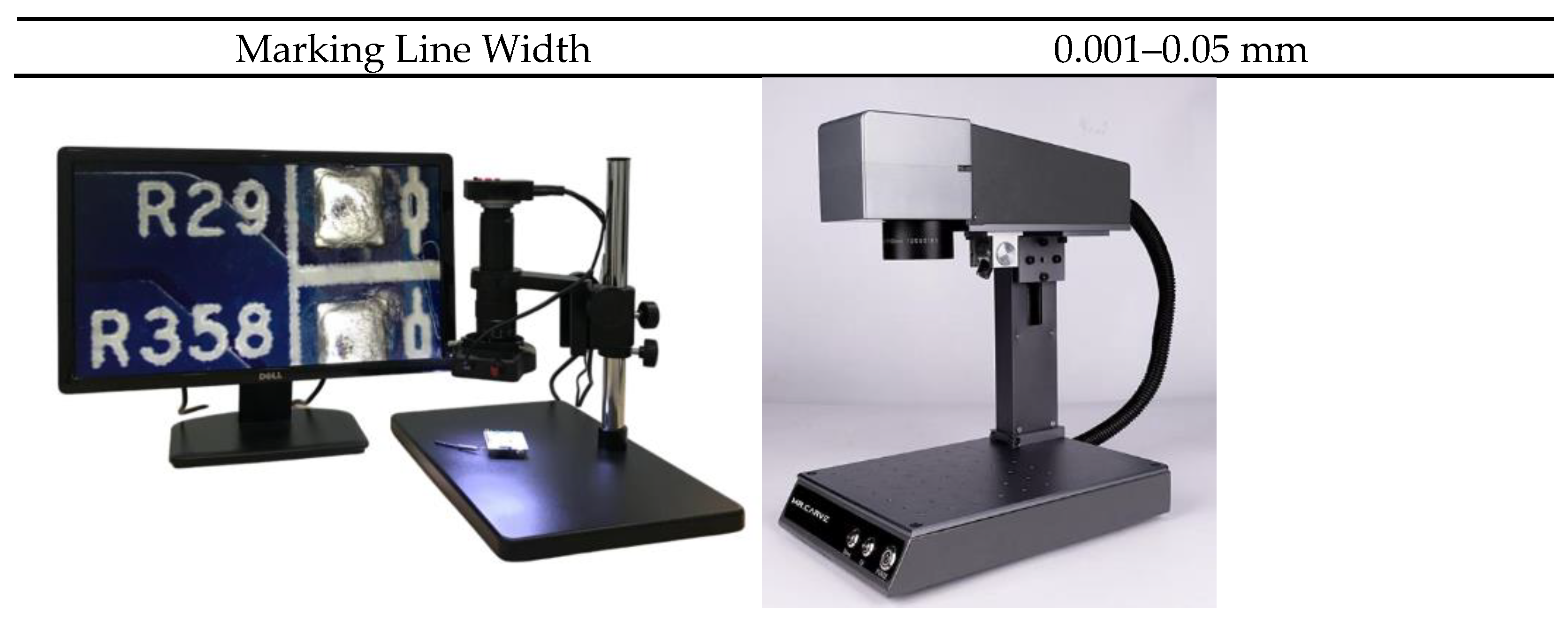
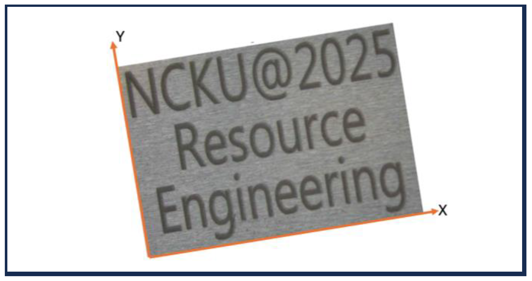
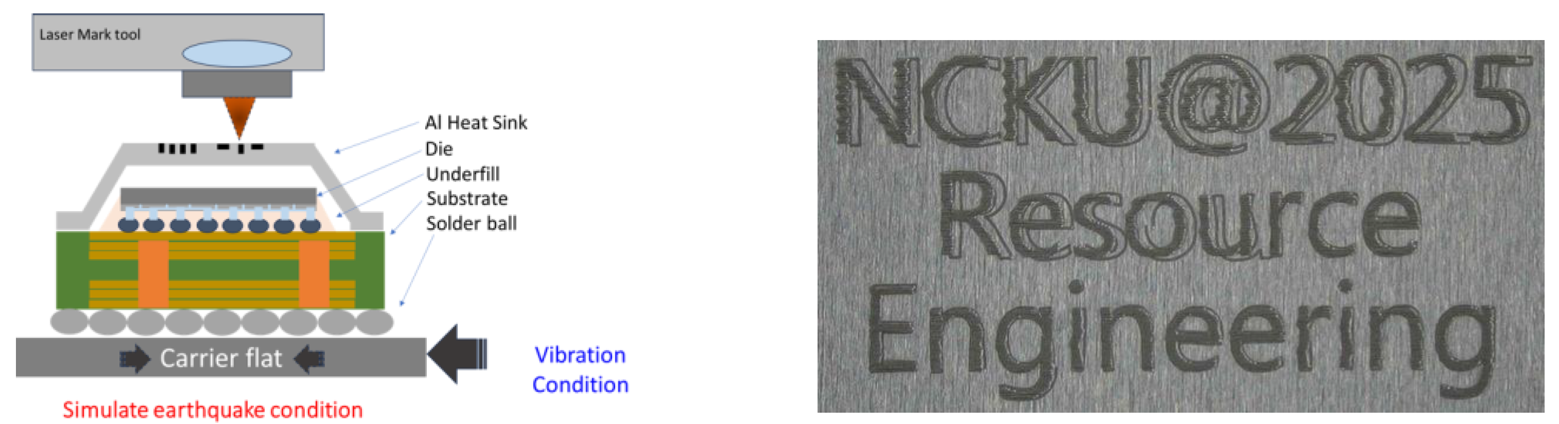
2. Materials and Methods
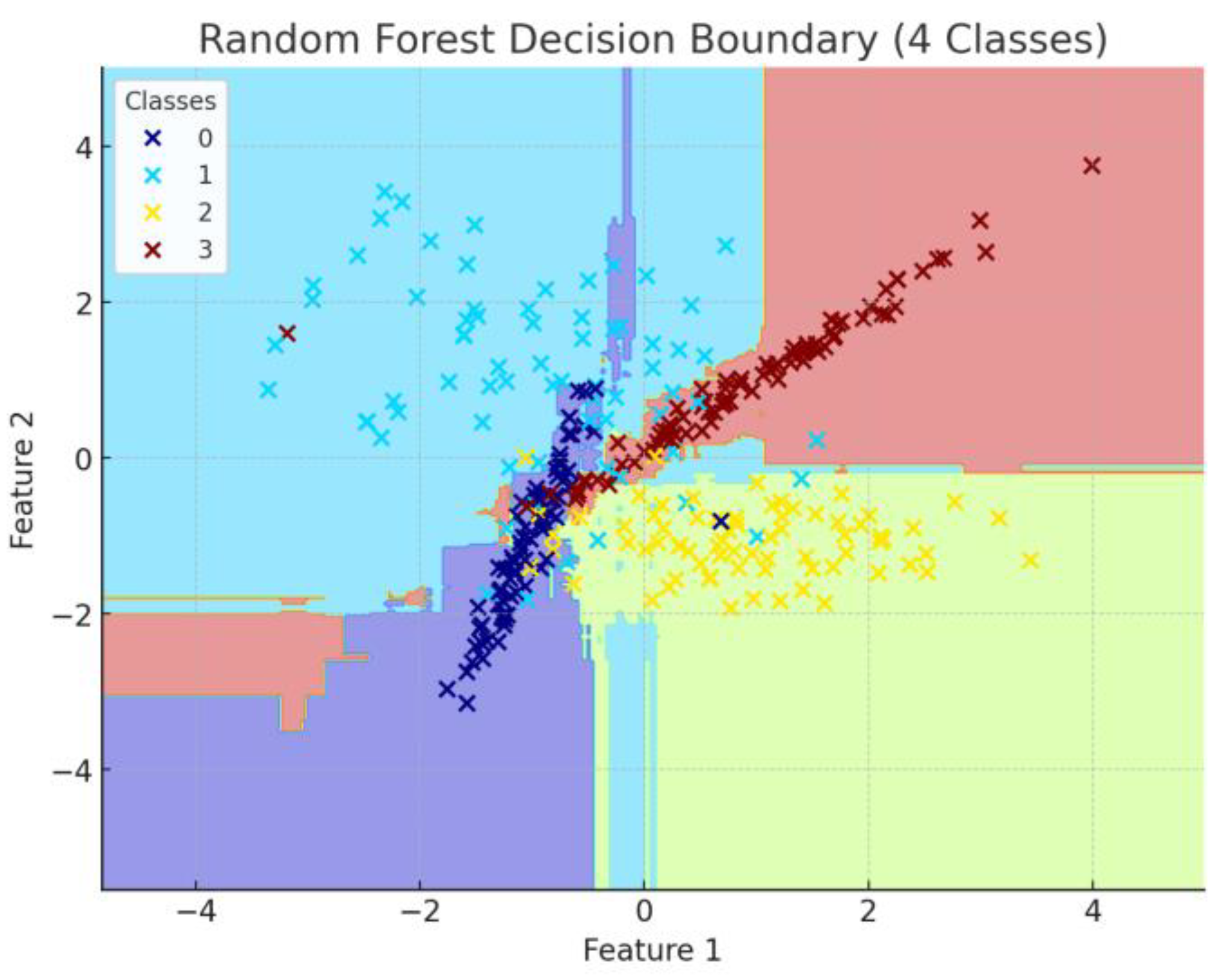
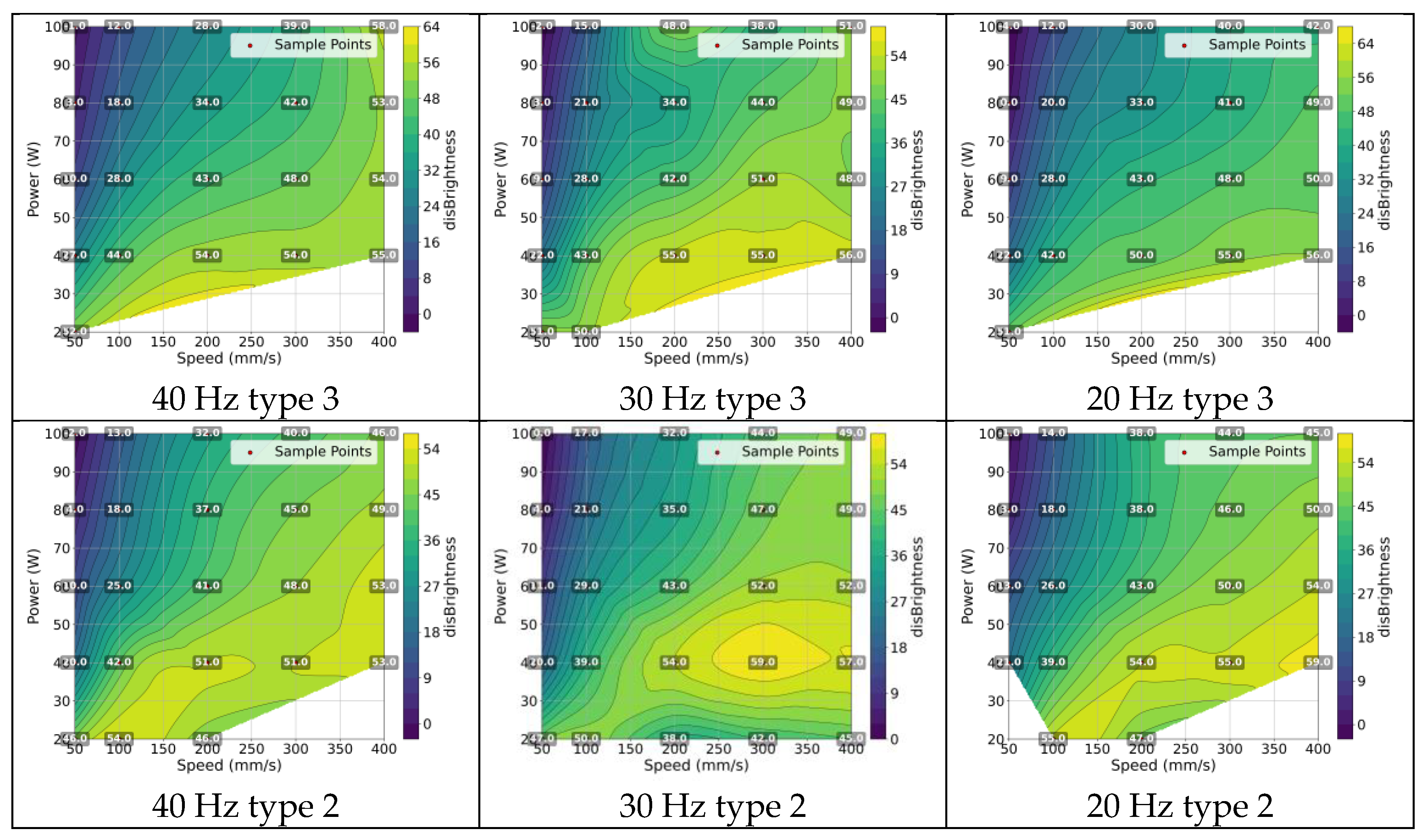
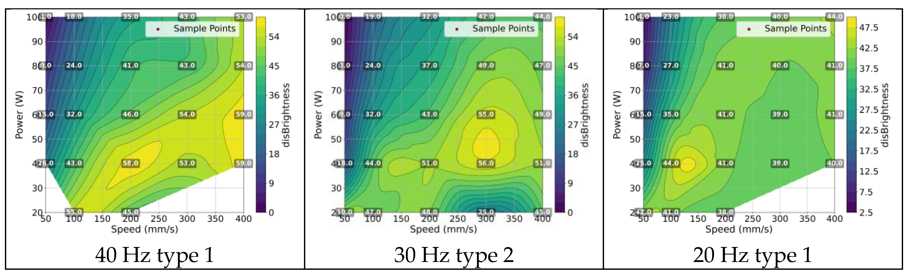
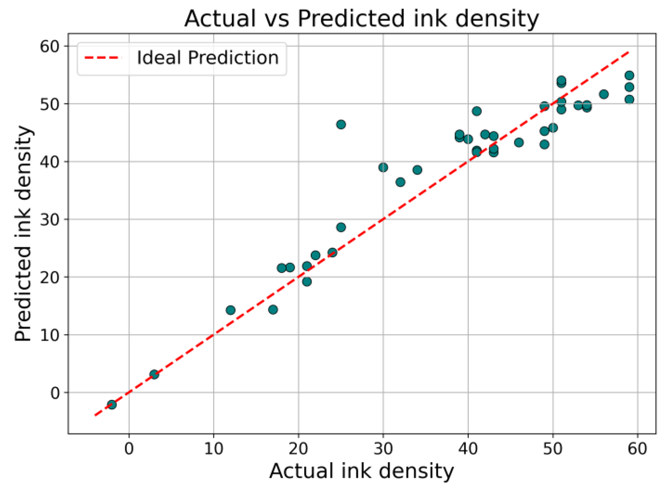
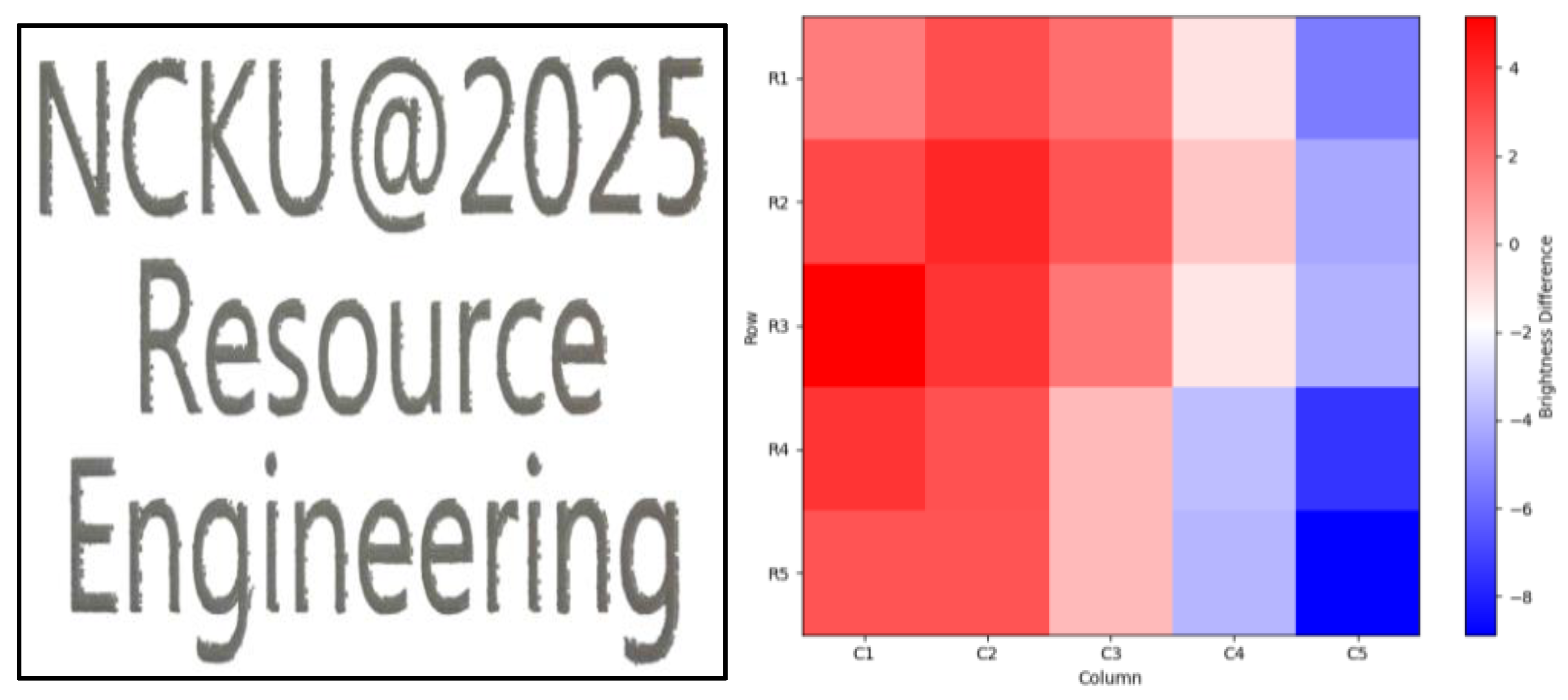
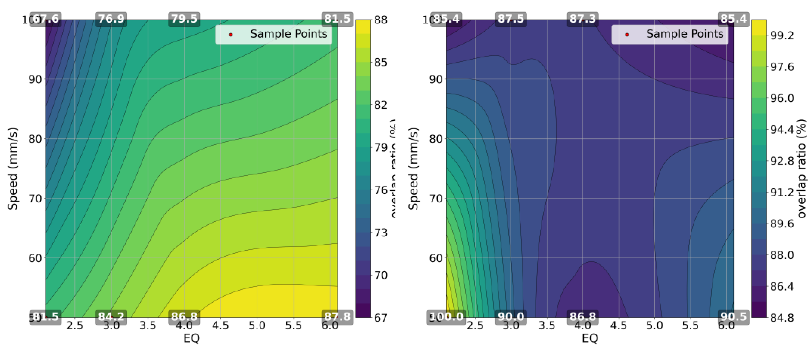
3. Results
4. Discussion
Author Contributions
Funding
Informed Consent Statement
Data Availability Statement
Conflicts of Interest
References
- Lazov, L.; Deneva, H.; Narica, P. Laser Marking Methods. ETR 2015, 1, 108–115. [Google Scholar] [CrossRef]
- Fu, Y.; Downey, A.R.J.; Yuan, L.; Zhang, T.; Pratt, A.; Balogun, Y. Machine learning algorithms for defect detection in metal laser-based additive manufacturing: A review. J. Manuf. Process. 2022, 75, 693–710. [Google Scholar] [CrossRef]
- Du, Y.; Chen, J.; Zhou, H.; Yang, X.; Wang, Z.; Zhang, J.; Shi, Y.; Chen, X.; Zheng, X. An automated optical inspection (AOI) platform for three-dimensional (3D) defects detection on glass micro-optical components (GMOC). Opt. Commun. 2023, 545, 129736. [Google Scholar] [CrossRef]
- Qu, D.; Zhou, Z.; Li, Z.; Ding, R.; Jin, W.; Luo, H.; Xiong, W. Wafer Eccentricity Deviation Measurement Method Based on Line-Scanning Chromatic Confocal 3D Profiler. Photonics 2023, 10, 398. [Google Scholar] [CrossRef]
- de la Rosa, F.L.; Sánchez-Reolid, R.; Gómez-Sirvent, J.L.; Morales, R.; Fernández-Caballero, A. A Review on Machine and Deep Learning for Semiconductor Defect Classification in Scanning Electron Microscope Images. Appl. Sci. 2021, 11, 9508. [Google Scholar] [CrossRef]
- Wang, X.; Zeng, Y.; Han, X.; Xu, M.; Dai, S. Imaging features of different defects in metals using laser ultrasonic techniques. Opt. Laser Technol. 2023, 158 Pt A, 108785. [Google Scholar] [CrossRef]
- Webster, P.J.L.; Wright, L.G.; Mortimer, K.D.; Leung, B.Y.; Yu, J.X.Z.; Fraser, J.M. Automatic real-time guidance of laser machining with inline coherent imaging. J. Laser Appl. 2011, 23, 022001. [Google Scholar] [CrossRef]
- Ding, Y.; Liu, L.; Wang, C.; Li, C.; Lin, N.; Niu, S.; Han, Z.; Duan, J. Bioinspired Near-Full Transmittance MgF2 Window for Infrared Detection in Extremely Complex Environments. Am. Chem. Soc. 2023, 25, 30985–30997. [Google Scholar] [CrossRef] [PubMed]
- Jia, X.; Lin, J.; Li, Z.; Wang, C.; Li, K.; Wang, C.; Duan, J. Continuous wave laser ablation of alumina ceramics under long focusing condition. J. Manuf. Process. 2025, 134, 530–546. [Google Scholar] [CrossRef]
- Nazzal, D.; El-Nashar, A. Survey of research in modeling conveyor-based automated material handling systems in wafer fabs. In Proceedings of the 2007 Winter Simulation Conference, Washington, DC, USA, 9–12 December 2007; pp. 1781–1788. [Google Scholar] [CrossRef]
- Ahmed, Y.S.; Amorim, F.L. Advances in Computer Numerical Control Geometric Error Compensation: Integrating AI and On-Machine Technologies for Ultra- Precision Manufacturing. Machines 2025, 13, 140. [Google Scholar] [CrossRef]
- Hsu, F.-H.; Shen, C.-A. The Design and Implementation of an Embedded Real-Time Automated IC Marking Inspection System. IEEE Trans. Semicond. Manuf. 2019, 32, 112–120. [Google Scholar] [CrossRef]
- Tulbure, A.-A.; Tulbure, A.-A.; Dulf, E.-H. A review on modern defect detection models using DCNNs—Deep convolutional neural networks. J. Adv. Res. 2022, 35, 33–48. [Google Scholar] [CrossRef] [PubMed]
- Zheng, Y.; Chee, K.-W.A. Advanced Techniques in Semiconductor Defect Detection and Classification: Overview of Current Technologies and Future Trends in AI/ML Integration. In Proceedings of the 2024 World Rehabilitation Robot Convention (WRRC), Shanghai, China; 2024; pp. 1–5. [Google Scholar] [CrossRef]
- Wang, C.-H.; Kuo, W.; Bensmail, H. Detection and classification of defect patterns on semiconductor wafers. IIE Trans. 2006, 38, 1059–1068. [Google Scholar] [CrossRef]
- More, A.S.; Rana, D.P. Review of random forest classification techniques to resolve data imbalance. In Proceedings of the 2017 1st International Conference on Intelligent Systems and Information Management (ICISIM), Aurangabad, India; 2017; pp. 72–78. [Google Scholar] [CrossRef]
- Agrawal, H.; Desai, K. Canny Edge Detection: A Comprehensive Review. Int. J. Tech. Res. Sci. 2024, 9, 27–35. [Google Scholar] [CrossRef] [PubMed]


| Item | Specification |
|---|---|
| Frame Rate | 60 fps |
| Image Resolution | 1920 × 1080 pixel |
| Sensor | 1/2.8” SONY |
| Pixel Size | 2.9 × 2.9 μm |
| Picture | SD card 38M |
| Light | Ring Light 52D LED |
| Measurement | Via software |
| Output Interface | HDMI + USB |
| Laser Power | 10 W |
|---|---|
| Repeat Accuracy | ≤0.001 mm |
| Marking Depth | 0.012–0.2 mm |
| Marking Precision | ≤0.001 mm |
| Marking Speed | ≤10,000 mm/s |
| Laser Wavelength | 1064 nm |
| Marking Area | 70 × 70 mm |
| Marking Line Width | 0.001–0.05 mm |
| Product | ||
|---|---|---|
| Result | 570 | 9 |
| 21 | 400 | |
| Product | Improper Alignment of Marks | Missing Marks | Excessive or Insufficient Marking Depth | Blurred or Illegible Marks | |
|---|---|---|---|---|---|
| Result | |||||
| Improper alignment of marks | 94 | 1 | 4 | 9 | 108 |
| Missing marks | 2 | 96 | 2 | 1 | 101 |
| Excessive or insufficient marking depth | 3 | 0 | 93 | 3 | 99 |
| Blurred or illegible marks | 5 | 0 | 4 | 92 | 101 |
| 104 | 97 | 103 | 105 | 409 |
Disclaimer/Publisher’s Note: The statements, opinions and data contained in all publications are solely those of the individual author(s) and contributor(s) and not of MDPI and/or the editor(s). MDPI and/or the editor(s) disclaim responsibility for any injury to people or property resulting from any ideas, methods, instructions or products referred to in the content. |
© 2025 by the authors. Licensee MDPI, Basel, Switzerland. This article is an open access article distributed under the terms and conditions of the Creative Commons Attribution (CC BY) license (https://creativecommons.org/licenses/by/4.0/).
Share and Cite
Wang, H.-C.; Yu, T.-T.; Peng, W.-F. Defect Detection and Error Source Tracing in Laser Marking of Silicon Wafers with Machine Learning. Appl. Sci. 2025, 15, 7020. https://doi.org/10.3390/app15137020
Wang H-C, Yu T-T, Peng W-F. Defect Detection and Error Source Tracing in Laser Marking of Silicon Wafers with Machine Learning. Applied Sciences. 2025; 15(13):7020. https://doi.org/10.3390/app15137020
Chicago/Turabian StyleWang, Hsiao-Chung, Teng-To Yu, and Wen-Fei Peng. 2025. "Defect Detection and Error Source Tracing in Laser Marking of Silicon Wafers with Machine Learning" Applied Sciences 15, no. 13: 7020. https://doi.org/10.3390/app15137020
APA StyleWang, H.-C., Yu, T.-T., & Peng, W.-F. (2025). Defect Detection and Error Source Tracing in Laser Marking of Silicon Wafers with Machine Learning. Applied Sciences, 15(13), 7020. https://doi.org/10.3390/app15137020