
Effectiveness of Electrode Design Methodologies for Fast EDM Slotting of Thick Silicon Wafers


Abstract
1. Introduction
2. Materials and Methods
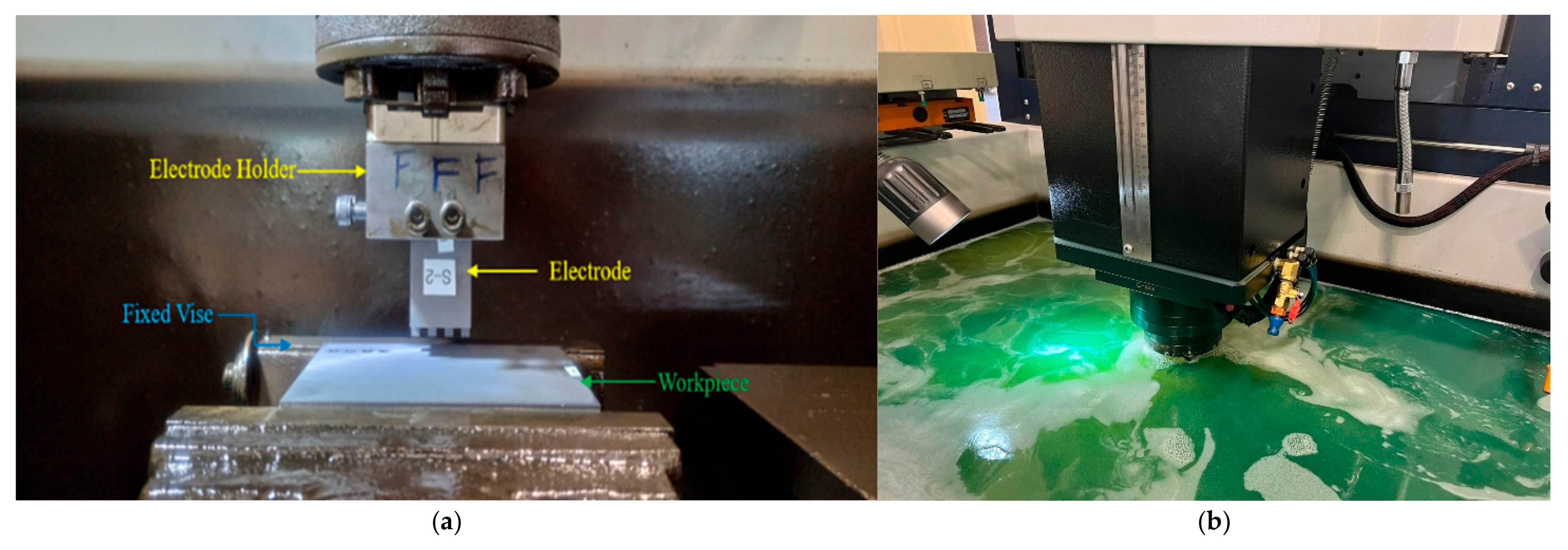
2.1. Experimental Setup
2.2. Methodology
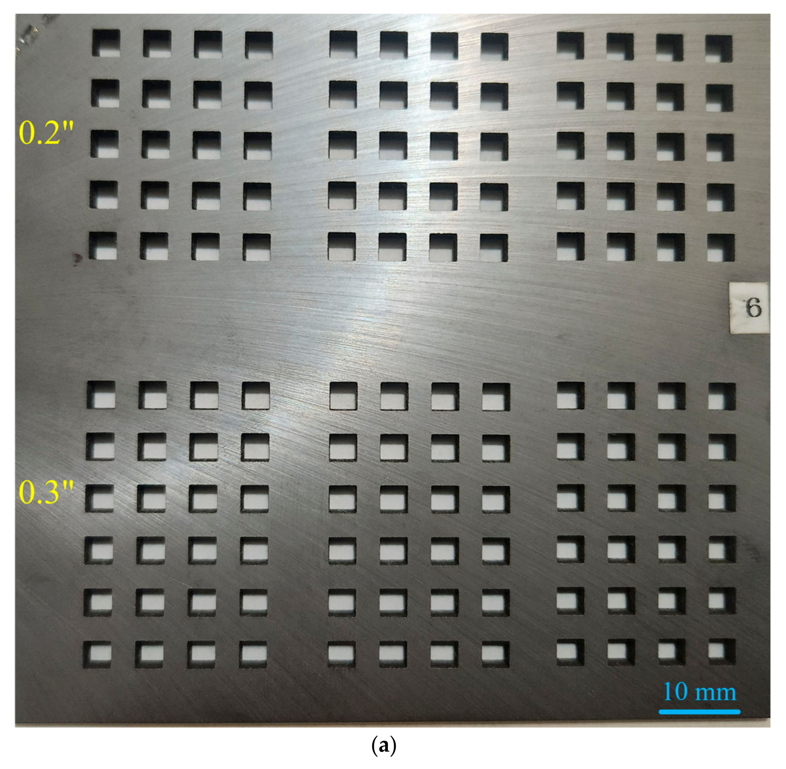
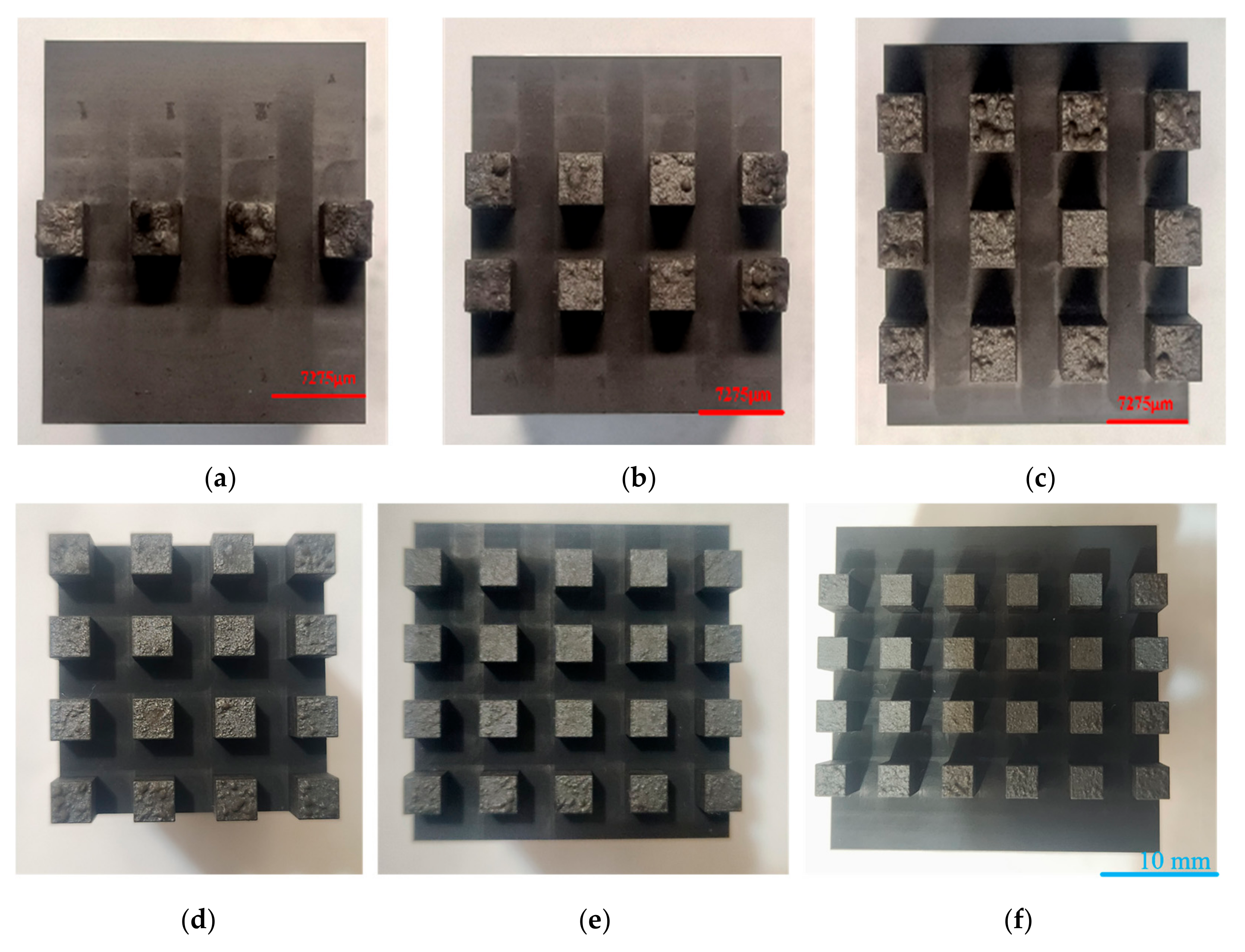
2.2.1. Electrode Fabrication
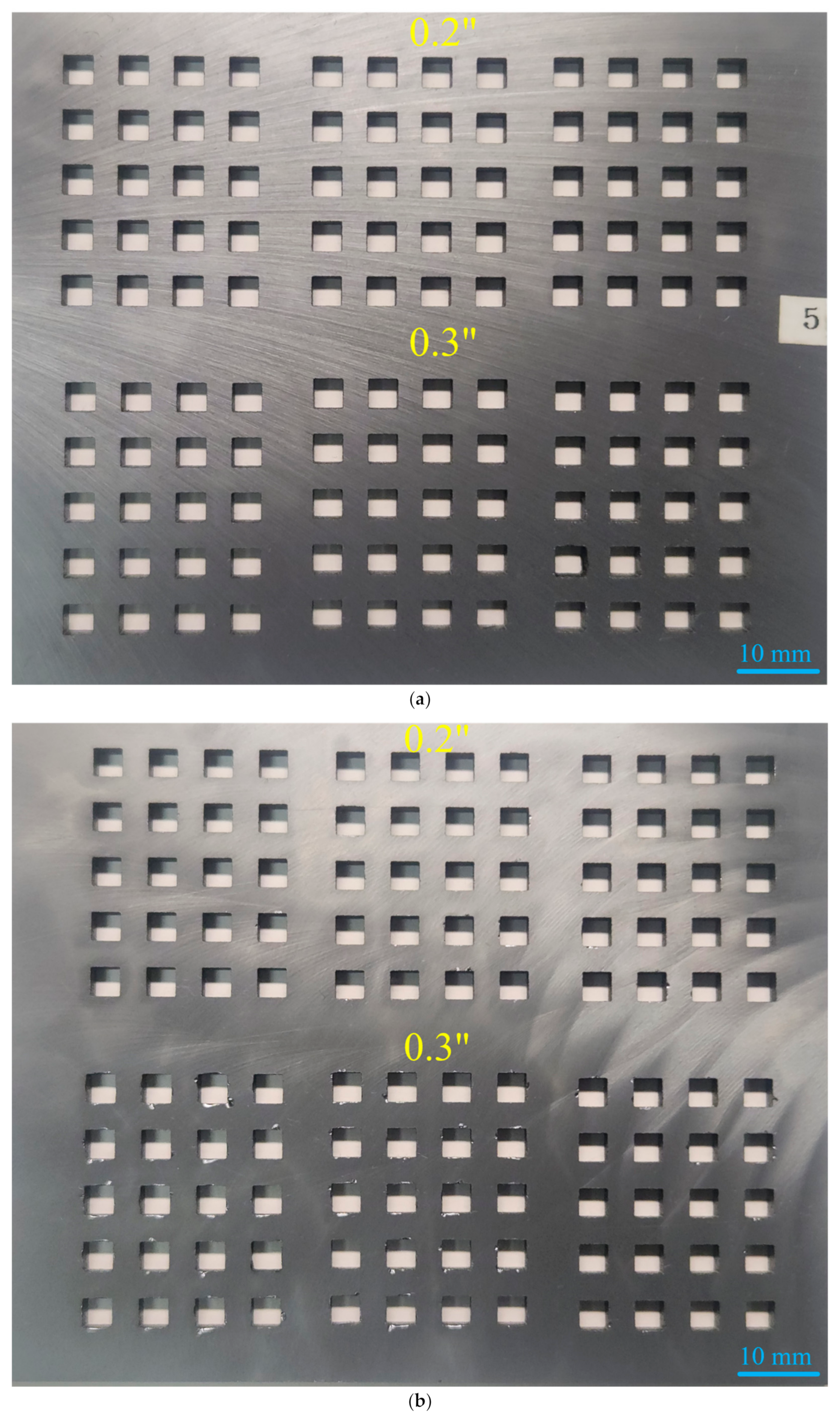
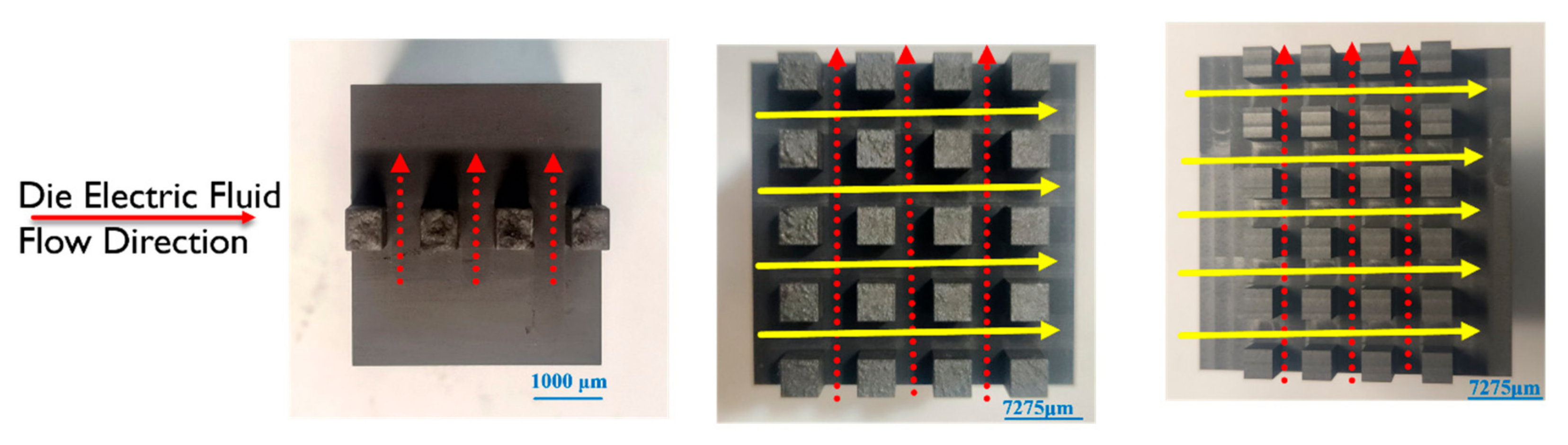
Varying Arrays of Electrode Legs
Varying Depth of Electrode Legs
Varying Thickness of Hollow Electrodes
2.2.2. Machining Parameters for EDM of Silicon
2.3. Characterization of Tool Electrodes and Silicon Workpieces
3. Results and Discussion
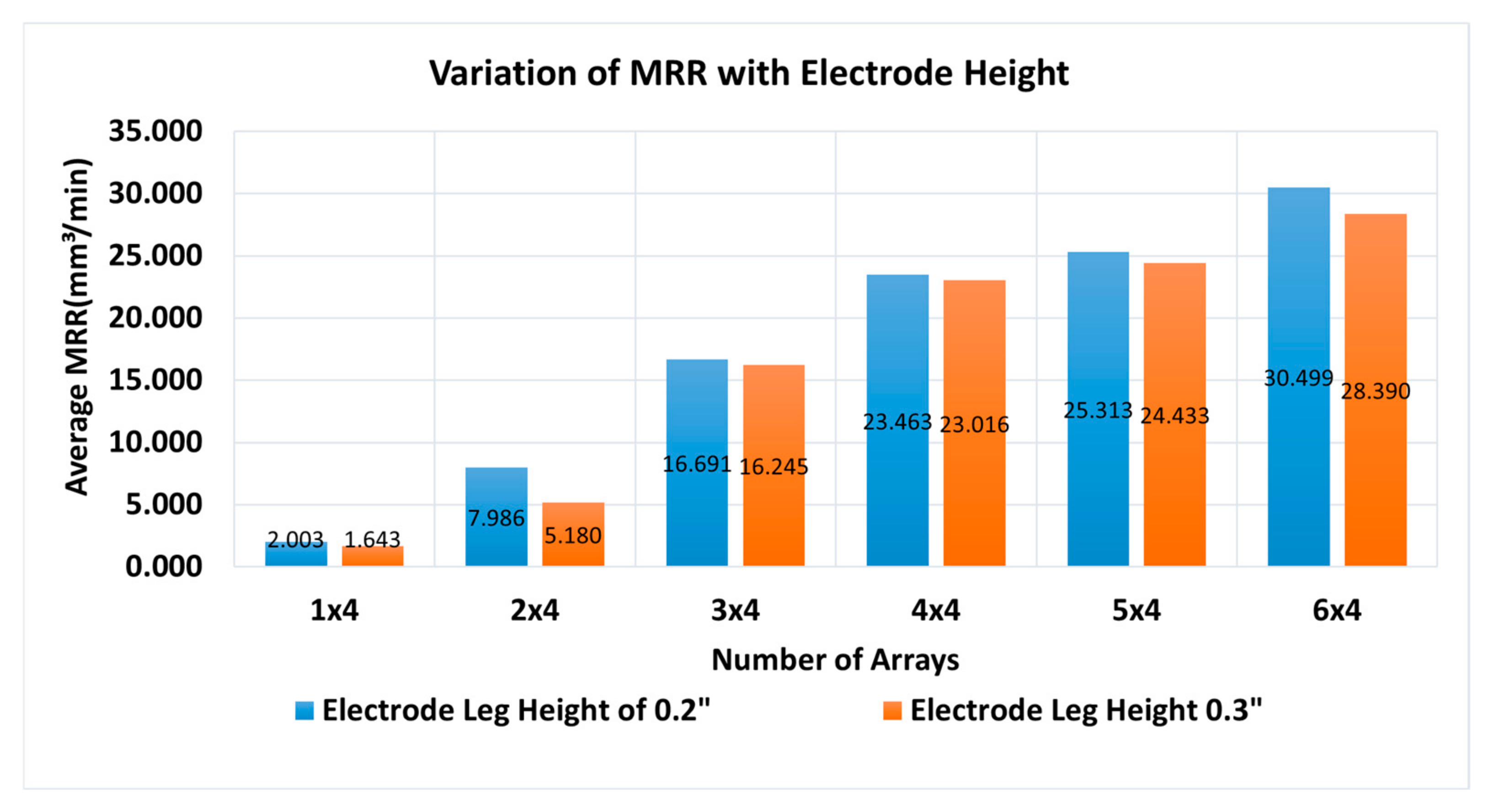
3.1. Effect of Electrode Arrays on Machining Speed with Varied Electrode Leg Heights
3.1.1. Fabrication of Electrodes, Measurements, and Analysis
3.1.2. Analysis of Machining Time and Material Removal Rate (MRR)
3.1.3. Analysis of Quality of the Machined Features on Silicon
3.1.4. Analysis of Tool Wear Ratio
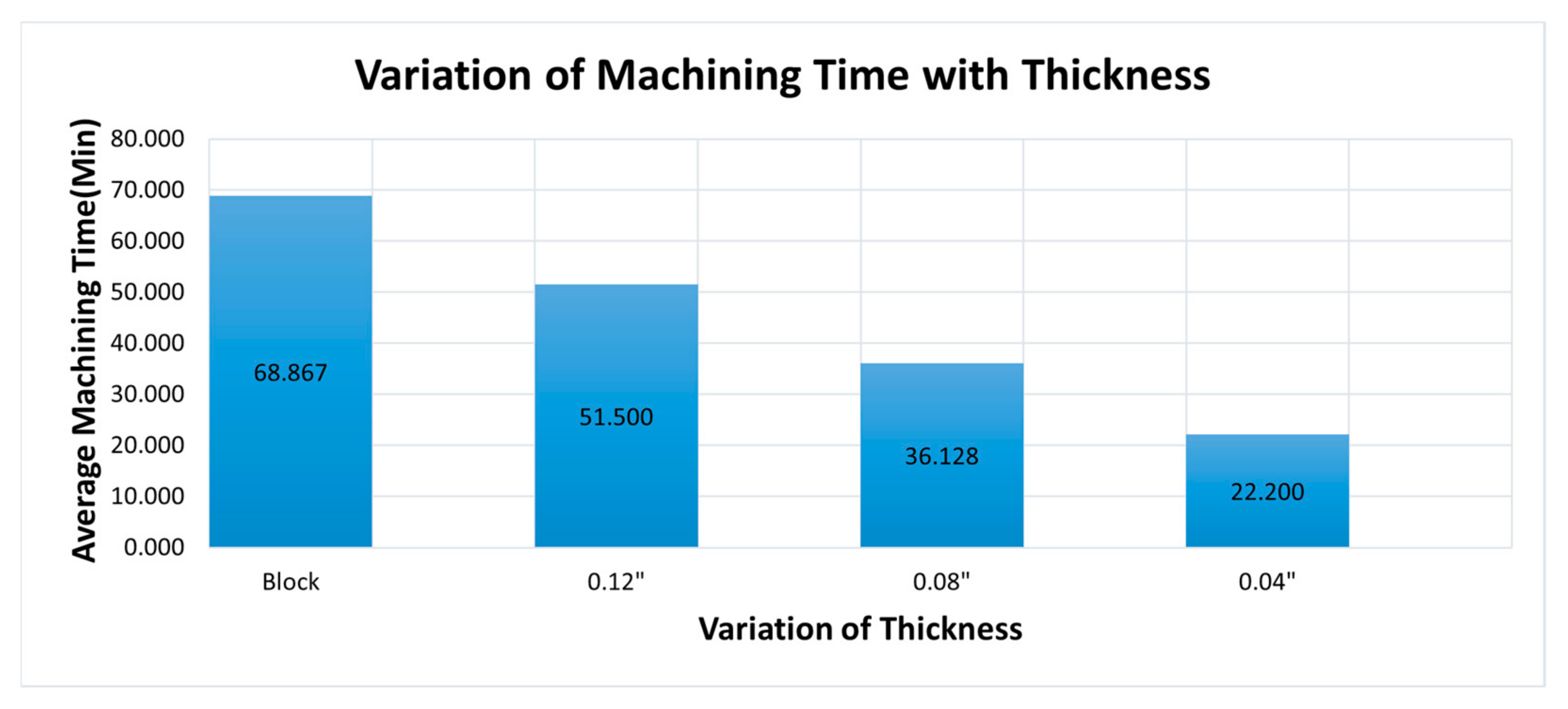
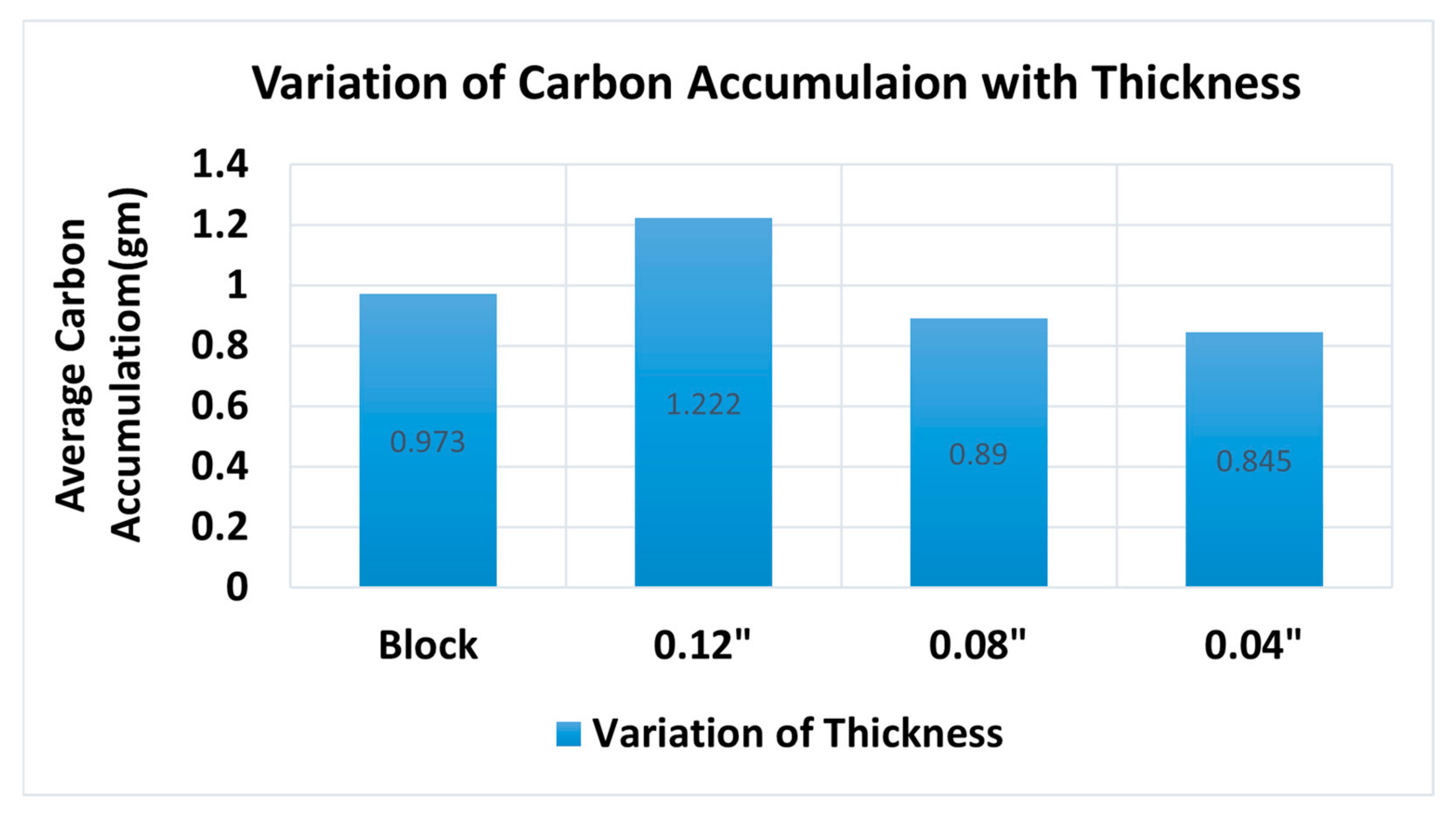
3.2. Effects of Hollow Electrodes on Machining Speed with Varied Wall Thickness
3.2.1. Fabrication of Electrodes, Measurements, and Analysis
3.2.2. Analysis of Machining Time and Material Removal Rate
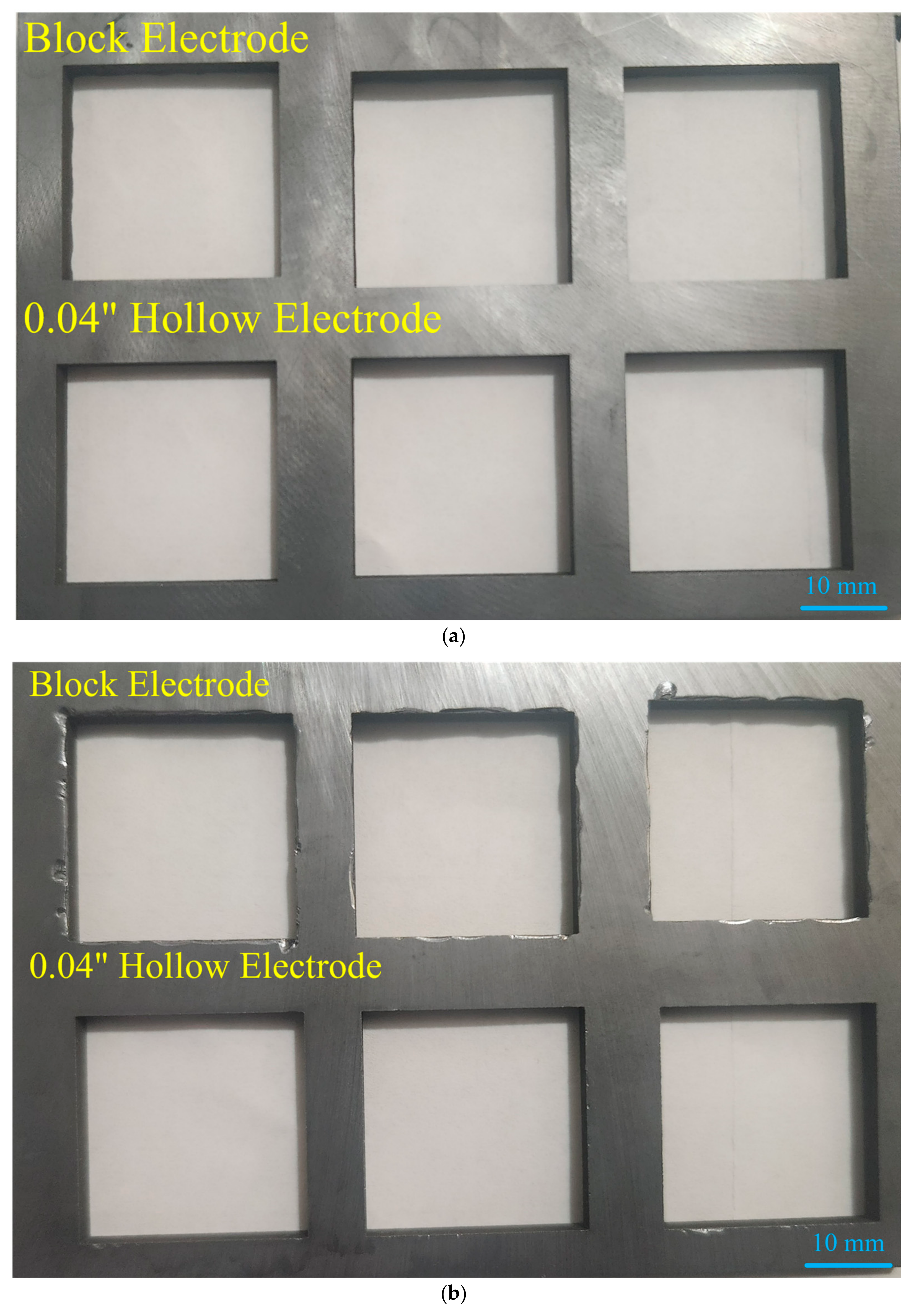
3.2.3. Analysis of the Quality of Machined Features on Silicon
3.2.4. Analysis of Tool Wear Ratio
4. Conclusions
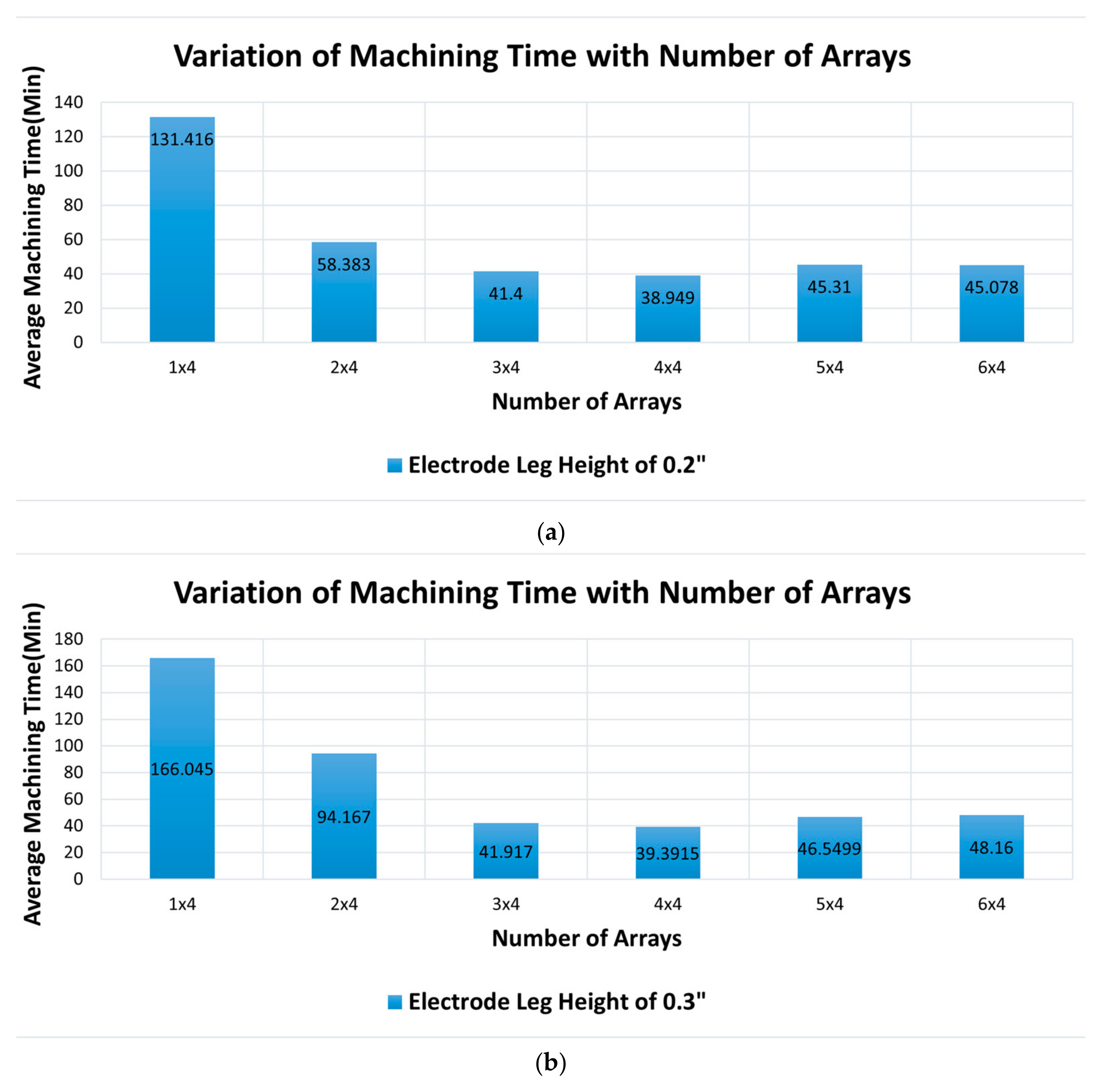
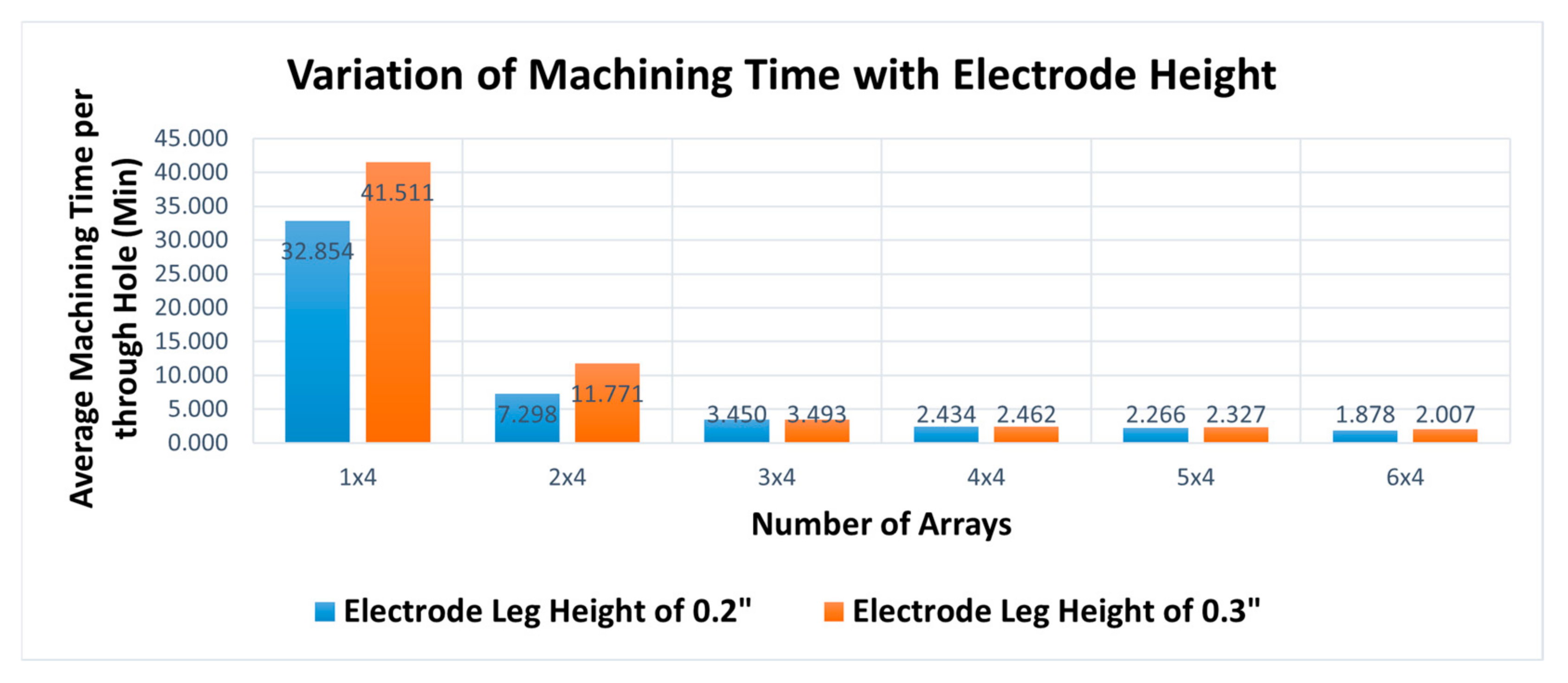
- The increased arrays of electrode legs have a positive effect on the machining time and material removal rate. With the increment in arrays of the electrode, the machining time required for each slot decreased and the material removal rate per slot increased, irrespective of the height of the electrode leg. For both cases of electrode leg heights (0.2″ and 0.3″), 6 × 4 arrays of electrodes required less time per slot and provided a higher material removal rate than the 5 × 4, 4 × 4, 3 × 4, 2 × 4, and 1 × 4 arrays of electrodes;
- For 1 × 4 and 2 × 4 arrays of electrodes, smaller electrode leg heights performed better in terms of the MRR or machining time. For the case of higher arrays of electrodes (3 × 4, 4 × 4, 5 × 4, and 6 × 4) there are no significant differences in the MRR for different electrode leg heights. It is found that with increased arrays of electrodes, the effect of the electrode’s leg height became insignificant;
- The overall quality of the machined features on the silicon workpiece became better with an increased array of electrodes due to improvements in the flushing conditions. The mirror image of the graphite electrode on the silicon workpiece for 6 × 4 arrays of electrodes is closer to the desired output than those of 5 × 4, 4 × 4, 3 × 4, 2 × 4, and 1 × 4 arrays of electrodes. For both heights, the overall quality of the features of the mirror image of the graphite electrode leg on the workpiece is nearly comparable;
- For both cases of electrode leg heights, carbon deposition per electrode has gradually decreased as the arrays of electrodes have increased. Carbon deposition per electrode leg is quite similar for different arrays of electrodes for both electrode heights. Carbon deposition also plays a critical role in determining the material removal rate and edge quality of the machined features. The higher the accumulation of carbon, the higher the chance of secondary sparking, thus resulting in chipping and zagged edges of machined features on silicon;
- Careful electrode array design, considering the flow direction of dielectric fluid and selecting an ideal number of channels in between electrode arrays and leg heights of the electrodes, can increase both the machining speed (i.e., productivity) and feature quality (i.e., dimensional accuracy, quality of the machined parts, and edge surface finish) of the machined features on silicon via die-sinking EDM;
- The hollow electrodes can provide a faster machining speed compared to fully solid block electrodes when machining the same through features on silicon. With the decrement in the wall thickness of the hollow electrode, there is an increase in the value of the MRR and a reduction in the required machining time to complete a slot. In terms of the MRR, the block electrode ranks the lowest when compared to the hollow electrodes with varied wall thicknesses;
- The overall quality of the machined features on the silicon workpiece became better with a decreased thickness of the electrode due to the smaller sparking area resulting in higher energy density. The mirror image of the graphite electrode on the silicon workpiece for the 0.04″-thick electrode (quality of square through holes on silicon) is better than those of the hollow electrodes with 0.08″ and 0.12″ thicknesses and the block electrode. In terms of the quality of the parts, the block electrode ranks the lowest, providing a zagged edge surface finish at the exit of machined square holes, and the 0.04″-thick hollow electrode ranks at the top, providing clear edges with minimum variations. The improved quality of the machined features using hollow electrodes is associated with less carbon deposition on the thinner walls of hollow electrodes, thus minimizing the chances of secondary sparking, i.e., arcing and short-circuiting.
5. Future Research
- The study found that 6 × 4 arrays and the 0.04″-thick wall showed the optimum results in terms of the MRR and surface quality of machined features in Silicon, which comes with some potential trade-offs. One of the major trade-offs is the higher fabrication time due to the intricate design of electrodes with 6 × 4 arrays and a 0.04″ thickness for mass production/industrial adoption, which can be easily eliminated by using high-end CNC milling;
- Furthermore, a high-flow-rate-capacity peristaltic pump can be attached to the hollow square electrode for pressure flushing to improve the flushing conditions and reduce the machining time. Vibration on the workpiece can also be used for better flushing to improve the MRR for slotting silicon in die-sinking EDM;
- From the literature review, it can be found that powder-mixed EDM generated the least surface roughness on the machined parts. So, powder-mixed EDM can be used to improve the surface finish in the future, as in the present experiments, we have seen chipping along the edge of the machined holes, especially at the exit side;
- It has been found that gluing conductive material to silicon improves the machining performance, including the surface finish, through more uniform and stable discharge, which can also be used in the future studies;
- Future studies should also focus on applying vibroacoustic diagnostics to understand whether dielectric fluid effectively removes the sludge/debris or not. By analyzing the amplitude of the vibroacoustic signals, information regarding the change in the concentration of debris at the machined zone can be identified, thus indicating the efficacy of the flushing mechanism.
Author Contributions
Funding
Institutional Review Board Statement
Informed Consent Statement
Data Availability Statement
Acknowledgments
Conflicts of Interest
Appendix A

| Case-1 (Intended Electrode Leg Height is 0.2″ = 5080 μm) | ||||||
|---|---|---|---|---|---|---|
| Number of Arrays | Sample | Leg Length (μm) | Leg Width (μm) | Leg Height (μm) | Length Amid Legs (μm) | Width Amid Legs (μm) |
| 1 × 4 (Row × Column) | Sample-1 | 3620.94 | 3627.12 | 5082.35 | 3620.69 | - |
| Sample-2 | 3615.54 | 3631.29 | 5058.82 | 3628.02 | - | |
| Sample-3 | 3611.45 | 3623.38 | 5094.12 | 3628.02 | - | |
| 2 × 4 (Rows × Column) | Sample-1 | 3615.19 | 3644.08 | 5070.58 | 3627.13 | 3606.01 |
| Sample-2 | 3642.29 | 3613.25 | 5062.87 | 3610.35 | 3631.65 | |
| Sample-3 | 3628.18 | 3614.26 | 5072.15 | 3619.15 | 3621.95 | |
| 3 × 4 (Row × Column) | Sample-1 | 3632.31 | 3614.86 | 5095.38 | 3607.91 | 3615.18 |
| Sample-2 | 3634.92 | 3625.58 | 5085.02 | 3611.24 | 3625.27 | |
| Sample-3 | 3614.10 | 3630.18 | 5069.86 | 3625.35 | 3614.75 | |
| 4 × 4 (Row × Column) | Sample-1 | 3634.34 | 3615.87 | 5076.62 | 3637.20 | 3623.07 |
| Sample-2 | 3643.89 | 3608.79 | 5070.25 | 3629.68 | 3637.49 | |
| Sample-3 | 3635.58 | 3621.96 | 5082.68 | 3630.88 | 3630.57 | |
| 5 × 4 (Row × Column) | Sample-1 | 3651.33 | 3615.25 | 5065.45 | 3627.32 | 3619.25 |
| Sample-2 | 3660.39 | 3614.68 | 5071.01 | 3633.31 | 3626.16 | |
| Sample-3 | 3663.03 | 3620.53 | 5063.13 | 3621.87 | 3630.28 | |
| 6 × 4 (Row × Column) | Sample-1 | 3644.85 | 3625.16 | 5059.87 | 3620.35 | 3607.91 |
| Sample-2 | 3635.58 | 3620.53 | 5076.26 | 3619.15 | 3611.24 | |
| Sample-3 | 3626.43 | 3608.13 | 5070.25 | 3607.91 | 3625.35 | |
| Case-2 (Intended Electrode Leg Height is 0.3″ = 7620 μm) | ||||||
| 1 × 4 (Row × Column) | Sample-1 | 3597.76 | 3566.58 | 7714.29 | 3641.47 | - |
| Sample-2 | 3619.24 | 3598.64 | 7733.33 | 3631.69 | - | |
| Sample-3 | 3585.15 | 3619.34 | 7704.76 | 3643.70 | - | |
| 2 × 4 (Row × Column) | Sample-1 | 3595.47 | 3604.18 | 7742.86 | 3639.03 | 3639.39 |
| Sample-2 | 3618.25 | 3626.59 | 7701.15 | 3625.18 | 3614.18 | |
| Sample-3 | 3605.92 | 3615.21 | 7695.24 | 3631.84 | 3621.17 | |
| 3 × 4 (Row × Column) | Sample-1 | 3619.16 | 3602.66 | 7712.38 | 3619.63 | 3631.59 |
| Sample-2 | 3625.72 | 3615.91 | 7730.56 | 3607.92 | 3626.62 | |
| Sample-3 | 3632.29 | 3642.27 | 7733.33 | 3604.75 | 3601.58 | |
| 4 × 4 (Row × Column) | Sample-1 | 3652.33 | 3616.23 | 7729.35 | 3629.27 | 3630.57 |
| Sample-2 | 3659.72 | 3624.80 | 7737.89 | 3643.89 | 3619.25 | |
| Sample-3 | 3661.03 | 3621.43 | 7740.56 | 3635.58 | 3626.16 | |
| 5 × 4 (Row × Column) | Sample-1 | 3645.96 | 3660.88 | 7719.25 | 3625.35 | 3625.35 |
| Sample-2 | 3656.63 | 3657.32 | 7722.88 | 3637.20 | 3637.20 | |
| Sample-3 | 3648.16 | 3663.66 | 7720.75 | 3629.68 | 3629.68 | |
| 6 × 4 (Row × Column) | Sample-1 | 3639.29 | 3640.35 | 7735.75 | 3630.57 | 3566.58 |
| Sample-2 | 3645.89 | 3625.26 | 7740.02 | 3619.25 | 3598.64 | |
| Sample-3 | 3635.58 | 3641.43 | 7727.63 | 3626.16 | 3619.34 | |
| Type of Electrode | Electrode | Workpiece (Entry) | Workpiece (Exit) | |||
|---|---|---|---|---|---|---|
| Average Length (μm) | Average Width (μm) | Average Length (μm) | Average Width (μm) | Average Length (μm) | Average Width (μm) | |
| Block | 25,463.5 | 25,467.73 | 26,289.42 | 26,326.31 | 26,620.65 | 26,656.71 |
| 0.12″ | 25,467.73 | 25,471.97 | 26,253.40 | 26,326.49 | 26,362.77 | 26,399.44 |
| 0.08″ | 25,471.97 | 25,467.73 | 26,326.49 | 26,252.98 | 26,362.98 | 26,253.16 |
| 0.04″ | 25,467.73 | 25,741.97 | 26,255.85 | 26,252.98 | 26,179.44 | 26,179.83 |
Appendix B


References
- Jia, Z.; Li, S.; Ma, G.; Shao, W.; Liu, F.; Qiao, C. Modeling and control of electrical discharge wire sawing of single-crystal silicon. J. Manuf. Process. 2024, 117, 289–301. [Google Scholar] [CrossRef]
- Deka, S.; Kar, S.; Patowari, P.K. Machinability of Silicon and German Silver in Micro Electrical Discharge Machining: A Comparative Study. Silicon 2021, 13, 1065–1077. [Google Scholar] [CrossRef]
- Zhang, Y.; Zhang, Z.; Zhang, Y.; Liu, D.; Wu, J.; Huang, Y.; Zhang, G. Study on machining characteristics of magnetically controlled laser-induced plasma micro-machining single-crystal silicon. J. Adv. Res. 2021, 30, 39–51. [Google Scholar] [CrossRef] [PubMed]
- Verma, A.S.; Singh, S. Parametric optimization of silicon slicing using wire electro discharge machining. Mater. Today Proc. 2020, 44, 4293–4298. [Google Scholar] [CrossRef]
- Zhu, X.; Li, G.; Mo, J.; Ding, S. Electrical discharge machining of semiconductor materials: A review. J. Mater. Res. Technol. 2023, 25, 4354–4379. [Google Scholar] [CrossRef]
- Peng, W.Y.; Liao, Y.S. Study of electrical discharge machining technology for slicing silicon ingots. J. Mater. Process. Technol. 2003, 140, 274–279. [Google Scholar] [CrossRef]
- Singh, R.; Kumar, A. Analysis of Wire EDM machining parameters on machining of Silicon material. Int. J. Mech. Ind. Technol. 2021, 8, 35–43. [Google Scholar]
- Joshi, K.; Ananya, A.; Bhandarkar, U.; Joshi, S.S. Ultra-thin silicon wafer slicing using wire-EDM for solar cell application. Mater. Des. 2017, 124, 158–170. [Google Scholar] [CrossRef]
- Fonda, P.; Chan, M.L.; Heidari, A.; Nakamoto, K.; Sano, S.; Horsley, D.D.; Yamazaki, K. The application of diamond-based electrodes for efficient EDMing of silicon wafers for freeform MEMS device fabrication. Procedia CIRP 2013, 6, 280–285. [Google Scholar] [CrossRef]
- Murray, J.W.; Fay, M.W.; Kunieda, M.; Clare, A.T. TEM study on the electrical discharge machined surface of single-crystal silicon. J. Mater. Process. Technol. 2013, 213, 801–809. [Google Scholar] [CrossRef]
- Ganapathy, S.; Palanivendhan, M.; Balasubramanian, P.; Susitra, K. Process parameter of EDM to optimize material Removal Rate using Box Behnken’s design. Mater. Today Proc. 2022, 82, 38–42. [Google Scholar] [CrossRef]
- Świercz, R.; Oniszczuk-Świercz, D.; Chmielewski, T. Multi-response optimization of electrical discharge machining using the desirability function. Micromachines 2019, 10, 72. [Google Scholar] [CrossRef] [PubMed]
- Verma, A.S.; Singh, S. Investigation and multi-objective optimization of monocrystalline silicon wafering using wire electro-discharge machining. Proc. Inst. Mech. Eng. Part C J. Mech. Eng. Sci. 2022, 236, 7221–7235. [Google Scholar] [CrossRef]
- Dongre, G.; Zaware, S.; Dabade, U.; Joshi, S.S. Multi-objective optimization for silicon wafer slicing using wire-EDM process. Mater. Sci. Semicond. Process. 2015, 39, 793–806. [Google Scholar] [CrossRef]
- Maccarini, G.; Pellegrini, G.; Ravasio, C. Effects of the properties of workpiece, electrode and dielectric fluid in micro-EDM drilling process. Procedia Manuf. 2020, 51, 834–841. [Google Scholar] [CrossRef]
- Bhaumik, M.; Maity, K. Effect of different tool materials during EDM performance of titanium grade 6 alloy. Eng. Sci. Technol. Int. J. 2018, 21, 507–516. [Google Scholar] [CrossRef]
- Rahul; Mishra, D.K.; Datta, S.; Masanta, M. Effects of Tool Electrode on EDM Performance of Ti-6Al-4V. Silicon 2018, 10, 2263–2277. [Google Scholar] [CrossRef]
- Elumalai, B.; Gowri, S.; Hariharan, P.; Pillai, K.V.A. Experimental investigations on μeD milling of inconel 718 with nano SiC abrasive mixed dielectric. Mater. Res. 2022, 25, e20210468. [Google Scholar] [CrossRef]
- Murugesh, S.; Manikandan, N.; Subramaniyan, M.; Chockalingam, S.; Surendar, G. Experimental investigation of electrode shape configuration in sustainable electric discharge machining process. IOP Conf. Ser. Mater. Sci. Eng. 2021, 1057, 012068. [Google Scholar] [CrossRef]
- Liu, C.; Rashid, A.; Jahan, M.P.; Ma, J. Machining of High Aspect Ratio Micro-Holes on Titanium Alloy Using Silver Nano Powder Mixed Micro EDM Drilling. In ASME International Mechanical Engineering Congress and Exposition; American Society of Mechanical Engineers: New York, NY, USA, 2020; Volume 59377, p. V02AT02A011. [Google Scholar]
- Niamat, M.; Sarfraz, S.; Aziz, H.; Jahanzaib, M.; Shehab, E.; Ahmad, W.; Hussain, S. Effect of Different Dielectrics on Material Removal Rate, Electrode Wear Rate and Microstructures in EDM. Procedia CIRP 2017, 60, 2–7. [Google Scholar] [CrossRef]
- Goiogana, M.; Elkaseer, A. Self-flushing in EDM drilling of Ti6Al4V using rotating shaped electrodes. Materials 2019, 12, 989. [Google Scholar] [CrossRef] [PubMed]
- Kachhap, S.; Singh, A.; Kumar, S. Performance evaluation of different electrode geometries in electric discharge drilling of MMCs. Int. J. Mech. Eng. Robot. Res. 2019, 8, 531–535. [Google Scholar] [CrossRef]
- Abbas, A.A.; Aabid, M. Effect of Current and Pulse on Time on MRR and EWR for different inner electrode shape of EDM process. Glob. J. Eng. Sci. Res. Manag. 2018, 5, 13–26. [Google Scholar] [CrossRef]
- Lin, Z.; Guo, Z.; Jiang, S.; Liu, G.; Liu, J. Electrical discharge drilling of metal matrix composites with a hollow hexagonal electrode. Adv. Compos. Lett. 2018, 27, 193–203. [Google Scholar] [CrossRef]
- Khosrozadeh, B.; Shabgard, M. Effects of hybrid electrical discharge machining processes on surface integrity and residual stresses of Ti-6Al-4V titanium alloy. Int. J. Adv. Manuf. Technol. 2017, 93, 1999–2011. [Google Scholar] [CrossRef]
- Munz, M.; Risto, M.; Haas, R. Specifics of flushing in electrical discharge drilling. Procedia CIRP 2013, 6, 83–88. [Google Scholar] [CrossRef]
- Chuvaree, S.; Kanlayasiri, K. Effects of side flushing and multi-aperture inner flushing on characteristics of electrical discharge machining macro deep holes. Metals 2021, 11, 148. [Google Scholar] [CrossRef]
- Uhlmann, E.; Domingos, D.C. Investigations on Vibration-assisted EDM-machining of Seal Slots in High-Temperature Resistant Materials for Turbine Components—Part II. Procedia CIRP 2016, 42, 334–339. [Google Scholar] [CrossRef]
- Amorim, F.L.; Weingaertner, W.L. The behavior of graphite and copper electrodes on the finish die-sinking electrical discharge machining (EDM) of AISI P20 tool steel. J. Braz. Soc. Mech. Sci. Eng. 2007, 29, 366–371. [Google Scholar] [CrossRef]
- Okamoto, Y.; Ikeda, T.; Kurihara, H.; Okada, A.; Kido, M. Control of Kerf Width in Multi-wire EDM Slicing of Semiconductors with Circular Section. Procedia CIRP 2018, 68, 100–103. [Google Scholar] [CrossRef]
- Kane, M.M.; Kulkarni, S.V.; Bahirat, H.J.; Joshi, S.S. Analysis of Electrical Forces in Multi-wire EDM for Semiconductors. Procedia CIRP 2020, 95, 302–307. [Google Scholar] [CrossRef]
- Kunieda, M.; Ojima, S. Improvement of EDM efficiency of silicon single crystal through ohmic contact. Precis. Eng. 2000, 24, 185–190. [Google Scholar] [CrossRef]
- Available online: https://poco.entegris.com/en/home/products/premium-graphite/edm-grades/edm-3.html (accessed on 3 June 2025).
- Square End Mill. Available online: https://www.mscdirect.com/product/details/00037689 (accessed on 3 June 2025).
- Jahan, M.P. Electrical Discharge Machining (EDM) Types, Technologies and Applications; Nova Science Publishers, Inc.: Hauppauge, NY, USA, 2015. [Google Scholar]
- Available online: https://sodick.eu/about-sodick/sodicks-technology/edm-technology (accessed on 3 June 2025).
- Marafona, J. Black layer characterisation and electrode wear ratio in electrical discharge machining (EDM). J. Mater. Process. Technol. 2007, 184, 27–31. [Google Scholar] [CrossRef]
- Zan, S.; Wang, Z.; Jia, Y.; Chi, G.; Wang, Y. Study of graphite tool wear in EDM with water-based dielectrics and EDM oil. Procedia CIRP 2020, 95, 414–418. [Google Scholar] [CrossRef]
- Jahan, M.P.; Rahman, M.; Wong, Y.S. Study of the diffusion of carbon, its sources, and effect on finishing micro-EDM performance of cemented carbide. J. Mater. Eng. Perform. 2012, 21, 1655–1668. [Google Scholar] [CrossRef]
- Klocke, F.; Schwade, M.; Klink, A.; Veselovac, D. Analysis of material removal rate and electrode wear in sinking EDM roughing strategies using different graphite grades. Procedia CIRP 2013, 6, 163–167. [Google Scholar] [CrossRef]
- Rashid, A.; Perveen, A.; Jahan, M.P. Understanding novel assisted electrode from a theoretical and experimental perspectives for EDM of aluminum nitride ceramics. Int. J. Adv. Manuf. Technol. 2021, 116, 2959–2973. [Google Scholar] [CrossRef]
- Jahan, M.P.; Lieh, T.W.; Wong, Y.S.; Rahman, M. An experimental investigation into the electro-discharge machining behavior of p-type silicon. Int. J. Adv. Manuf. Technol. 2011, 57, 617–637. [Google Scholar] [CrossRef]
- Ashtiani, H.R.R.; Hojati, F. The influences of spark energy density on the electrical discharge machining (EDM). Adv. Mater. Process. Technol. 2021, 8, 3165–3181. [Google Scholar] [CrossRef]
- Dwaraka, R.; Arunachalam, N. Investigation on non-invasive process monitoring of Die Sinking EDM using Acoustic Emission signals. Procedia Manuf. 2018, 26, 1471–1482. [Google Scholar] [CrossRef]
- Liu, C.; Duong, N.; Jahan, M.P.; Ma, J.; Kirwin, R. Experimental investigation and numerical simulation of micro-EDM of bulk metallic glass with focus on crater sizes. Procedia Manuf. 2019, 34, 275–286. [Google Scholar] [CrossRef]
- Jahan, M.P.; Wong, Y.S.; Rahman, M. A Comparative Study of Transistor and RC Pulse Generators for Micro-EDM of Tungsten Carbide. Int. J. Precis. Eng. Manuf. 2008, 9, 3–10. [Google Scholar]


| Description | Data |
|---|---|
| Workpiece material | Silicon |
| Workpiece length | ~110 mm |
| Workpiece width | ~80 mm |
| Workpiece thickness | ~3.74 mm |
| Density | 2.33 gm/cm3 |
| Resistivity | 0.0–0.05 Ωcm |
| Melting point | 1414 °C |
| Boiling point | 3265 °C |
| Description | Data |
|---|---|
| Electrode material | Graphite |
| Grade | Poco-3 |
| Average particle size | <5 µm |
| Flexural strength | 13,300 psi (935 kg/cm2) |
| Compressive strength | 18,100 psi (1273 kg/cm2) |
| Hardness | 73 shore |
| Electrical resistivity | 615 µΩ-in |
| Melting point | 3650 °C |
| Criteria | Description |
|---|---|
| X-Axis travel | 400 mm |
| Y-Axis travel | 300 mm |
| Z-Axis travel | 350 mm |
| Maximum workpiece weight | 1200 kg |
| Maximum electrode weight | 60 kg |
| C codes | 2000 sets |
| Peak current | 0–288 amps |
| Pulse on time | 0–2000 µs |
| Pulse off time | 0–4000 µs |
| Discharge voltage | 140 V–235 V DC |
| Discharge time | 0.1 s–99.9 s |
| Gap voltage | 20–120 V |
| Swing radius | 0–999.99 mm |
| Electrode polarity | Reversible |
| Discharge server speed | Controllable (1 to 100%) |
| Slag removing speed | Controllable (1 to 100%) |
| Optimization Level | Peak Current (A) | Pulse on Time (μs) | Pulse off Time (μs) | Discharge Time (s) | Machining Time (min) | Depth of Machining (in) |
|---|---|---|---|---|---|---|
| Level 1 | 4 | 100 | 50 | 0.8 | 49.5 | 0.128 |
| Level 2 | 6 | 150 | 75 | 0.8 | 49.5 | 0.0672 |
| Level 3 | 8 | 200 | 100 | 0.8 | 49.5 | 0.0227 |
| Criteria | Description |
|---|---|
| C code | 408 |
| Peak current | 4 A |
| Pulse on time | 100 µs |
| Pulse off time | 50 µs |
| Discharge voltage | 235 V (DC) |
| Discharge time | 0.8 s |
| Discharge height | 0.039″ |
| Slag removing speed | 60% |
| Discharge server speed | 70% |
| Gap voltage | 50 |
| Swing radius | 0 |
| Electrode polarity | Positive |
| Number of Electrode Legs | Marking of Legs | Electrode | Workpiece (Entry) | Workpiece (Exit) | |||
|---|---|---|---|---|---|---|---|
| Length (μm) | Width (μm) | Length (μm) | Width (μm) | Length (μm) | Width (μm) | ||
| 4 (1 × 4) | Leg-1 | 3639.03 | 3618.86 | 4162.74 | 4092.19 | 3739.43 | 3965.19 |
| Leg-2 | 3628.03 | 3622.55 | 4280.34 | 4120.41 | 3777.05 | 3781.75 | |
| Leg-3 | 3625.36 | 3635.36 | 4068.67 | 4162.75 | 3838.19 | 3805.27 | |
| Leg-4 | 3591.34 | 3631.70 | 4040.45 | 4106.30 | 3800.56 | 4007.53 | |
| 8 (2 × 4) | Leg-1 | 3639.03 | 3624.36 | 3974.60 | 3969.90 | 3908.75 | 3894.64 |
| Leg-2 | 3609.69 | 3620.69 | 3998.12 | 3951.08 | 3951.08 | 4125.12 | |
| Leg-3 | 3617.02 | 3672.05 | 4016.93 | 3965.19 | 4021.64 | 3993.42 | |
| Leg-4 | 3606.02 | 3672.05 | 4054.56 | 3984.01 | 3777.05 | 3805.27 | |
| Leg-5 | 3650.04 | 3613.35 | 3974.60 | 3998.12 | 3974.60 | 3852.31 | |
| Leg-6 | 3606.02 | 3609.69 | 3951.08 | 4016.93 | 3941.68 | 3988.71 | |
| Leg-7 | 3609.69 | 3675.72 | 4021.64 | 4040.45 | 4101.60 | 4134.55 | |
| Leg-8 | 3584.01 | 3664.73 | 3965.19 | 4054.56 | 3767.64 | 3814.69 | |
| 12 (3 × 4) | Leg-1 | 3609.69 | 3635.37 | 3913.45 | 4002.83 | 3781.75 | 3932.27 |
| Leg-2 | 3613.35 | 3639.03 | 4007.53 | 3974.60 | 3814.68 | 3777.06 | |
| Leg-3 | 3620.69 | 3628.03 | 3988.71 | 3998.12 | 3852.31 | 3786.46 | |
| Leg-4 | 3653.71 | 3617.03 | 3984.01 | 3955.80 | 3998.12 | 4139.24 | |
| Leg-5 | 3617.02 | 3609.69 | 3899.34 | 3993.42 | 3786.45 | 3777.05 | |
| Leg-6 | 3639.03 | 3609.69 | 3988.71 | 3993.42 | 3819.38 | 3781.75 | |
| Leg-7 | 3613.36 | 3606.02 | 3998.12 | 3998.13 | 3791.16 | 3795.86 | |
| Leg-8 | 3661.04 | 3606.02 | 3979.30 | 3979.30 | 3842.90 | 3800.56 | |
| Leg-9 | 3620.69 | 3617.03 | 3959.51 | 3997.18 | 3871.12 | 3828.79 | |
| Leg-10 | 3646.38 | 3613.35 | 4002.82 | 4002.82 | 3828.79 | 3814.68 | |
| Leg-11 | 3635.38 | 3598.70 | 3988.71 | 3936.97 | 3805.27 | 3758.23 | |
| Leg-12 | 3657.38 | 3598.69 | 3998.12 | 3918.16 | 3819.38 | 3805.27 | |
| 16 (4 × 4) | Leg (Average) | 3637.94 | 3615.54 | 3945.25 | 3911.92 | 3834.66 | 3828.55 |
| 20 (5 × 4) | Leg (Average) | 3658.25 | 3616.62 | 3969.73 | 3914.67 | 3828.06 | 3780.69 |
| 24 (6 × 4) | Leg (Average) | 3635.62 | 3617.94 | 3923.05 | 3856.27 | 3781.76 | 3799.85 |
| Number of Electrode Legs | Marking of Leg | Electrode | Workpiece (Entry) | Workpiece (Exit) | |||
|---|---|---|---|---|---|---|---|
| Length (μm) | Width (μm) | Length (μm) | Width (μm) | Length (μm) | Width (μm) | ||
| 4 (1 × 4) | Leg-1 | 3576.67 | 3580.34 | 3951.09 | 4176.86 | 3786.45 | 3781.75 |
| Leg-2 | 3602.35 | 3580.34 | 4087.49 | 4139.24 | 3748.82 | 3715.90 | |
| Leg-3 | 3587.67 | 3554.66 | 4068.67 | 4026.34 | 3805.27 | 3730.01 | |
| Leg-4 | 3624.36 | 3550.99 | 4059.27 | 4233.30 | 3744.12 | 3767.64 | |
| 8 (2 × 4) | Leg-1 | 3631.70 | 3591.34 | 3955.79 | 3979.30 | 4025.42 | 3997.18 |
| Leg-2 | 3591.34 | 3595.01 | 3899.34 | 3969.90 | 3781.75 | 3946.39 | |
| Leg-3 | 3595.01 | 3650.04 | 3965.20 | 3960.49 | 4045.16 | 3833.49 | |
| Leg-4 | 3565.67 | 3646.37 | 3932.50 | 3941.68 | 3857.01 | 3922.86 | |
| Leg-5 | 3631.70 | 3591.34 | 4073.38 | 3960.49 | 3800.57 | 3786.46 | |
| Leg-6 | 3591.35 | 3591.35 | 3899.34 | 3894.64 | 3828.79 | 3781.75 | |
| Leg-7 | 3587.67 | 3580.34 | 3913.46 | 3960.49 | 3998.12 | 3852.31 | |
| Leg-8 | 3569.33 | 3587.67 | 3951.08 | 4002.82 | 3908.75 | 3795.87 | |
| 12 (3 × 4) | Leg-1 | 3686.72 | 3573.00 | 3974.60 | 3889.93 | 3866.42 | 3781.75 |
| Leg-2 | 3624.36 | 3587.67 | 3955.79 | 3908.75 | 3805.27 | 3809.98 | |
| Leg-3 | 3609.69 | 3587.68 | 3984.01 | 3965.19 | 3819.43 | 3772.39 | |
| Leg-4 | 3569.33 | 3591.34 | 3913.45 | 3955.79 | 3781.75 | 3828.79 | |
| Leg-5 | 3657.37 | 3606.02 | 3960.49 | 3922.86 | 3828.79 | 3795.86 | |
| Leg-6 | 3617.02 | 3606.02 | 3941.68 | 3984.01 | 3875.82 | 3842.90 | |
| Leg-7 | 3609.69 | 3606.02 | 3918.16 | 3941.68 | 3889.95 | 3904.05 | |
| Leg-8 | 3591.35 | 3606.02 | 3904.05 | 3946.38 | 3748.83 | 3894.64 | |
| Leg-9 | 3639.03 | 3613.35 | 3932.27 | 3951.08 | 3828.80 | 3809.98 | |
| Leg-10 | 3613.35 | 3617.04 | 3927.57 | 3960.49 | 3810.02 | 3824.11 | |
| Leg-11 | 3606.02 | 3617.02 | 3927.56 | 3988.71 | 3960.49 | 3894.71 | |
| Leg-12 | 3606.02 | 3620.78 | 3894.64 | 3927.56 | 4120.42 | 4068.67 | |
| 16 (4 × 4) | Leg (Average) | 3657.69 | 3620.82 | 3981.47 | 3941.92 | 3858.51 | 3821.98 |
| 20 (5 × 4) | Leg (Average) | 3650.25 | 3660.62 | 3950.78 | 3960.34 | 3908.87 | 3855.48 |
| 24 (6 × 4) | Leg (Average) | 3640.25 | 3635.68 | 3922.43 | 3931.98 | 3818.56 | 3805.02 |
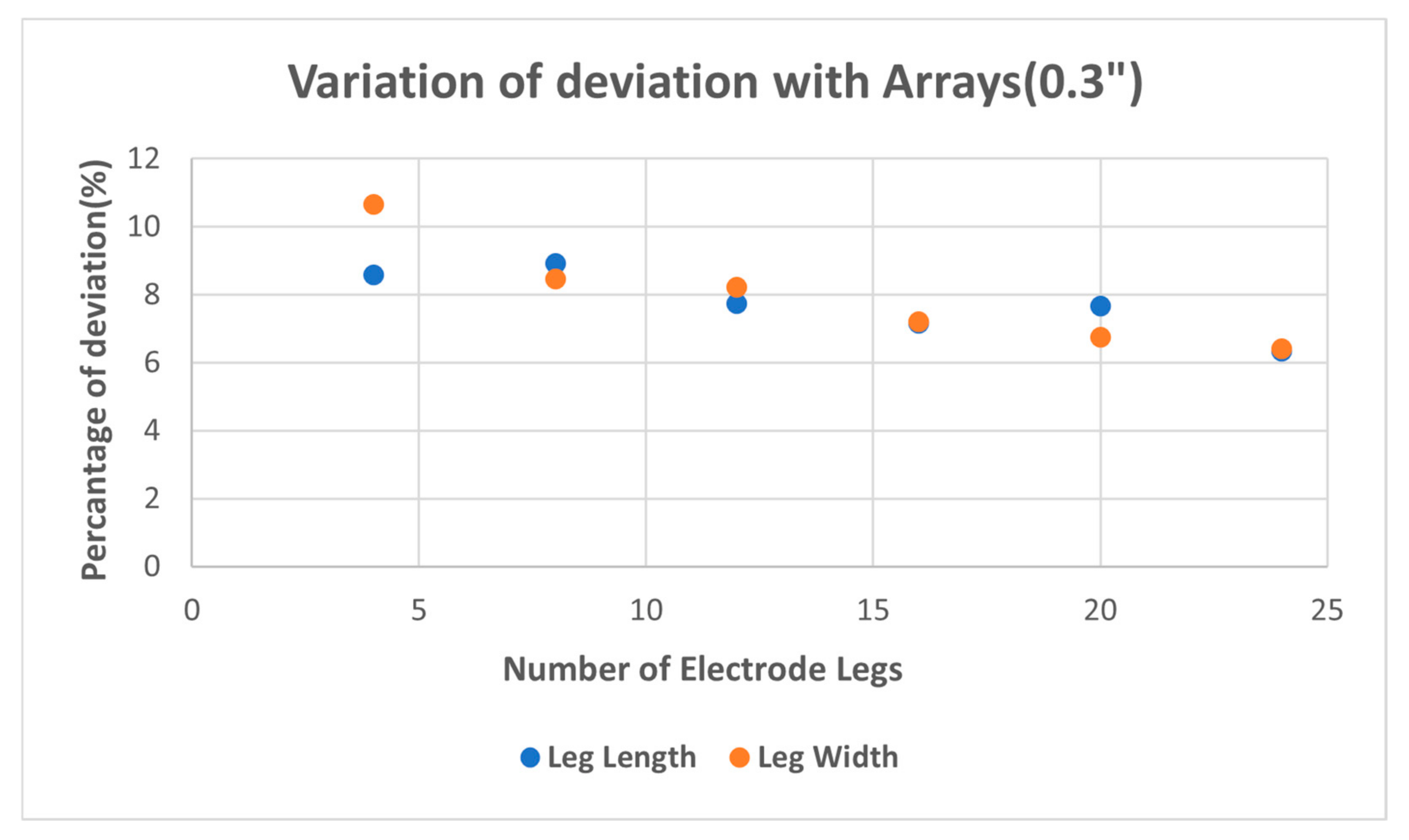
| Number of Legs | Percentage of Deviation in Arrays (%) for Height 0.2″ | Overall Percentage of Deviation in Arrays (%) for Height 0.2″ | Percentage of Deviation in Arrays (%) for Height 0.3″ | Overall Percentage of Deviation in Arrays (%) for Height 0.3″ | ||||
|---|---|---|---|---|---|---|---|---|
| Length | Width | Length | Width | Length | Width | Length | Width | |
| 4 (1 × 4) | 9.46 | 10.42 | 7.67 | 7.88 | 8.58 | 10.65 | 7.73 | 7.95 |
| 8 (2 × 4) | 9.61 | 9.61 | 8.93 | 8.47 | ||||
| 12 (3 × 4) | 7.51 | 8.06 | 7.73 | 8.22 | ||||
| 16 (4 × 4) | 6.93 | 7.04 | 7.17 | 7.21 | ||||
| 20 (5 × 4) | 6.57 | 6.38 | 7.66 | 6.76 | ||||
| 24 (6 × 4) | 5.96 | 5.81 | 6.33 | 6.41 | ||||
| Arrays of Electrode | The Average Weight of the Electrode Before Machining (gm) | The Average Weight of the Electrode After Machining (gm) | Average Carbon Accumulation per Leg (gm) |
|---|---|---|---|
| 1 × 4 | 51.91 | 54.71 | 0.6993 |
| 2 × 4 | 51.73 | 54.83 | 0.3875 |
| 3 × 4 | 52.81 | 56.58 | 0.3142 |
| 4 × 4 | 52.15 | 54.94 | 0.1744 |
| 5 × 4 | 72.36 | 76.25 | 0.1945 |
| 6 × 4 | 99.80 | 101.67 | 0.0779 |
| Arrays of Electrode | Average Weight of Electrode Before Machining (gm) | Average Weight of Electrode After Machining (gm) | Average Carbon Accumulation per Leg (gm) |
|---|---|---|---|
| 1 × 4 | 49.24 | 52.14 | 0.7250 |
| 2 × 4 | 50.02 | 53.23 | 0.4013 |
| 3 × 4 | 51.86 | 55.02 | 0.2633 |
| 4 × 4 | 50.52 | 53.26 | 0.1713 |
| 5 × 4 | 68.92 | 72.63 | 0.1855 |
| 6 × 4 | 94.32 | 96.04 | 0.0717 |
| Electrode | Sample | Length (μm) | Width (μm) | Thickness (μm) |
|---|---|---|---|---|
| Block Electrode | Sample-1 | 25,463.50 | 25,476.20 | - |
| Sample-2 | 25,463.50 | 25,463.50 | - | |
| Sample-3 | 25,463.50 | 25,463.50 | - | |
| 0.12″ Hollow Electrode | Sample-1 | 25,463.50 | 25,476.20 | 3018.841 |
| Sample-2 | 25,463.50 | 25,476.20 | 2981.047 | |
| Sample-3 | 25,476.20 | 25,463.50 | 2981.286 | |
| 0.08″ Hollow Electrode | Sample-1 | 25,476.20 | 25,463.50 | 2056.545 |
| Sample-2 | 25,476.20 | 25,463.50 | 1962.208 | |
| Sample-3 | 25,463.50 | 25,476.20 | 1962.299 | |
| 0.04″ Hollow Electrode | Sample-1 | 25,463.50 | 25,476.20 | 1056.742 |
| Sample-2 | 25,463.50 | 25,476.20 | 1113.336 | |
| Sample-3 | 25,476.20 | 25,463.50 | 1094.308 |
| Type of Electrode | Percentage of Deviation (%) at Entry Side | Percentage of Deviation (%) at the Exit Side | Overall Percentage of Deviation (%) | ||
|---|---|---|---|---|---|
| Length | Width | Length | Width | ||
| Block | 3.244% | 3.371% | 4.544% | 4.669% | 3.957% |
| 0.12″ | 3.085% | 3.355% | 3.514% | 3.641% | 3.399% |
| 0.08″ | 3.355% | 3.083% | 3.498% | 3.084% | 3.255% |
| 0.04″ | 3.095% | 1.985% | 2.795% | 1.701% | 2.394% |
Disclaimer/Publisher’s Note: The statements, opinions and data contained in all publications are solely those of the individual author(s) and contributor(s) and not of MDPI and/or the editor(s). MDPI and/or the editor(s) disclaim responsibility for any injury to people or property resulting from any ideas, methods, instructions or products referred to in the content. |
© 2025 by the authors. Licensee MDPI, Basel, Switzerland. This article is an open access article distributed under the terms and conditions of the Creative Commons Attribution (CC BY) license (https://creativecommons.org/licenses/by/4.0/).
Share and Cite
Karim, M.A.; Jahan, M.P. Effectiveness of Electrode Design Methodologies for Fast EDM Slotting of Thick Silicon Wafers. Appl. Sci. 2025, 15, 6374. https://doi.org/10.3390/app15116374
Karim MA, Jahan MP. Effectiveness of Electrode Design Methodologies for Fast EDM Slotting of Thick Silicon Wafers. Applied Sciences. 2025; 15(11):6374. https://doi.org/10.3390/app15116374
Chicago/Turabian StyleKarim, Mahmud Anjir, and Muhammad Pervej Jahan. 2025. "Effectiveness of Electrode Design Methodologies for Fast EDM Slotting of Thick Silicon Wafers" Applied Sciences 15, no. 11: 6374. https://doi.org/10.3390/app15116374
APA StyleKarim, M. A., & Jahan, M. P. (2025). Effectiveness of Electrode Design Methodologies for Fast EDM Slotting of Thick Silicon Wafers. Applied Sciences, 15(11), 6374. https://doi.org/10.3390/app15116374