Abstract
This paper provides an overview of existing theories on various modulation strategies for current-source inverters (CSI), particularly focusing on space vector modulation (SVM). The emphasis is on the development of detailed simulation models that improve understanding and allow practical application. Three important modulators are analyzed: voltage-source inverter (VSI)-derived CSI SVM modulator, direct CSI SVM modulator, and direct duty ratio CSI PWM modulator (DDPWM). These models are important for researchers and practicing engineers as they allow simulation, modification and better understanding of CSIs. This paper begins with a theoretical overview of the functionality of CSIs and presents the modulation techniques needed to develop simulation models. These modulation techniques use modular components to create complete simulation models. Application examples are provided to use the correct/valid parameters such that the operation/waveforms can be compared with the theory. Integrating established mathematical models with effective simulation tools enhances the understanding and application of CSI modulators. This method not only makes it easier to employ these CSIs instead of conventional inverter systems, but it also increases the possibility of power electronics advancements by creating better and more reliable systems.
1. Introduction
Current-source inverters (CSIs) are gaining more attention in high-power systems due to their inherent advantages in short-circuit protection, voltage boost, and reliability [1]. However, CSIs appear to be more difficult to modulate and control compared to voltage-source inverters (VSIs). Space vector modulation (SVM) is an efficient modulation technique that provides better quality waveforms, less harmonic distortion, better dynamic performance, and increased efficiency of the system.
VSIs have been studied and applied extensively in industry for many years. In contrast, there has been considerably less research work on the modulation and control of the alternative current-source/stiff inverter topology [1,2]. While quite a few publications on these topics have been made recently, there are hardly any, if any at all, simulation models or application software demo models provided that would help to run and modify the simulations to gain a better insight into the operation of the CSI.
Previous studies have described the unique benefits and challenges of CSIs in renewable energy applications. Research conducted by [3] indicates that PWM CSIs provide strong short-circuit protection, high inductor power density, and inherent voltage-boosting capability, preventing AC line faults and postponing DC link short circuits until inductor saturation. Moreover, CSIs make it possible to invert low-voltage DC sources in a single stage without the use of a boost converter [4].
Recent advancements in modulation techniques, such as the VSI-derived CSI SVM modulator, the direct CSI SVM modulator, and the direct duty ratio PWM (DDPWM) technique, have even improved the performance of inverters. These advances in SVM methods improve the reliability and efficiency of systems and support important technologies such as smart grids, renewable energy, and motor drive solutions.
VSI-derived CSI SVM modulators use the VSI space vector modulation technique to drive and control CSIs, resulting in improved performance and reduced total harmonic distortion (THD). A generalized method for adapting VSI modulation strategies to CSI has been proposed, allowing for the immediate application of sophisticated VSI techniques to CSI without additional analysis [5]. The research shows that the generalized modulation approach for CSIs can achieve a harmonic performance equivalent to that of VSIs. One study analyzes VSI topology to introduce the design of a CSI. This means the SVM strategy used for the CSI was inspired by and adapted from techniques used in VSIs, effectively creating a VSI-inspired modulation method for a CSI. The study details this adaptation in its description of the SVM scheme for the CSI. The design reduces hardware costs by 15% compared to conventional methods while maintaining over 95% efficiency [6,7].
Researchers examined carefully how the SVM approach and the zero-voltage switching (ZVS) technology work together in a CSI system intended to work with low input voltage. In the study, the proposed modulation method achieved SVM control by optimizing the energy storage mode [8,9]. An SVM model was created and applied to both VSIs and CSIs in a study that compared the two on their effectiveness in performance under different conditions [10]. The study identified the benefits of SVM over other PWM methods, including better harmonic performance and fundamental output voltage. Pham et al. [11] used SVM in CSIs to highlight the harmonic performance and operational limits of high-power medium voltage drives. Although SVM offers high control flexibility, its application in CSIs should be carefully studied to avoid harmonic distortions. A novel CSI topology was analyzed using space vector modulation, focusing on minimizing output filter components, reducing the ground leakage current, and improving efficiency [12]. A key feature is the proposed SVM strategy, which aims to minimize the THD of the injected grid current and conduction losses. In aerospace and motor drive applications, CSIs demonstrate additional benefits, such as sinusoidal voltage generation, reduced electromagnetic interference, and robust fault tolerance [13]. One study highlights the significant role of SVMs in modern CSI systems, particularly when combined with wide-bandgap (WBG) switches, which reduce losses associated with reverse-voltage-blocking devices. Consequently, CSIs can achieve efficiencies comparable to VSIs while maintaining their inherent reliability benefits [6,14] by using WBG technology. The direct CSI SVM modulator performs better than conventional PWM techniques. It improves the system’s efficiency and dynamic responses.
The DDPWM was introduced as a method that simplifies the creation of gating signals for a CSI [15]. This method allows for direct signal generation without any translation from the gating signals of VSI or without implementing the fairly complex CSI SVM. One of the key advantages of DDPWM is that each active switch has an effective switching frequency that is two-thirds of the carrier frequency, resulting in less switching loss. It is also shown that there is an isomorphic relationship between a three-phase CSI and a single-phase three-level VSI, indicating that these two systems share the same modulation characteristics. This implies that they can be analyzed and applied similarly in terms of their modulation features [16,17]. The DDPWM is a very suitable modulation method for high-power systems, as it can control the output current with less switching losses. Ming et al. also proposed one of the carrier-based pulse-width modulation (CB-PWM) techniques for CSIs to reduce the switching harmonics and minimize the common-mode voltage [18]. The others include trapezoidal PWM [19], bi-tri logic SPWM [20,21], six-step direct PWM (SS-DPWM) [22], and DDPWM previously mentioned in [15]. SS-DPWM does not have as high of a DC current utilization ratio as trapezoidal PWM. However, it has reduced switching losses.
There have been other research studies focused on CSI modulation. Instead of at fixed intervals, Lopes and Naguib suggested a dynamic SVM technique that calculates state on-times iteratively as the reference vector rotates [23]. This method reduced harmonic distortion. The study underlined the benefits of rapid dynamic response and exact control of the current magnitude and phase in CSIs by using SVM, which is essential for high-power applications. In [24], a hybrid modulation technique that combines SVM and synchronous optimal pulse-width modulation (SOPWM) was presented. This hybrid modulation technique is directly applicable to CSIs, with SVM offering better dynamic performance and THD than conventional modulation techniques. However, this technique might introduce additional complexity, and it could cause challenges in practical applications. A study suggested a new modulation technique called Active Zero-State Space Vector Modulation, developed particularly for grid-connected CSIs [25]. This one can lower high-frequency common-mode voltages by at least four times when compared to conventional SVM techniques. While [26] successfully addressed overlap-time issues, their method’s computational demands (∼15% higher than conventional SVM [2]) limit its use in real-time systems. Likewise, certain studies have proposed a novel modulation technique to remove vector deviation faults happening during the overlap instant in CSIs [27]. The suggested approach reduces these errors while producing low THD. This modulation technique may introduce higher-order harmonics (e.g., 5th, 7th) due to discontinuous current paths. Operating under both continuous and discontinuous inductor current conditions, Guo et al. [28] introduced a dual-mode modulation technique for CSIs. Despite claiming implementation simplicity, field tests revealed a steep learning curve for power electronics practitioners [2].
CSIs are appealing for high-power applications due to their inherent benefits, which include a natural voltage boost and short-circuit protection. In contrast to VSIs, their modulation and control are still less studied, in part because of the complex nature of CSI space vector modulation and the lack of available simulation models. This work fills this important gap by offering the first comprehensive, modular simulation models for the three main CSI modulation techniques:
- (1)
- VSI-derived CSI SVM modulator;
- (2)
- Direct CSI SVM modulator;
- (3)
- DDPWM (direct duty ratio CSI PWM modulator).
Since the CSI modulator is not as straightforward as the VSI modulator, the provided simulation models are designed to enable researchers and practicing engineers to better understand the CSI, connect it to existing theory, and explore its suitability for their specific applications.
Unlike prior studies that focus on theoretical analysis [7,8,9,10,11,12,13,14,15,16,17,18,19,20,21,22,23,24,25,26,27,28]; this study offers ready-to-use MATLAB/Simulink and PLECS models, empowering researchers and engineers to evaluate, modify, and optimize CSI performance. By integrating these models with comprehensive fundamentals and comparative performance metrics (e.g., THD below 5% for all methods), this work accelerates the adoption of CSIs in smart grids, industrial drives, and renewable energy systems.
This work is divided into a few parts. First, a quick theory of the CSI operation and basic relations are provided. Then, the theory of the CSI modulators needed for the simulation models is explained in detail with the building blocks. The CSI modulators are then shown by joining the building blocks of each model to form the final simulation model so that the reader can use them. Finally, the application examples are shown to ensure that proper and allowed limits are applied. This enables the comparison between actual performance and theoretical analysis and design. To improve understanding of the operation of the CSI and simplify simulations, the suitable ranges for variables such as VDC, VAC, modulation index (m), switching frequency (fSW), and filter parameters are presented.
1.1. CSI Theory Review
Voltage-source inverter space vector modulation strategies have been extensively studied and applied in power electronics. The fundamental advantage of VSI SVM is a two-pole inverter state that is, in essence, less complicated than that of the CSI, which has three states for its inverter pole. As shown in [29,30], this inherent simplicity of VSI SVM, combined with its well-established characteristics, makes it possible to use and adapt it to drive the CSI efficiently, which may boost its performance and advantages.
This method is feasible and straightforward to implement. The basic topology under consideration is illustrated in Figure 1 [31].
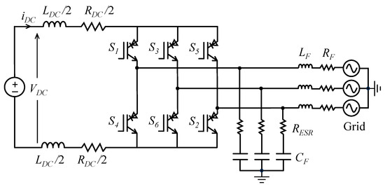
Figure 1.
Grid-connected CSI topology. The circuit includes a DC link inductor at the input and an output low-pass filter connected to the grid at the output.
The VSI operates with three switches active at any given time. In contrast, the CSI operates with only two switches active simultaneously. The fundamental vectors of the CSI are orthogonal to the missing phase vector; for instance, vector bc is orthogonal to vector a, ca is orthogonal to b, and ab is orthogonal to c [32]. Consequently, the base vectors of the CSI are phase-shifted by π/6 (or 30°) when compared to a VSI.
The CSI space vectors, corresponding to active switching states, align with the vertices of a regular hexagon and have the magnitude specified in Equation (1):
Similar to the VSI operation [29], the reference space vector in the CSI [32] can be represented as a complex summation of two adjacent base vectors. For Sector 1, the calculation proceeds as follows:
where denotes the reference of the input phase’s current fundamental component; and represent the duty cycle of base vectors , , and zero state ( indicates shorted phase leg), respectively. The notation in Figure 2 is such that the first letter denotes the positive rail and the second letter, the negative rail. For instance, means that a is positive and is negative (S1S6). The modulation index m is defined as the ratio of the peak phase current to the DC link current.
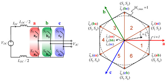
Figure 2.
Basic CSI current vectors. Vectors (e.g., ab) represent switching states with magnitude . Asterisks denote reference values.
By neglecting converter losses and applying the principle of input/output power balance, the modulation index can also be expressed as [31]:
This leads to an important constraint between the input source voltage and load voltage:
where ϕ is the phase shift between the fundamental component of the pole output current (square wave current) and the load (AC source) voltage.
1.2. Key Assumptions and Operational Conditions
In this work, the load is purely resistive, eliminating the need for grid connection control (PLL), which is not the focus of this study. However, since the filter inductor’s reactance is significantly higher than the load resistance at the switching frequency (tens of kHz), the analysis and simulation will also remain highly accurate and applicable to the grid-connected CSI. For instance, with and a switching frequency of , the reactance () is , which is significantly larger than the load resistance used in the simulation.
This study will assume the converter’s continuous mode of operation. This means the DC link inductor current will not drop to zero and will remain relatively constant for the example shown in the application section.
Please note that the reference space vector used in the synthesis is constant during the switching period, which means the amplitude of the sinusoidal load currents remains unchanged. This condition can be achieved in practice by maintaining a high switching frequency.
1.3. Additional Design Equations for CSI
The following equations are critical for proper CSI design [31].
DC link current maximum ripple:
where , is the input voltage, and is the DC link inductor.
Output filter (LC) capacitor RMS current:
Determining the maximum DC link ripple and the low-pass output filter’s capacitance current precisely is essential to avoiding design errors in high-power applications where substantial ripple or capacitor stress could cause failure.
2. VSI-Derived CSI SVM Modulator
An alternative approach to simplifying the use of space vector modulation for CSI, which involves complex calculations, is to use a VSI modulator that emulates VSI SVM. The modulator’s hardware option is especially widely used in aerospace applications to avoid software complexity, particularly software certification.
2.1. Modulation Index Relationship Between VSI and CSI
The vectors for the CSI, as shown in Figure 2 above, are tabulated using the notation of upper switches and lower switches [7,33]. For instance, I1 (100, 001) and I6 (100, 010) as shown later in Figure 5b below.
The VSI modulation index is defined as the ratio of the maximum of the phase voltage and half of the DC link voltage:
with a theoretical maximum of:
whereas the maximum value of the CSI modulation index is:
This limit in Equation (11) is easily understood because if the phase stays connected to the IDC rail for the duration of the pulse period or if there is no freewheeling, the local mean value of the phase current can assume a maximum of the value of the current IDC as shown in Equation (4) [32].
From Equations (10) and (11), the relationship between the modulation indices of the CSI and the VSI can be determined as shown in Equation (12) below:
2.2. Switch-State Mapping and Implementation
A critical aspect of this modulator is the clear mapping between VSI switching states and CSI switching states as originally introduced and explained by [7] as shown in Table 1 below, while Figure 5 illustrates the switch operation pattern [33]. Researchers and engineers can evaluate and improve the performance of these inverters in a variety of applications due to this mapping, which enables simulation models to accurately represent the switching behavior of CSIs. Consistency between theory and practice is ensured by the table’s notation, which includes switch states (e.g., S1, S2), corresponding to the simulation models and theoretical framework offered in this study.

Table 1.
VSI analog input as variables to the CSI vectors.
The relationships for the CSI vectors using VSI can now be determined from Table 1 and simplified using the Boolean Algebra AND-Distributive Law, which states that as shown in Equation (A1) in Appendix A.
The equations from (A1) are used in PLECS Blockset 4.9, shown below in Figure 3. This method uses reliable SVM techniques from VSIs, which have been adapted for CSI operations, simplifying the modulation procedure. The analog input signals obtained from the VSI modulator are utilized to produce the necessary switching patterns for the CSI [7]. This method reduces the complexity of the CSI modulation process. The figure highlights the fundamental components of the modulator, including the analog input signals and the associated switching patterns, providing a clear visual description of the application of VSI-derived modulation to the CSI.
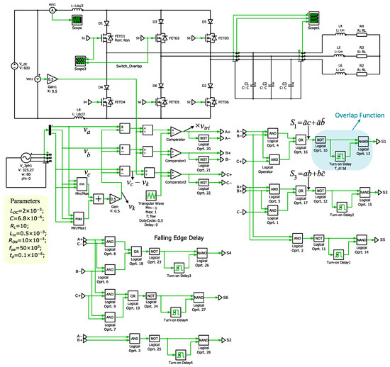
Figure 3.
CSI modulator based on analog space vector modulation input.
2.3. Overlap Time Consideration
In analogy with the exclusive dead time for the VSI, the CSI requires an overlapping time (inclusive time) of the upper and lower switches, as indicated below. Figure 3 also shows the detailed implementation of the overlap control mechanism for the CSI MOSFETs. The overlap time is very important to guarantee the switching sequence integrity and good switching state transitions, thus improving the generic reliability and performance of that CSI. This configuration ensures safe and efficient switching, mitigating the risk of an open circuit (voltage spikes) for a current source during the overlap period.
Figure 4 presents the simulation results for a CSI using a VSI-derived CSI SVM. The figure displays waveforms for the output filter’s capacitor voltage, the output current before the low-pass filter, and the load current. It demonstrates the effectiveness of the modulation technique in generating almost pure sinusoidal output currents from the CSI. The close match between the simulated current waveform and the desired sinusoidal shape indicates the system’s good performance.
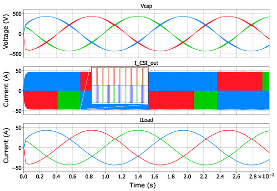
Figure 4.
CSI with analog VSI as input. Red represents phase 1, green phase 2, and blue phase 3 of the CSI.
3. Direct CSI SVM Modulator
The direct CSI (or VSI) SVM space vector modulation requires considerably more computational power for both simulations and more complex hardware implementation. The advantage of this approach is the flexibility in vector placement, compared to the lack of flexibility in the previous case. In the available literature, various CSI strategies have been discussed. In this paper, the space vector modulation and the sequence are shown in Figure 5 below [34]. The space vectors and switching sequences that form the basis of direct CSI SVM modulation are shown in Figure 5a. It represents the arrangement of current vectors in the hexagonal plane and their switching states, while Figure 5b indicates the different combinations of switches required to generate these vectors. The goal here is to obtain the desired current vector in the appropriate switching order, which is critical for efficient modulation.
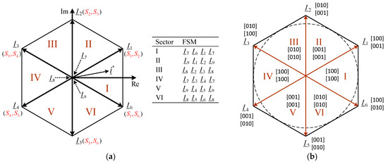
Figure 5.
(a) Space vectors of CSI and sequences of FSM; (b) basic space vectors with different switch combinations. Asterisks denote reference values.
Major Simulation Blocks Based on Top-Level Drawing
The modulator was implemented in MATLAB/Simulink 2023b with PLECS Blockset 4.9 (see Figure 6). Each of the main blocks shown here has multiple sub-blocks. The CSI parameters stay the same as those used in the previous approach.
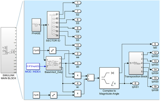
Figure 6.
Simulink main block and its internal subblocks.
The top-down building block graphic below is meant to improve understanding of how to combine the components. The simulation model should be built from the bottom up so that every block operates as an independent entity in Simulink and PLECS.
- Phase Generation for Standalone (Off-Grid RL) Operation:
Figure 7 shows the phase generation and duty-cycle calculation block for the standalone CSI modulator. The integrator (with an initial phase of and reset at ) generates the fundamental phase angle used to derive sinusoidal reference signals. Below this, the block implements Equations (2) and (3) to compute the duty cycles () for Sector 1’s base vectors (ab, ac, aa). Key operations include:
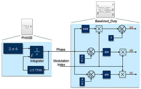
Figure 7.
Phase-angle generator and duty-cycle calculation for Sector 1. The integrator (initialized at ) outputs the phase (), while the block on the right computes vector duties () via Equations (2) and (3).
- Trigonometric mapping: The reference phase is processed via terms to determine vector weights.
- Modulation Index Scaling: The output () adjusts the duty cycle to meet the desired current amplitude (Equation (4)).
This modular block is the fundamental component of the direct CSI SVM modulator. It allows for real-time generation of the reference current with a configurable modulation index and frequency.
- 2.
- Modulation index and the required frequency as the inputs.
- 3.
- Basic vector duty calculation in Sector 1:
Figure 7 illustrates this process, utilizing Equations (1)–(3). This block calculates the duty cycles for the CSI’s switching states based on the desired output current vector.
- 4.
- The Simulink Block Complex-to-Magnitude Angle:
This block is used to find the amplitude and phase of the CSI from the complex function Equations (5) and (6) above, implemented in step 3 as seen in Figure 6. Determining the total current supplied by the inverter requires knowledge of the amplitude and phase angle of the current vector. Therefore, this block assists in calculating these values.
- 5.
- Sector identification block, sector ID:
Figure 8 shows Simulink building blocks, which are fundamental elements of model-based design and simulation. As shown in Figure A1 in Appendix A and Figure 6, these blocks are inside the top-level Simulink block. The sector identification block in Figure 8 is essential for identifying the proper switching patterns necessary to achieve the desired output current vector for a CSI. This identification provides the necessary angles to calculate duty cycles of the inverter switches required for successful modulation.
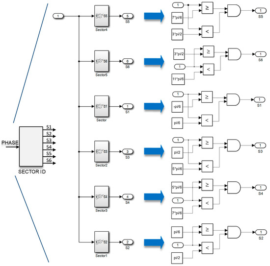
Figure 8.
Sector identification block. This module determines the sector (1–6) in the hexagonal current vector plane where the reference vector resides, enabling the selection of appropriate switching sequences for the CSI SVM modulator.
- 6.
- Basic Vector Sector Transposition:
This block rotates the base vectors calculated in Equations (1) and (2), as shown in Figure 9. It is quite important in controlling the inverter’s switching states since it simplifies the identified sector of the current vector. This helps to determine the switching states. For example, vectors in Sector 2 are mapped to Sector 1 equivalents via a phase shift. This transformation makes it easier to calculate the switching states. By shifting the reference point of the current vector, the process simplifies how the right switching sequences are identified, which helps in choosing the states needed to produce the desired output current vector.
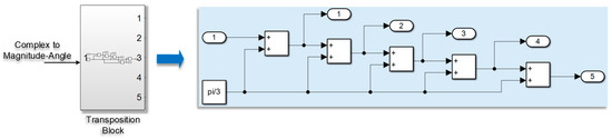
Figure 9.
Basic vector sector transposition block used to rotate base vectors for simplified sector identification.
Figure 10 illustrates the PLECS Blockset main block and its internal subblocks integrated within MATLAB/Simulink (see Figure A1), providing a detailed simulation model for CSI modulation. The image emphasizes a modular design of the simulation in which subblocks generate modulation signals, manage switching states, and control CSI general operation. Using PLECS together with MATLAB/Simulink makes the seamless simulation of control algorithms and power electronics circuits possible, enabling the analysis of SVM approaches. The model confirms correct switching patterns that reduce harmonic distortion and improve output current quality by extracting modulation signals from the reference space vector.
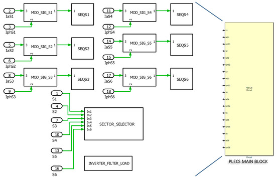
Figure 10.
The PLECS Blockset main block and its internal subblocks are integrated within MATLAB/Simulink. See Figure 6 for the top-level Simulink diagram.
- 7.
- The modulation signal extracted from the reference space vector in sectors 1–6:
Figure 11 shows how reference space vectors are converted into modulation signals (S1–S6). These blocks are critical for extracting modulation signals from the reference control inputs that define the desired current waveforms for the CSI. The extracted signals are needed to ensure that the output currents closely match the desired sinusoidal waveforms and to control the inverter’s switching states. The figure depicts the way these blocks are used in the simulation and the method of converting the reference space vector into the necessary modulation signals. It is very important to obtain a properly working and efficient CSI system. This process affects the quality of the output current and the overall performance of the inverter. The modular design of the modulation method eliminates the compatibility problem for different CSI modulation designs and control strategies. This flexibility makes these blocks essential tools for studying and improving CSI modulation in power electronics applications.
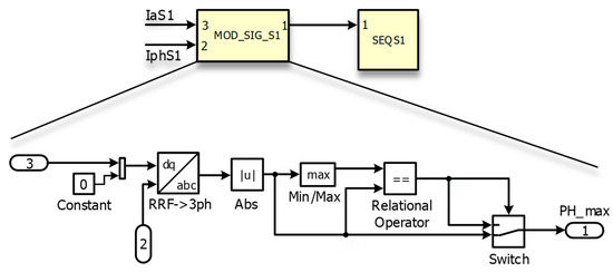
Figure 11.
Modulating signal extraction blocks.
- 8.
- The sequencer is based on Sawtooth PWM (unlike the previous method with triangular PWM) and implements the patterns shown in Figure 5a above:
This sequencer and its blocks, as seen in Figure 12, use a sawtooth waveform where the PWM output duty cycles are computed from the intersection of the sawtooth with reference signals. The sequencer efficiently manages the duration for which each inverter switch remains active by varying the height of these reference signals, therefore enabling the creation of output waveforms that closely approximate desired sinusoidal forms.
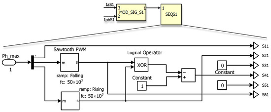
Figure 12.
Sequencer implementation based on Sawtooth PWM, enabling efficient control of inverter switching durations.
Figure 13 shows the modulation waveforms of the control inputs from the reference for generating the CSI’s switching patterns, depicting correct sector transition and duty-cycle distribution.
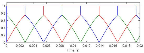
Figure 13.
Modulation signals (S1–S6) for the direct CSI SVM modulator, implementing the vector sequences of Figure 5a. Pulse widths correspond to vector dwell times ().
Figure A2 (Appendix A) details the symmetric SVM switching sequences implemented in the CSI simulation model, where each sector (1–6) follows predefined combinations of active vectors (e.g., ab, ac) and zero states (aa, bb, cc) to synthesize reference currents with minimum THD. The sequences enforce symmetry (even vector distribution per switching period) and a fixed 200 ns overlap time (shaded) for safe commutation, directly validating the modular simulation approach. These patterns enable users to verify sector transitions against theoretical predictions (see Section 2), experimentally adjust dwell times, and benchmark THD performance across modulation techniques, while serving as a foundation for custom SVM implementations.
- 9.
- The sector selector and the state machine:
Figure A3 in Appendix A shows the detailed subblocks of the selector block. The sector selector block is quite important in SVM for a three-phase CSI in deciding which of the six sectors the reference space vector currently resides in. This identification is necessary to enable the correct inverter switching states to generate the desired output. Figure 8 shows the full design of the sector selector, in which a full finite state machine is shown.
By coordinating the timing and sequence of inverter switching states, the state machine in SVM ensures the true synthesis of the desired current waveform for the highest performance and least distortion.
- 10.
- The CSI circuit uses the same values as the VSI-derived CSI SVM modulator:
The comparative analysis uses the same basic component values of the CSI circuit displayed in Figure 3 from the VSI-derived CSI SVM modulator. This guarantees constant parameter values among several modulation methods under the same operational settings, making a proper comparison of the performance characteristics for these methods.
Figure 14 shows the implementation of the SVM for Sector 1. Figure 14a illustrates the unfiltered current waveforms for Sector 1 at the top. The red waveform denotes phase 1, the green waveform indicates phase 2, and the blue waveform corresponds to phase 3 of the CSI. The total of the phase currents is equal to zero, as seen in Figure 14b. This validates the pattern for the direct duty ratio CSI SVM modulator. This illustration presents an enlarged depiction of the upper waveform displayed in Figure 14a. Sector 1 SVM pulses are illustrated below the unfiltered current waveform. The lower waveform in Figure 14a demonstrates nearly pure sinusoidal current waveforms of the three-phase CSI inverter.
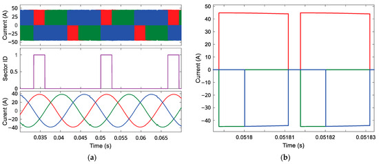
Figure 14.
Output current waveforms of the CSI using direct space vector modulation: (a) Unfiltered phase currents (red: phase 1, green: phase 2, blue: phase 3) and filtered sinusoidal output currents below Sector ID; (b) Sum of phase currents validating zero-sequence balance.
4. Direct Duty Ratio CSI PWM
This modulator produces PWM signals for a three-phase system utilizing two triangular carriers and three reference signals. This method decreases losses caused by an effective switching frequency of two-thirds of the carrier frequency at each active switch by allowing for the direct creation of CSI gating signals from VSI signals and using overmodulation (see Figure 15).
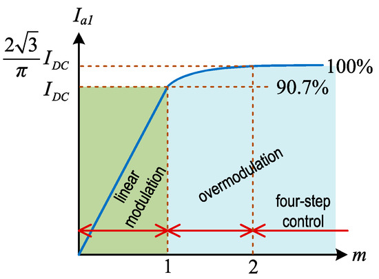
Figure 15.
Overmodulation capability of DDPWM [15].
The CSI topology can be represented as a Single-Pole Triple-Throw Switch (SPTT). Figure 16a shows a simple circuit diagram of a three-phase CSI to illustrate the synthesis of the output phase currents. It determines the three phases (max, medium, min) according to the magnitude of the output currents (). This simplifies the analysis by focusing on the maximum (max), medium (mid), and minimum (min) current phases at any given time. Figure 16b shows the waveforms of the maximum () and minimum () currents when balanced three-phase sinusoidal command currents () are applied. The maximum phase current is always positive, and the minimum phase current is always negative. Thus, the sum of the currents of the three phases will be equal to zero. These waveforms indicate the lowest and highest phase current values needed to create output current using the DDPWM method.
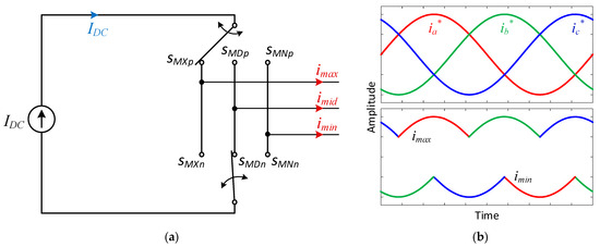
Figure 16.
(a) CSI model using SPTT switches, (b) the max phase current imax and the min phase current imin.
Where SMXp and SMXn represent the maximum and minimum values of the three-phase currents.
The relevant relations for the DDPWM operation are given below [15]:
Figure 17 graphically shows Equations (15) and (16), therefore showing the generation of the minimum (SMNn) and maximum (SMXp) phase currents in the DDPWM system. The waveforms show the timing signals TMDp1, TMDp2, TMDn1, and TMDn2 together with the relationship between the input DC current (IDC), the maximum (IMAX), and minimum (IMIN) thresholds. The timing signals control the duration of the related currents during each switching cycle. A proper output current waveform depends on the accurate decision for SMXp and SMNn.

Figure 17.
Synthesis of max phase current on the left and min phase current on the right.
Figure 18a shows a block diagram of the DDPWM, highlighting its key components. The Max-Min Identifier block determines the maximum and minimum phase currents. The values are then fed into the Upper and Lower SPTT Selectors, which produce the required gating signals according to the switching strategy. This direct approach simplifies the modulation process relative to alternative CSI modulation techniques. Figure 18b shows the subblocks of the simulation circuit that implement the DDPWM technique. The main CSI circuit is identical to that shown in Figure 3.
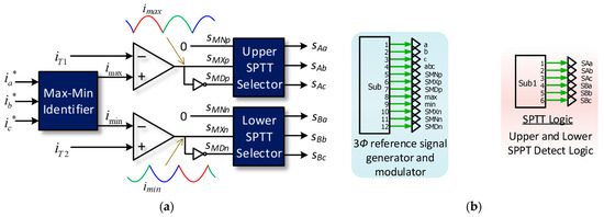
Figure 18.
DDPWM implementation: (a) Top-level block diagram; (b) Subblocks for max–min identification and SPTT switching. Combines carrier-based modulation [18] with SPTT logic [15,16].
Figure 19 and Figure A4 in Appendix A illustrate subcircuits in Figure 18b that generate DDPWM. The three-phase reference signals (a, b, and c) and the DDPWM technique are implemented in the simulation model as shown in Figure 19. This figure describes the DDPWM technique and how the simulation produces the three-phase reference signals (a, b, and c).
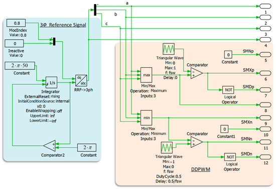
Figure 19.
3Ф reference signals (a, b, and c) and DDPWM signal generation logic. The modulator implements Equations (13)–(16) to derive switching signals directly from current references, eliminating VSI signal conversion.
Figure A4 in Appendix A shows the PLECS model of the DDPWM modulator for the CSI. The graphic illustrates a detailed implementation of the logic necessary to generate switching signals. The Max-Min Identifier, Upper and Lower SPTT Selectors, and logic gates that determine each phase’s final switching states are all critical components. This design’s versatility makes it simple to learn and adapt to new applications.
The simulation results presented in Figure 20 show the effectiveness of the DDPWM method for the three-phase CSI. This new carrier-based PWM technique, as described in [15], creates gating signals directly using two triangular carriers and three reference signals, therefore removing the need for translation from VSI gating signals as mandated by existing approaches. The simulated waveforms show almost pure sinusoidal output currents under a balanced load state, therefore confirming the simplicity and attractiveness of this approach. The DDPWM approach provides an alternative solution for controlling CSI by means of simple implementation and better efficiency.
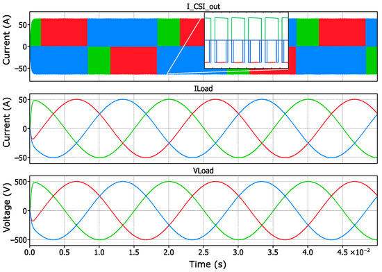
Figure 20.
CSI output current, load current, and voltage after the output filter. The red waveform denotes phase 1, the green waveform indicates phase 2, and the blue waveform corresponds to phase 3 of the CSI.
5. Simulation Examples
The parameters listed in Table 2 were calculated for simulation examples. Three different modulation methods were implemented using these parameters.
Table 2.
Calculated parameters applied to all three CSIs.
In Table 2, the DC link input voltage VDC was calculated using Equation (6). Similarly, the average DC link current can be calculated using Equation (17) below.
Next, the value of LDC was selected by using Equation (7) and choosing a 10% ripple current, which was A. Please note that the switching and conduction losses were ignored for all the calculations and simulations for the sake of simplicity.
Table 3 presents the total harmonic distortion values for three different PWMs. The table indicates that the THD values are quite low. The waveforms illustrate the potential of these modulation techniques in terms of minimizing THD. In addition, the calculated values correspond closely with the simulation values. For instance, the CSI modulation index shows a discrepancy of only 0.3% compared to the simulation value, with the calculated value being 0.9 and the simulated value being 0.8725 for the VSI-derived CSI SVM modulator case.
Table 3.
Comparative evaluation of CSI modulation techniques: THD, efficiency, and key characteristics under standardized conditions (VDC = 470 V, fsw = 50 kHz, RL= 21.16 Ω).
Table 3 compares the efficiency and THD of the three modulation techniques under the same simulation conditions. It is important to note that these results reflect idealized component behavior to isolate the impact of modulation strategies. Despite these controlled conditions, the models presented in this paper provide consistent comparisons of THD and efficiency across three modulation techniques under idealized conditions (e.g., lossless components, perfect switching). Although these findings demonstrate the theoretical potential of each approach, practical implementations may vary due to parasitic effects, non-linearities, or equipment limitations. The key objective of the models, therefore, is to provide a consistent baseline for researchers and engineers to assess modulation techniques prior to hardware prototyping investment.
Figure 21a shows the trade-offs between harmonic performance and the modulation index, while Figure 21b shows the efficiency as a function of the modulation index. All modulation methods achieve a total harmonic distortion of less than 5%, which is below the limits set by several standards [35,36]. However, as indicated in Table 3 and Figure 21, the DDPWM method obtains an even lower THD under the same conditions and parameters. Figure 21a demonstrates that DDPWM achieves excellent waveform quality, with THD values significantly lower than those of VSI-derived SVM (0.42% vs. 1.72% at m = 0.9). This is supported by the efficiency graph in Figure 21b, which shows that DDPWM has an advantage in energy conversion (97% efficiency vs. 94% for VSI-derived SVM at the same ), resulting from a 33% decrease in effective switching frequency. Although direct SVM has trade-offs regarding these metrics (1.1% THD, 95% efficiency), the combined results indicate an important design principle: systems tolerant of medium harmonics (e.g., motor drives) can choose direct SVM, whereas applications that have strict THD standards (e.g., grid-connected inverters) could prefer DDPWM. These efficiency and THD values emphasize how important it is to optimize both factors when choosing modulation strategies.
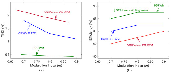
Figure 21.
The relationship between modulation index and (a) THD, (b) efficiency for VSI-derived CSI SVM, direct CSI SVM, and DDPWM modulation techniques.
6. Conclusions
This work presents three key current-source inverter modulation techniques: VSI-derived CSI SVM, direct CSI SVM, and direct duty ratio CSI PWM. It also includes extensive simulation models and analyzes the fundamentals of each modulation strategy in detail. These models address a significant gap in the availability of simulation models for CSI modulation and the existing theory, a complexity sometimes overlooked in comparison to the relatively simple VSI method. For those working with CSI technology, the straightforward models and comprehensive simulations presented here constitute a great resource.
The modular structure of the blocks presented in this study will allow engineers and researchers to adapt them easily to similar applications. This study shows how to analyze the performance of CSIs in practice and how to achieve even better results when the calculations and predictions, in theory, are combined with the necessary mathematical approaches.
Table 3 and Figure 21 demonstrate that each modulation technique has its own unique advantages. VSI-derived SVM is suitable for simplicity (94% efficiency, 1.72% THD), direct SVM is suitable for balanced performance (95% efficiency, 1.1% THD), and DDPWM is suitable for optimal metrics (97% efficiency, 0.42% THD). The simulation results show that all three methods comply with the THD grid standards below 5%. This shows the ability of these techniques to improve the efficiency and reliability of power electronic systems, particularly in high-power conditions, where CSIs are increasingly implemented. By providing models for all three approaches, this work enables both academic research and industrial applications to benefit from the practical applicability of the models, which is further improved by the inclusion of comprehensive parameter selection advice and waveform comparisons.
Future work will focus on experimental validation of these techniques at different power levels. Integration with wide-bandgap devices and application-specific optimizations for renewable energy systems are also valuable directions. This detailed study provides the necessary tools for its wider use in power electronics systems.
Author Contributions
Conceptualization, G.E. and E.N.; methodology, G.E. and E.N.; software, G.E. and E.N.; validation, G.E. and E.N.; formal analysis, G.E. and E.N.; investigation, G.E. and E.N.; resources, G.E. and E.N.; writing—original draft preparation, G.E. and E.N.; writing—review and editing, G.E. and E.N.; visualization, G.E. and E.N.; project administration, G.E. and E.N. All authors have read and agreed to the published version of the manuscript.
Funding
This research received no external funding.
Institutional Review Board Statement
Not applicable.
Informed Consent Statement
Not applicable.
Data Availability Statement
The raw data supporting the conclusions of this article will be made available by the authors on request.
Acknowledgments
The authors gratefully acknowledge Plexim GmbH for providing a sponsored academic license of PLECS software to Bilecik Seyh Edebali University, which facilitated the simulations presented in this work.
Conflicts of Interest
Author Erol Nikocevic was employed by the company Data Technologies Inc. The remaining authors declare that the research was conducted in the absence of any commercial or financial relationships that could be construed as a potential conflict of interest.
Abbreviations
The following abbreviations are used in this manuscript:
| CSI | Current-source inverter |
| DDPWM | Direct duty ratio pulse-width modulation |
| FSM | Full Wave Symmetrical Modulation |
| PLL | Phase-locked loop |
| PWM | Pulse-width modulation |
| SPTT | Single-Pole Triple-Throw Switch |
| SOPWM | Synchronous Optimal Pulse-Width Modulation |
| SS-PWM | Six-step direct PWM |
| SVM | Space vector modulation |
| THD | Total harmonic distortion |
| VSI | Voltage-source Inverter |
| ZVS | Zero-voltage switching |
Appendix A
Appendix A.1. Mapping VSI States to CSI Switches via Boolean Reduction
Appendix A.2. Top-Level MATLAB/Simulink and PLECS Blocks
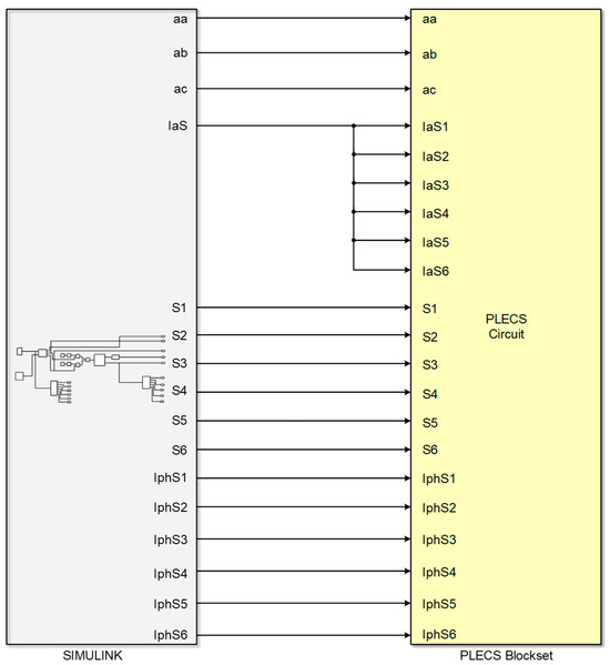
Figure A1.
Top-level MATLAB/Simulink and PLECS blocks.
Appendix A.3. Symmetrical SVM Patterns for All Six Sectors
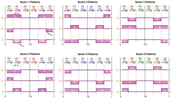
Figure A2.
Detailed switching sequences for symmetrical SVM implementation of the CSI. Sector 1–3 patterns, Sector 4–6 patterns, showing gate signals (S1–S6) and current paths.
Appendix A.4. Finite State Machine Implementation for Vector Sector Identification
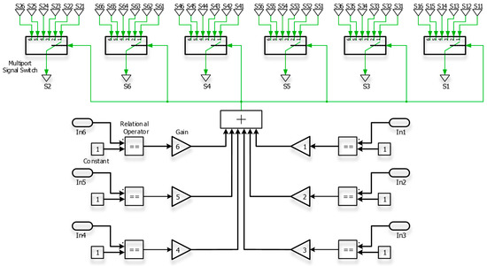
Figure A3.
Sector selector and the state machine.
Appendix A.5. SPTT Selector Implementation for Direct Duty Ratio Control
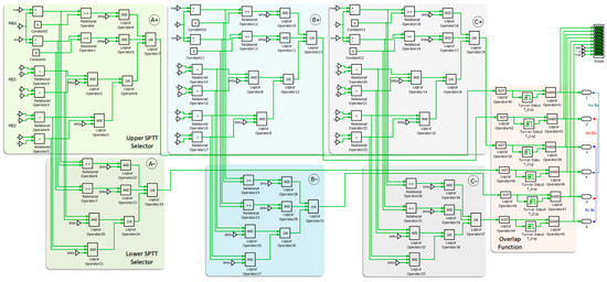
Figure A4.
Complete logic implementation of the SPTT selector for DDPWM.
References
- Marignetti, F.; Di Stefano, R.L.; Rubino, G.; Giacomobono, R. Current Source Inverter (CSI) Power Converters in Photovoltaic Systems: A Comprehensive Review of Performance, Control, and Integration. Energies 2023, 16, 7319. [Google Scholar] [CrossRef]
- Holmes, D.G.; Lipo, T.A. Pulse Width Modulation for Power Converters: Principles and Practice, 1st ed.; Wiley-IEEE Press: Hoboken, NJ, USA, 2003. [Google Scholar]
- Sahan, B.; Araújo, S.V.; Nöding, C.; Zacharias, P. Comparative Evaluation of Three-Phase Current Source Inverters for Grid Interfacing of Distributed and Renewable Energy Systems. IEEE Trans. Power Electron. 2011, 26, 2304–2318. [Google Scholar] [CrossRef]
- Sahan, B.; Vergara, A.N.; Henze, N.; Engler, A.; Zacharias, P. A Single-stage PV module integrated converter based on a low-power current-source inverter. IEEE Trans. Ind. Electron. 2008, 55, 2602–2609. [Google Scholar] [CrossRef]
- Zmood, D.N.; Holmes, D.G. A generalised approach to the modulation of current source inverters. In Proceedings of the IEEE 29th Annual Power Electronics Specialists Conference, Fukuoka, Japan, 17–22 May 1998; pp. 739–745. [Google Scholar]
- Wang, W.; Li, X.; Rui, S.; Xia, X. Three-phase boost-stage coupled current source inverter concept and its space vector modulation. Front. Energy Res. 2023, 10, 1–11. [Google Scholar] [CrossRef]
- Espinoza, J.R.; Joos, G. Current-source converter on-line pattern generator switching frequency minimization. IEEE Trans. Ind. Electron. 1997, 44, 198–206. [Google Scholar] [CrossRef]
- Di Stefano, R.; Marignetti, F.; Pellini, F. Design, Simulation and Performance of a CSI Converter for Grid-Connected or Islanded Microgrids with High Step-Up Capability in PV Applications. Energies 2024, 17, 4787. [Google Scholar] [CrossRef]
- Ma, D.; Jiang, J. A Current Source Inverter with Zero-Voltage-Switching for Low-Input Voltage PMSM Drive Application. Electr. Eng. 2023, 105, 3161–3173. [Google Scholar] [CrossRef]
- Pradeepa, S.; Kumar, S.P.; Prakash, G. Adoption of SVPWM Technique to CSI and VSI. In Proceedings of the IEEE 3rd International Conference for Convergence in Technology (I2CT), Pune, India, 6–8 April 2018; pp. 1–6. [Google Scholar]
- Pham, D.C.; Huang, S.; Huang, K. Modeling and Simulation of Current Source Inverters with Space Vector Modulation. In Proceedings of the IEEE International Conference on Electrical Machines and Systems, Incheon, Republic of Korea, 10–13 October 2010; pp. 320–325. [Google Scholar]
- Lorenzani, E.; Immovilli, F.; Migliazza, G.; Frigieri, M.; Bianchini, C.; Davoli, M. CSI7: A Modified Three-Phase Current-Source Inverter for Modular Photovoltaic Applications. IEEE Trans. Ind. Electron. 2017, 64, 5449–5459. [Google Scholar] [CrossRef]
- Fidone, G.L.; Migliazza, G.; Carfagna, E.; Benatti, D.; Immovilli, F.; Buticchi, G.; Lorenzani, E. Common Architectures and Devices for Current Source Inverter in Motor-Drive Applications: A Comprehensive Review. Energies 2023, 16, 5645. [Google Scholar] [CrossRef]
- Riegler, B.; Hartmann, M. Design and Implementation of 3 kW All-SiC Current Source Inverter. Electronics 2025, 14, 522. [Google Scholar] [CrossRef]
- Choi, N.-S.; Lee, K.-W.; Han, B.-M. A Novel Carrier Based PWM for Current Source Converter. In Proceedings of the IEEE 7th International Power Electronics and Motion Control Conference, Harbin, China, 2–5 June 2012; pp. 1945–1950. [Google Scholar]
- Li, Y.; Ding, L.; Li, Y. Isomorphic relationships between voltage-source and current-source converters. IEEE Trans. Power Electron. 2019, 34, 7131–7135. [Google Scholar] [CrossRef]
- Blaabjerg, F. (Ed.) Control of Power Electronic Converters and Systems: Volume 3; Academic Press: Cambridge, MA, USA, 2021; ISBN 0128194324. [Google Scholar]
- Ming, L.; Ding, W.; Yin, C.; Xin, Z.; Loh, P.C. A Direct Carrier-Based PWM Scheme with Reduced Switching Harmonics and Common-Mode Voltage for Current Source Converter. IEEE Trans. Power Electron. 2021, 36, 7783–7796. [Google Scholar] [CrossRef]
- Nonaka, S.; Neba, Y. New GTO Current Source Inverter with Pulsewidth Modulation Control Techniques. In Proceedings of the IEEE Annual Meeting Industry Applications Society, Toronto, ON, Canada, 29 September–4 October 1985; pp. 442–447. [Google Scholar]
- Ding, L.; Li, Y.W. Simultaneous DC Current Balance and CMV Reduction for Parallel CSC System with Interleaved Carrier-Based SPWM. IEEE Trans. Ind. Electron. 2020, 67, 8495–8505. [Google Scholar] [CrossRef]
- Ding, L.; Quan, Z.; Li, Y.W. General Bi-Tri Logic SPWM for Current Source Converter with Optimized Zero-State Replacement. IEEE Trans. Power Electron. 2021, 36, 11372–11382. [Google Scholar] [CrossRef]
- Bai, Z.; Ruan, X.; Zhang, Z. A Generic Six-Step Direct PWM (SS-DPWM) Scheme for Current Source Converter. IEEE Trans. Power Electron. 2010, 25, 659–666. [Google Scholar]
- Lopes, L.A.C.; Naguib, M.F. Space Vector Modulation for Low Switching Frequency Current Source Converters with Reduced Low-Order Noncharacteristic Harmonics. IEEE Trans. Power Electron. 2009, 24, 903–910. [Google Scholar] [CrossRef]
- Gnanasambandam, K.; Rathore, A.K.; Edpuganti, A.; Sirinivasan, D. Hybrid SVM-SOPWM modulation of current-fed three-level inverter for high power application. In Proceedings of the IEEE Industry Applications Society Annual Meeting, Cincinnati, OH, USA, 1–5 October 2017; pp. 1–8. [Google Scholar]
- Gao, H.; Mahmud, T. High-Frequency Common-Mode Voltage Reduced Space Vector Modulation for Grid-Connected Current-Source Inverter. World Electr. Veh. J. 2022, 13, 236. [Google Scholar] [CrossRef]
- Diao, N.; Wei, Y.; Guo, X. An Overlap-Time Effect Elimination SVM Based on Vector Bridge Extension for Current-Source Converter. IEEE Trans. Ind. Electron. 2024, 71, 13524–13533. [Google Scholar] [CrossRef]
- Gaber, M.; Abdel-Rahim, O.; Orabi, M. Novel Overlap Method to Eliminate Vector Deviation Error in SVM of Current Source Inverters. IEEE Trans. Power Electron. 2021, 36, 2320–2333. [Google Scholar] [CrossRef]
- Guo, X.; Yang, Y.; Wang, B.; Lu, Z. Generalized Space Vector Modulation for Current Source Converter in Continuous and Discontinuous Current Modes. IEEE Trans. Ind. Electron. 2020, 67, 9348–9357. [Google Scholar] [CrossRef]
- Mohan, N. Advanced Electric Drives: Analysis, Control, and Modeling Using MATLAB/Simulink®, 1st ed.; John Wiley & Sons: Hoboken, NJ, USA, 2014; ISBN 1118485483. [Google Scholar]
- Duong, T.-D.; Nguyen, M.-K.; Nguyen, T.-T.; Cha, H.; Lim, Y.; Choi, J.-H. Switching-Cell Structure-Based Generic Five-Level Current-Source Inverter. IEEE Trans. Ind. Electron. 2023, 70, 5696–5706. [Google Scholar] [CrossRef]
- Titiz, F.K. A Three-Phase Low-Voltage Grid-Connected Current Source Inverter. Ph.D. Thesis, Rheinisch-Westfälische Technische Hochschule, Aachen, Germany, 2019. [Google Scholar]
- Schröder, D. Leistungselektronische Schaltungen: Funktion, Auslegung und Anwendung, 4th ed.; Springer Vieweg: Berlin, Germany, 2019. [Google Scholar]
- Bierhoff, M.H.; Fuchs, F.W. Pulse Width Modulation for Current Source Converters—A Detailed Concept. In Proceedings of the IEEE International Conference on Industrial Technology (ICIT), Mumbai, India, 15–17 December 2006. [Google Scholar]
- Richter, S.A.; Bader, B.; De Doncker, R.W. Control of a high power PWM current source rectifier. In Proceedings of the IEEE International Power Electronics Conference—ECCE ASIA, Sapporo, Japan, 21–24 June 2010. [Google Scholar]
- IEEE Std 1547; Standard for Interconnecting Distributed Resources with Electric Power Systems. IEEE Standards Association: Piscataway, NJ, USA, 2003.
- AS/NZS 4777.2; Grid Connection of Energy Systems via Inverters, Part 2: Inverter Requirements. Standards Australia: Sydney, Australia, 2020.
Disclaimer/Publisher’s Note: The statements, opinions and data contained in all publications are solely those of the individual author(s) and contributor(s) and not of MDPI and/or the editor(s). MDPI and/or the editor(s) disclaim responsibility for any injury to people or property resulting from any ideas, methods, instructions or products referred to in the content. |
© 2025 by the authors. Licensee MDPI, Basel, Switzerland. This article is an open access article distributed under the terms and conditions of the Creative Commons Attribution (CC BY) license (https://creativecommons.org/licenses/by/4.0/).