
Radiofrequency Performance Analysis of Metal-Insulator-Graphene Diodes

 , , , , and
Abstract
1. Introduction
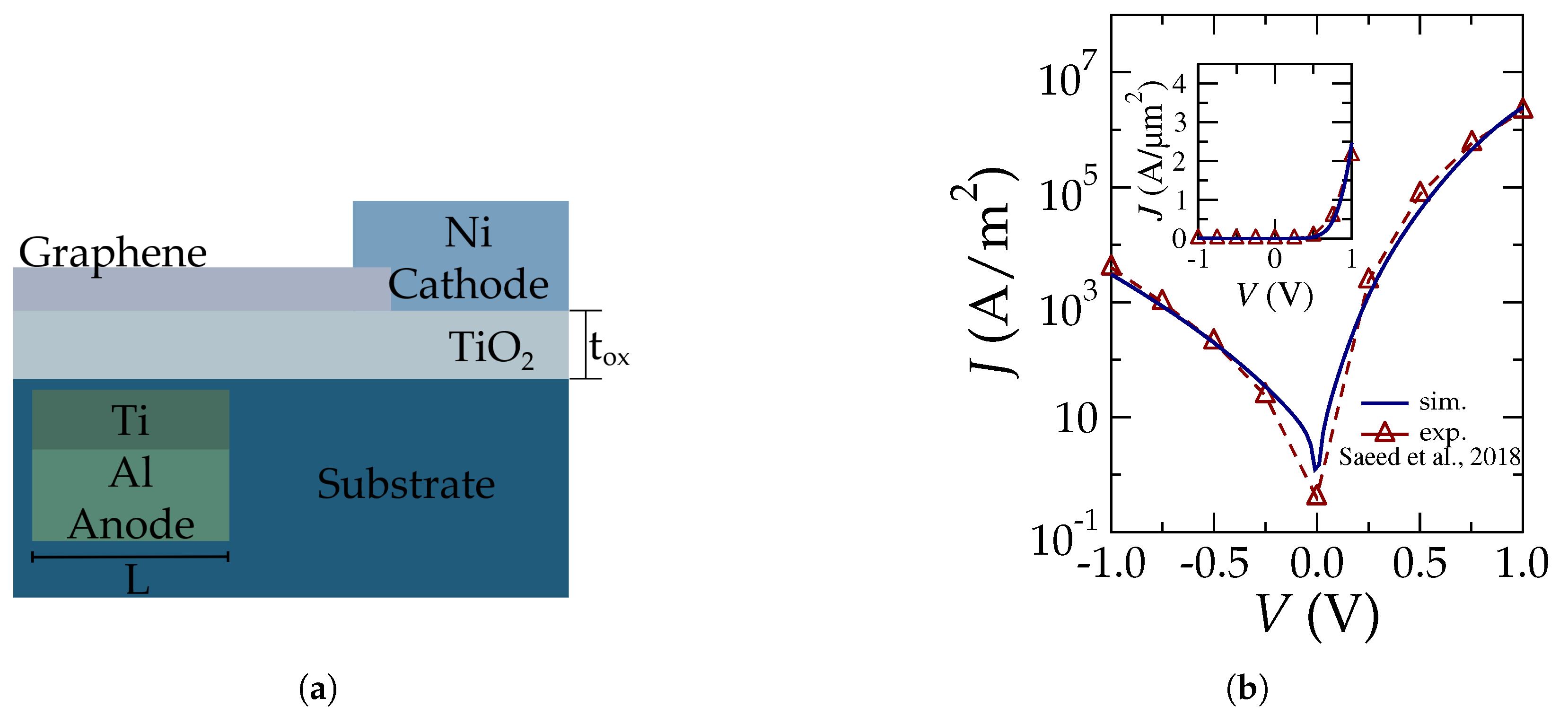
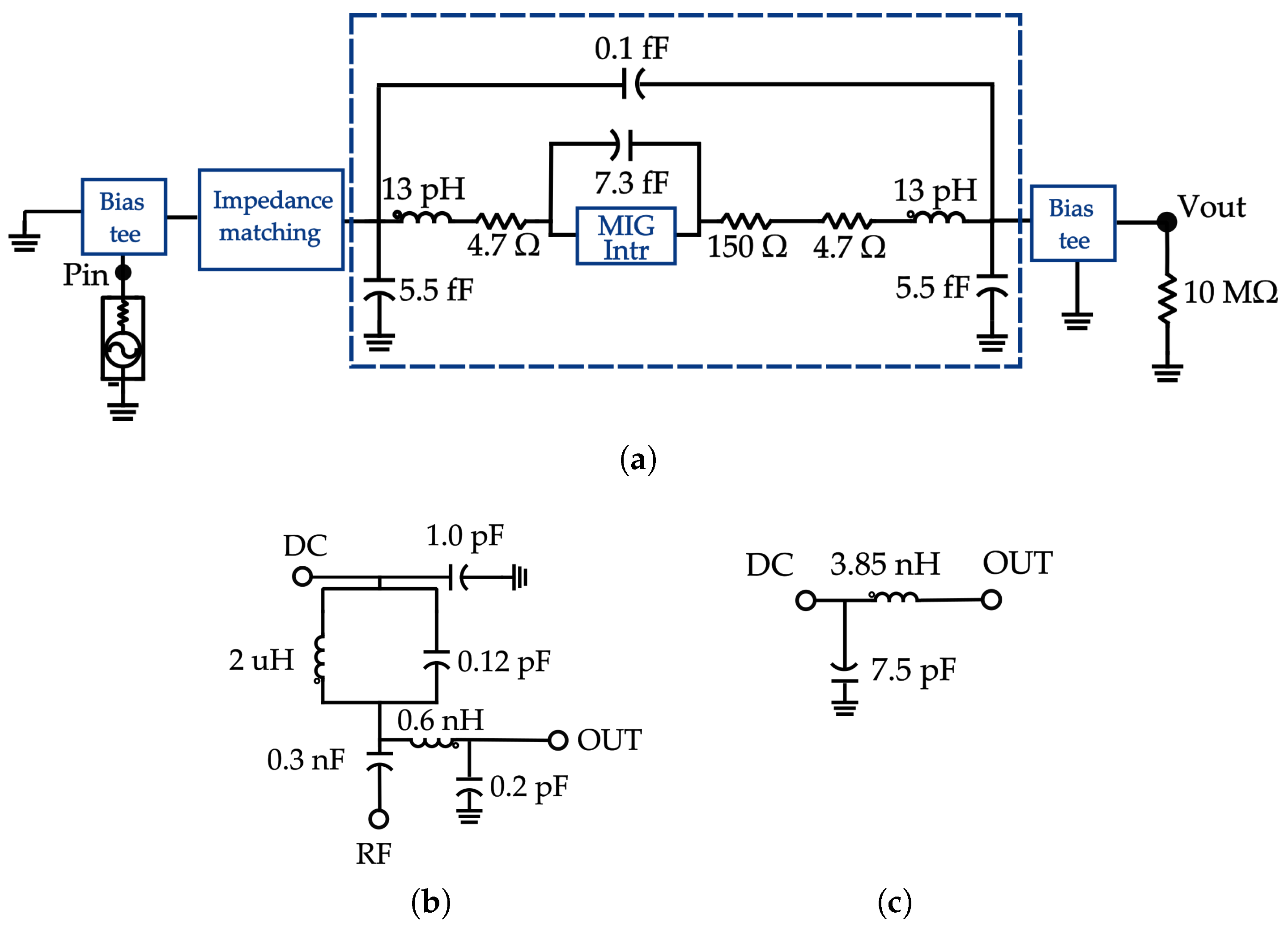
2. MIG Device and Modeling
3. Model-Based Performance Projection of MIG Rectifiers
3.1. Rectifying Metrics from DC Characteristics
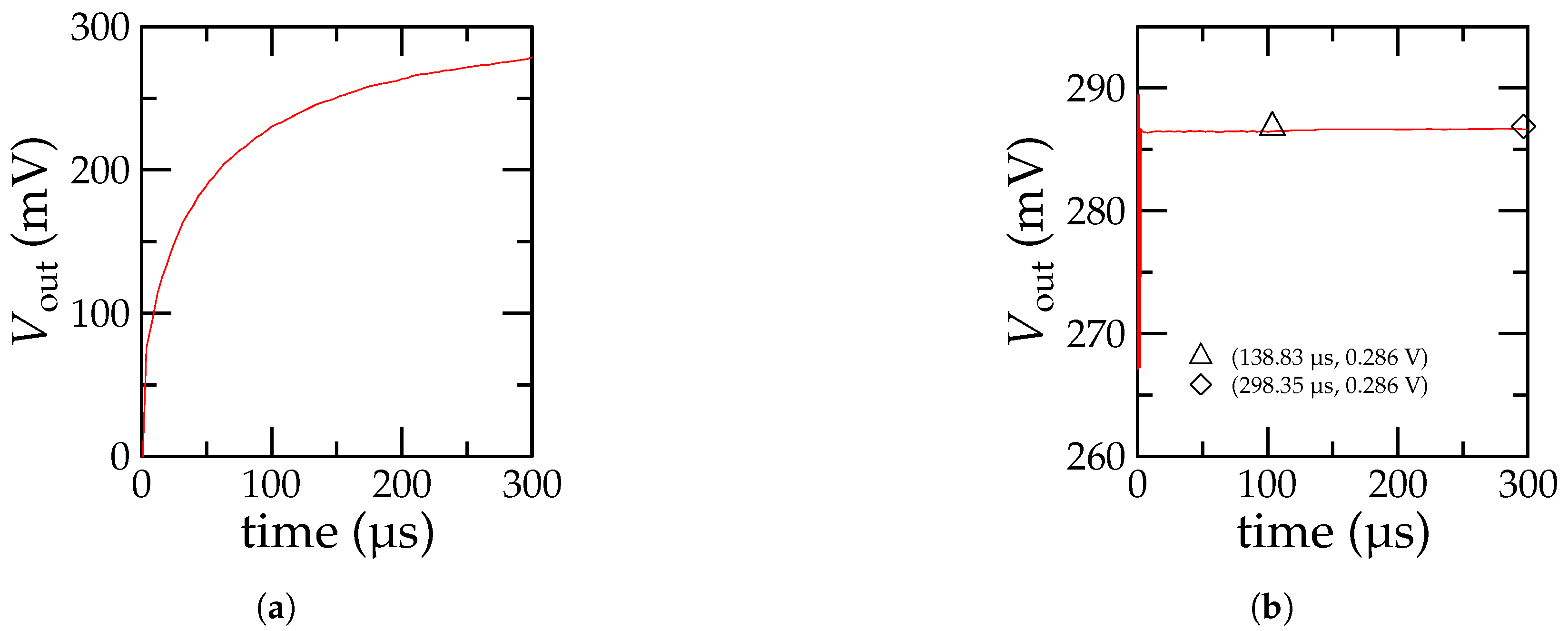
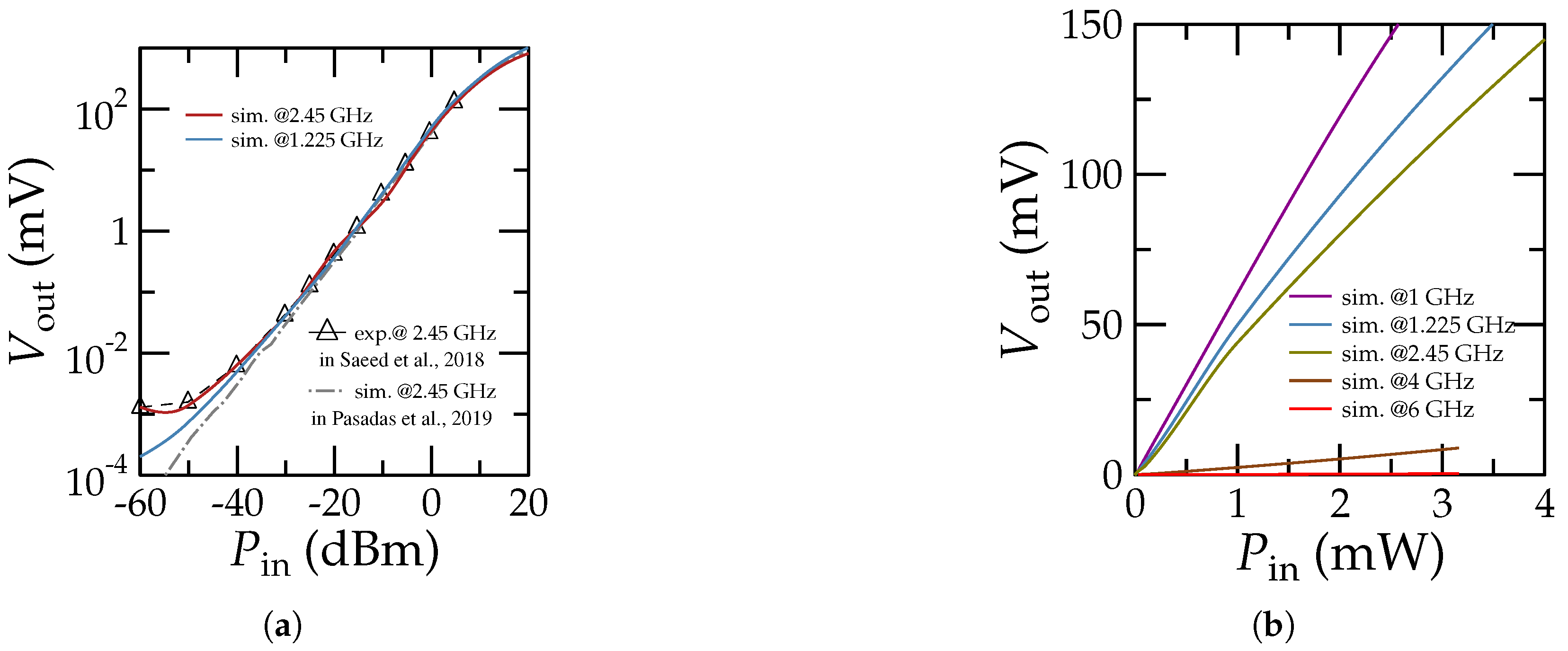
3.2. Power Detection
4. Conclusions
Author Contributions
Funding
Institutional Review Board Statement
Informed Consent Statement
Data Availability Statement
Conflicts of Interest
References
- Ghivela, G.C.; Sengupta, J. The Promise of Graphene: A Survey of Microwave Devices Based on Graphene. IEEE Microwave Mag. 2020, 21, 48–65. [Google Scholar] [CrossRef]
- Saeed, M.; Palacios, P.; Wei, M.-D.; Baskent, E.; Fan, C.-Y.; Uzlu, B.; Wang, K.-T.; Hemmetter, A.; Wang, Z.; Neumaier, D.; et al. Graphene-based microwave circuits: A review. Adv. Mater. 2022, 34, 2108473. [Google Scholar] [CrossRef] [PubMed]
- Pasadas, F.; Medina-Rull, A.; Ruiz, F.G.; Ramos-Silva, J.N.; Pacheco-Sanchez, A.; Pardo, M.C.; Toral-Lopez, A.; Godoy, A.; Ramírez-García, E.; Jiménez, D.; et al. Exploiting ambipolarity in graphene field-effect transistors for novel designs on high-frequency analog electronics. Small 2023, 19, 2303595. [Google Scholar] [CrossRef] [PubMed]
- Shaygan, M.; Wang, Z.; Elsayed, M.S.; Otto, M.; Iannaccone, G.; Ghareeb, A.H.; Fiori, G.; Negra, R.; Neumaier, D. High performance metal–insulator–graphene diodes for radio frequency power detection application. Nanoscale 2017, 9, 11944–11950. [Google Scholar] [CrossRef] [PubMed]
- Fan, C.-Y.; Wei, M.-D.; Saeed, M.; Hamed, A.; Negra, R.; Wang, Z.; Shaygan, M.; Neumaier, D. Large-signal metal–insulator–graphene diode model on a flexible substrate for microwave application. In Proceedings of the IEEE MTT-S International Conference on Numerical Electromagnetic and Multiphysics Modeling and Optimization (NEMO), Reykjavik, Iceland, 8–10 August 2018. [Google Scholar] [CrossRef]
- Wang, Z.; Uzlu, B.; Shaygan, M.; Otto, M.; Ribeiro, M.; González Marín, E.; Iannaccone, G.; Fiori, G.; Elsayed, M.S.; Negra, R.; et al. Flexible one-dimensional metal–insulator–graphene diode. ACS Appl. Electron. Mater. 2019, 1, 945–950. [Google Scholar] [CrossRef]
- Hamed, A.; Saeed, M.; Wang, Z.; Shaygan, M.; Neumaier, D.; Negra, R. Graphene-diode-based frequency conversion mixers for high-frequency applications. In Proceedings of the IEEE MTT-S International Microwave Workshop Series on Advanced Materials and Processes for RF and THz Applications (IMWS-AMP), Bochum, Germany, 16–18 July 2019. [Google Scholar] [CrossRef]
- Semple, J.; Georgiadou, D.G.; Wyatt-Moon, G.; Gelinck, G.; Anthopoulos, T.D. Flexible diodes for radio frequency (RF) electronics: A materials perspective. Semicond. Sci. Technol. 2017, 32, 123002. [Google Scholar] [CrossRef]
- Ravanne, J.G.; Then, Y.L.; Su, H.T.; Hijazin, I. Microwave power detectors in different CMOS design architectures: A review. IEEE Microw. Mag. 2022, 23, 76–84. [Google Scholar] [CrossRef]
- Zhang, T.; Eisenstadt, W.R.; Fox, R.M. A novel 5 GHz RF power detector. In Proceedings of the IEEE International Symposium on Circuits and Systems (ISCAS), Vancouver, BC, Canada, 23–26 May 2004. [Google Scholar] [CrossRef]
- Milanovic, V.; Gaitan, M.; Marshall, J.C.; Zaghloul, M.E. CMOS foundry implementation of Schottky diodes for RF detection. IEEE Trans. Electron Devices 1996, 43, 2210–2214. [Google Scholar] [CrossRef]
- Jeon, W.; Firestone, T.M.; Rodgers, J.C.; Melngailis, J. Design and fabrication of Schottky diode, on-chip RF power detector. Solid-State Electron. 2004, 48, 2089–2093. [Google Scholar] [CrossRef]
- Saeed, M.; Hamed, A.; Wang, Z.; Shaygan, M.; Neumaier, D.; Negra, R. Graphene integrated circuits: New prospects towards receiver realisation. Nanoscale 2018, 10, 93–99. [Google Scholar] [CrossRef] [PubMed]
- Saeed, M.; Hamed, A.; Negra, R.; Shaygan, M.; Wang, Z.; Neumaier, D. Zero-bias, 50 dB dynamic range, V-band power detector based on CVD graphene-on-glass. In Proceedings of the IEEE MTT-S International Microwave Symposium (IMS), Honolulu, HI, USA, 4–9 June 2017. [Google Scholar] [CrossRef]
- Saeed, M.; Palacios, P.; Wei, M.-D.; Baskent, E.; Fan, C.-Y.; Uzlu, B.; Wang, K.-T.; Hemmetter, A.; Wang, Z.; Neumaier, D.; et al. Compact V-Band MMIC Square-Law Power Detector with 70 dB Dynamic Range Exploiting State-of-the-Art Graphene Diodes. In Proceedings of the 2021 IEEE MTT-S International Microwave Symposium (IMS), Atlanta, GA, USA, 6–11 June 2021; IEEE: New York, NY, USA, 2021; pp. 888–891. [Google Scholar] [CrossRef]
- Pasadas, F.; Saeed, M.; Hamed, A.; Wang, Z.; Negra, R.; Neumaier, D.; Jiménez, D. Large-signal model of the metal–insulator–graphene diode targeting RF applications. IEEE Electron Device Lett. 2019, 40, 1005–1008. [Google Scholar] [CrossRef]
- Ang, Y.S.; Yang, H.Y.; Ang, L.K. Universal Scaling Laws in Schottky Heterostructures Based on Two-Dimensional Materials. Phys. Rev. Lett. 2018, 121, 056802. [Google Scholar] [CrossRef] [PubMed]
- Crupi, G.; Schreurs, D. (Eds.) Microwave De-Embedding: From Theory to Applications; Elsevier Science: Amsterdam, The Netherlands, 2013; ISBN 978-0-12-401700-9. [Google Scholar]
- Shaygan, M.; Otto, M.; Sagade, A.A.; Chavarin, C.A.; Bacher, G.; Mertin, W.; Neumaier, D. Low Resistive Edge Contacts to CVD-Grown Graphene Using a CMOS Compatible Metal. Ann. Phys. 2017, 529, 1600410. [Google Scholar] [CrossRef]
- Saeed, M.; Hamed, A.; Wang, Z.; Shaygan, M.; Neumaier, D.; Negra, R. Metal–insulator–graphene diode mixer based on CVD graphene-on-glass. IEEE Electron Device Lett. 2018, 39, 1104–1107. [Google Scholar] [CrossRef]
- Gahoi, A.; Kataria, S.; Driussi, F.; Venica, S.; Pandey, H.; Esseni, D.; Selmi, L.; Lemme, M.C. Dependable Contact Related Parameter Extraction in Graphene–Metal Junctions. Adv. Electron. Mater. 2020, 6, 2000386. [Google Scholar] [CrossRef]
- Cowley, A.M.; Sorensen, H.O. Quantitative comparison of solid-state microwave detectors. IEEE Trans. Microw. Theory Tech. 1966, 14, 588–602. [Google Scholar] [CrossRef]
- Agilent Technologies. Transient and Convolution Simulation. September 2011. Available online: https://edadownload.software.keysight.com/eedl/ads/2011/pdf/cktsimtrans.pdf (accessed on 15 April 2025).
- Qayyum, S.; Negra, R. Analysis and Design of Distributed Power Detectors. IEEE Trans. Microw. Theory Tech. 2018, 66, 4191–4203. [Google Scholar] [CrossRef]
- Saeed, M.; Hamed, A.; Wang, Z.; Shaygan, M.; Neumaier, D.; Negra, R. Zero-Bias 50-dB Dynamic Range Linear-in-dB V-Band Power Detector Based on CVD Graphene Diode on Glass. IEEE Trans. Microw. Theory Tech. 2018, 66, 2018–2024. [Google Scholar] [CrossRef]
- Baskent, E.; Wang, Z.; Lemme, M.C.; Negra, R. K-Band Graphene-Based Electrically Tunable Hybrid Coupler. In Proceedings of the 2024 IEEE Asia-Pacific Microwave Conference (APMC), Bali, Indonesia, 17–20 November 2024; pp. 1281–1283. [Google Scholar] [CrossRef]
- Baskent, E.; Wang, Z.; Lemme, M.C.; Negra, R. Ka-Band Metal-Insulator-Graphene Diode-Based Thin-Film Cascaded Reflective-Type Phase Shifter. In Proceedings of the 2024 19th European Microwave Integrated Circuits Conference (EuMIC), Paris, France, 23–24 September 2024; pp. 311–314. [Google Scholar] [CrossRef]
- Kunc, J.; Fridrišek, T.; Shestopalov, M.; Jo, J.; Park, K. Graphene–insulator–metal diodes: Enhanced dielectric strength of the Al2O3 barrier. AIP Adv. 2024, 14, 095207. [Google Scholar] [CrossRef]


| Ref. | * | |||
|---|---|---|---|---|
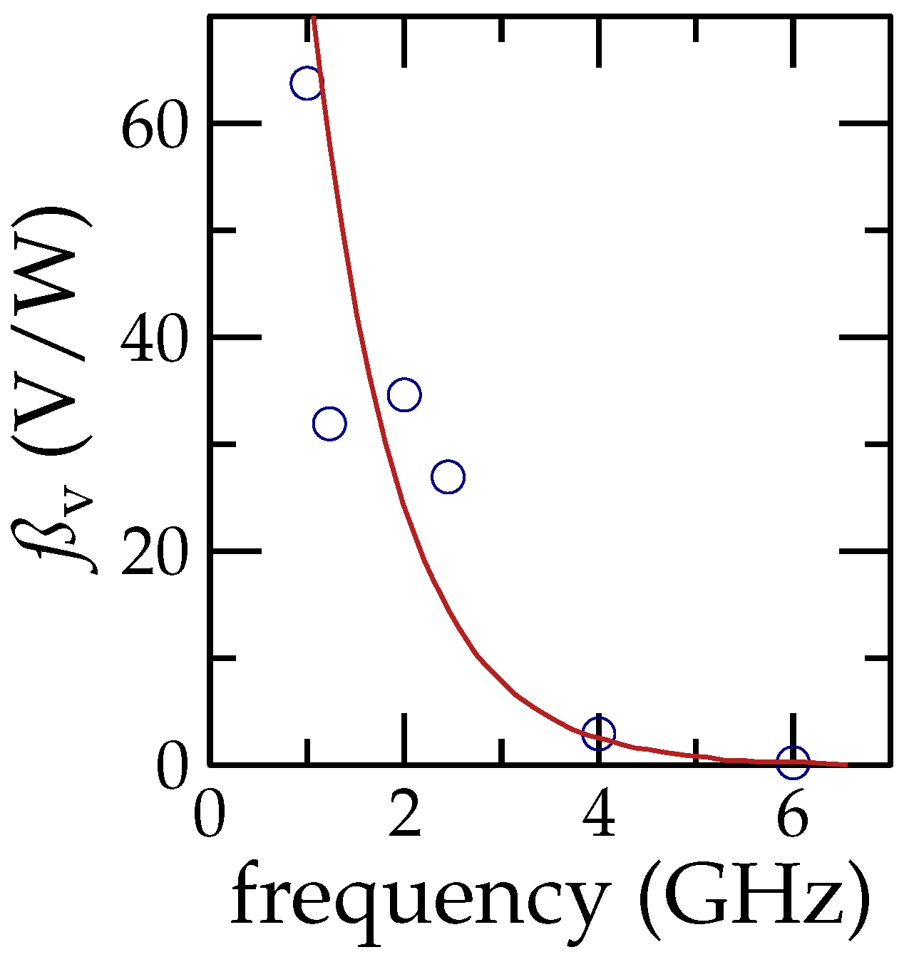
| this work | 806.6 at 1 V | 6.64 at 0.7 V | 14.65 | 63.7 V/W at 1 GHz, 31.9 V/W at 1.225 GHz, 34.6 V/W at 2 GHz, 26.9 V/W at 2.45 GHz, 2.9 V/W at 4 GHz and 0.2 V/W at 6 GHz |
| [4] | 270 at 1.1 V | 11 a 0.7 V | 12 at 0.2 V | 2.8 V/W at 2.4 GHz and 2.2 V/W at 30.8 GHz |
| [6] | 18 at 0.9 V | 3 at 0.3 V | 8 at 0.1 V | - |
| [13] | - | - | - | 42 V/W a 2.45 GHz |
| [20] | 608 | - | 10 | - |
| [16] | - | - | 12.4 | 43.6 V/W at 2.45 GHz |
| [15] | - | - | 71 | - |
| [25] | Up to 525 | Up to 10 | Up to 13.5 | 15 V/W at 60 GHz and 168 V/W at 2.5 GHz |
| [26,27] | above 400 | above 20 | - | - |
| [28] | - | - | ** 10–20 S/V | - |
Disclaimer/Publisher’s Note: The statements, opinions and data contained in all publications are solely those of the individual author(s) and contributor(s) and not of MDPI and/or the editor(s). MDPI and/or the editor(s) disclaim responsibility for any injury to people or property resulting from any ideas, methods, instructions or products referred to in the content. |
© 2025 by the authors. Licensee MDPI, Basel, Switzerland. This article is an open access article distributed under the terms and conditions of the Creative Commons Attribution (CC BY) license (https://creativecommons.org/licenses/by/4.0/).
Share and Cite
Cruz-Rodríguez, L.P.; Pardo, M.C.; Pacheco-Sanchez, A.; Ramírez-García, E.; Ruiz, F.G.; Pasadas, F. Radiofrequency Performance Analysis of Metal-Insulator-Graphene Diodes. Appl. Sci. 2025, 15, 5926. https://doi.org/10.3390/app15115926
Cruz-Rodríguez LP, Pardo MC, Pacheco-Sanchez A, Ramírez-García E, Ruiz FG, Pasadas F. Radiofrequency Performance Analysis of Metal-Insulator-Graphene Diodes. Applied Sciences. 2025; 15(11):5926. https://doi.org/10.3390/app15115926
Chicago/Turabian StyleCruz-Rodríguez, Leslie Paulina, Mari Carmen Pardo, Anibal Pacheco-Sanchez, Eloy Ramírez-García, Francisco G. Ruiz, and Francisco Pasadas. 2025. "Radiofrequency Performance Analysis of Metal-Insulator-Graphene Diodes" Applied Sciences 15, no. 11: 5926. https://doi.org/10.3390/app15115926
APA StyleCruz-Rodríguez, L. P., Pardo, M. C., Pacheco-Sanchez, A., Ramírez-García, E., Ruiz, F. G., & Pasadas, F. (2025). Radiofrequency Performance Analysis of Metal-Insulator-Graphene Diodes. Applied Sciences, 15(11), 5926. https://doi.org/10.3390/app15115926