1. Introduction
Maximum power point tracking (MPPT) is an essential part of photovoltaic (PV) systems [
1,
2,
3,
4,
5,
6]. With the increasing demand of solar PV energy, improving the performance and efficiency of the MPPT process is a necessity and a challenge at the same time [
7,
8,
9,
10,
11]. Classically, the MPPT is performed using either the inverter directly or by a DC–DC converter as a previous stage [
12,
13]. In either case, the whole amount of power passes through the converter and gets processed to achieve maximum power. The higher the size of the PV system, the higher the size of the converter, making it more challenging to maintain efficiency and compactness while processing this amount of power. However, in most PV applications, variations in solar irradiance, module degradation, or shading can cause individual modules in a string to operate at different power levels, leading to energy losses and reduced overall efficiency [
14,
15,
16]. Recently, designers have introduced a new power processing method, which is known as partial power processing (PPP) [
17,
18,
19]. In this approach, modules are connected in series and the bulk of available energy is transferred directly to the inverter. Any other mismatch is processed through a power optimizer converter. PPP-based architectures are comprised of DC–DC converters that are specially designed to only process part of the power to achieve MPPT across the entire string [
20,
21]. This gives many advantages in the design of such converters, making them smaller and more compact. The power loss of such converters is much lower, even if the efficiency of the converter is lower because only a fraction of the power is processed and the majority is transferred directly.
PPP-based architectures can be categorized into Differential Power Converters (DPCs), Partial Power Converters (PPCs), and Mixed PPP Strategies [
22,
23]. DPCs are designed to balance current mismatches between series-connected elements, such as battery cells or photovoltaic (PV) modules. Instead of processing the full power flowing from the source to the load, DPCs only handle the power imbalance between elements, significantly improving system efficiency while reducing conversion losses and thermal stress. They can be further classified into Element-to-Element (E2E) converters, which transfer power between adjacent elements, and Bus-to-Element (B2E) converters, which transfer power between an element and a common bus [
24]. E2E architectures, often implemented using Boost type [
25], buck-boost [
26], or Flyback topologies [
21], offer lower component stress and reduced switching losses but require complex control mechanisms to ensure stable operation. B2E architectures, though, offer greater modularity and higher efficiency; however, these architectures require higher voltage-rated components and suffer from increasing cost and greater complexity.
DPC control strategies are different depending on the topologies used and the systems architecture. In E2E, the control scheme focuses on redistributing power among neighboring modules (or cells), so each converter must sense and regulate the current flow only between adjacent elements. Consequently, the control is typically more decentralized, with each E2E unit operating in a cooperative manner to balance local mismatches across the chain. In [
27], each differential power processing (DPP) converter asynchronously performs local MPPT on its submodule by regulating the submodule current to match its maximum power point. Concurrently, a central (string-level) controller or inverter regulates the bus voltage by adjusting the overall string current. In [
28], each module uses a dual-loop control, with an inner voltage loop regulating its local PV module voltage and an outer power loop that runs a local MPPT algorithm to set the voltage reference. By relying solely on locally measured signals (without inter-module communication), each converter processes only the differential power needed to mitigate module mismatch, ensuring plug-and-play functionality and improved overall efficiency. In contrast, B2E differential power processing interfaces each module with a common bus, requiring the control to compare a module’s operating point against the bus voltage. This allows for more direct and centralized MPPT control on each module relative to the bus, but it also necessitates higher-voltage-rated components and a more complex converter design to accommodate the bus-based power transfers. The distributed MPP approach is more common in DPC; however, some implementations incorporate a bus interphase to minimize the local power processing units and centralize the control strategy, such as [
29]. In [
9], each PV module is first set to its maximum power point via local MPPT in the differential power processing (DPP) structure, and then the system finds the specific module whose current dictates the substring current that results in the least total processed power (LPP). By turning off that module’s DPP converter, the substring current is forced to match that module’s MPPT current, thereby minimizing the overall power processed by the remaining converters.
In this paper, a hybrid topology is presented with a unique layout, where it combines the advantages of both E2E and B2E architectures while avoiding some of their drawbacks. The following are the salient features of the proposed architecture over existing methods:
Simple Converter Topology: A simple and low-rated buck converter is employed as a power optimizer for each module, which does not utilize the magnetic coupling or high frequency transformer, hence the core losses are negligible.
Selective Converter Operation: The selective activation of buck converters ensures that shaded modules adjust their operating points to match the string current, thereby minimizing mismatch losses.
Flexible Layout: The power flow layout of the proposed architecture is such that under shading conditions, the currents of only shaded PV modules are diverted to the output side of their respective buck converters to maintain the common string current. Meanwhile, under uniform condition, a conventional series-connected string is maintained and all converters are in a dormant state.
No Extra Current from Inverter’s Node: In order to maintain a common string current, the proposed architecture does not need extra current from the DC-bus or inverter’s node, thus avoiding complex topologies, isolated components, intense coordination between converters, and a sophisticated control setup.
Simple Control: The control setup of the proposed architecture is not complex because of its simple layout and involvement of basic converters.
Low Voltage Stress: The switching devices experience low voltage stress in the proposed architecture.
Numerous simulation experiments have been performed to test the effectiveness of the proposed architecture under different shading cases, which validate the correct and high efficiency operation of the proposed converter. The comparative analysis also highlights the enhanced features of the proposed architecture over existing solutions. Thus, the proposed architecture will be a sound addition in the distributed PV energy systems.
2. Architectures Analysis
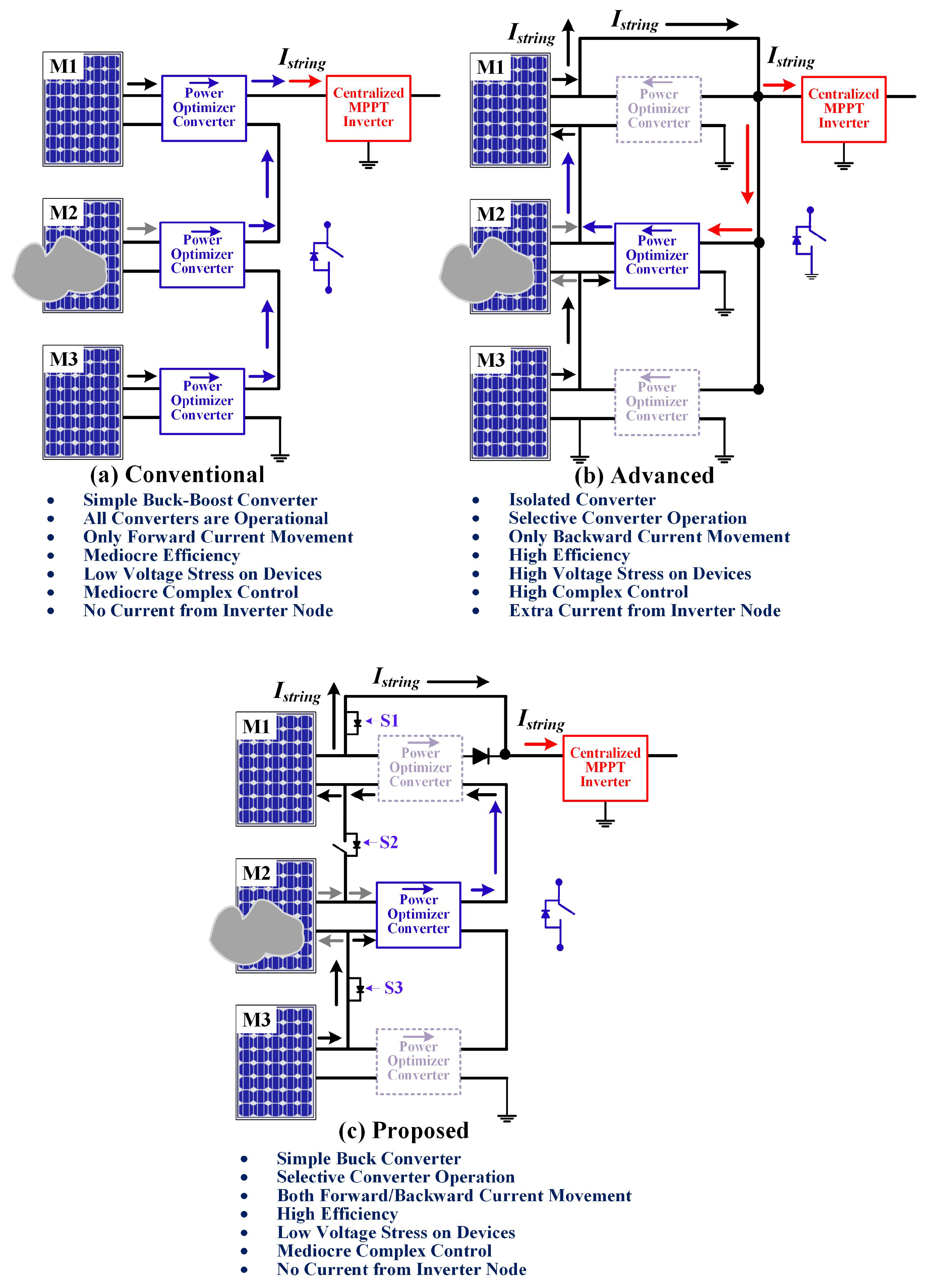
The main focus of this paper is to design a power optimizer architecture for PV string, which is interfaced with a centralized MPPT inverter. Three architectures, conventional, advanced, and proposed, are presented in
Figure 1, where MPPT operation of the string is managed by a centralized inverter. Note that in such architectures, each DC–DC converter at module-level serves as a unit-level power optimizer to ensure that it maintains the common string current (
) under adverse mismatch effects, such as partial shading. The discussion about the operation and features of the architectures are as follows.
Figure 1a displays the conventional architecture, in which a buck-boost converter is usually used for each module. In this architecture, each module-level converter is always active, and the common string current (
) is maintained at the output ports of converters. For instance, the lower current generation of module M2, due to partial shading, is mitigated at the output port of the converter, where the converter is set in buck-mode and duty cycle (
D) is adjusted to make the output current equivalent to the string current. Other modules may operate at low
D values. This architecture lacks the ability of a selective converter operation, which, in turn, reduces its efficiency, as the operations of all converters increase the power processing loss. However, the voltage stress on switching devices is lower, as the converters do not make the parallel connection with an inverter, meaning this architecture does not need to draw extra current from the inverter’s DC-link node. Besides, the control operation is relatively simple since basic topology is used for each converter.
Figure 1b shows the advanced architecture, in which each module-level converter is designed through an isolated topology [
21]. In this architecture, all the modules are connected in series and common
is maintained at the PV modules side by providing extra current from the inverter DC-link node. For that, only isolated converters of shaded modules are made active. For instance, the low current at the node of shaded module M2 is lifted through its isolated converter, which takes an extra differential current from the inverter node and supplies it to the M2 node to support the
. Simultaneously, the converters of modules M1 and M2 are dormant. Because of the selective operation of converters, the efficiency of the architecture is good. However, the complexity of the system is high because of the involvement of magnetic components in each converter. Another issue is the higher stress on switching devices, as all the converters make the parallel connection with the inverter’s DC-link node. Moreover, the control complexity of the system is high. Another important aspect is that if all converters are operational, the overall efficiency of this architecture becomes even lower than the basic architecture because isolated converters operate with higher power processing losses.
3. Proposed Design and System-Level Development
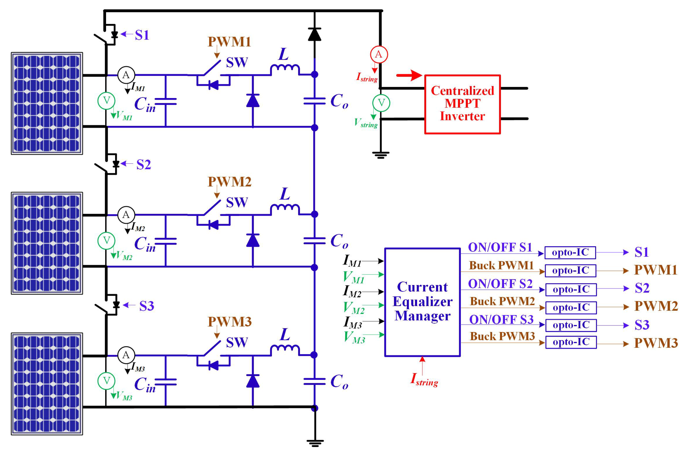
Figure 1c presents the proposed architecture, in which a buck converter is used for each module as a power optimizer. The schematic diagram of the architecture is shown in
Figure 2. A unique feature is that all PV modules are connected in series through string switches, and simultaneously, the output ports of all the buck converters are also connected in series. It means that in order to maintain
, the string switch of a specific module is made active if it supports the
, otherwise the module’s current is diverted to the output port of the buck converter. Since the buck converter enhances the output current, it becomes possible to raise the module’s current to
at the output port of the converter.
The buck converter is a basic topology, which steps down the voltage at its output. The output voltage and output current relations of the buck converter in continuous conduction mode are expressed in Equations (
1) and (
2), respectively, when the PV module is interfaced with the converter. Here,
D represents the duty cycle of the converter. As is well known, partial shading impacts the power generation of the PV source [
30]. In general, the
of the PV module reduces, and its
rises during a partial shading condition, which makes the buck converter an ideal candidate for the proposed architecture to enhance the shaded module’s current at the output of the buck converter in order to match the common string current.
Figure 1c shows that the string switch of only M2 is turned off, and its corresponding buck converter is made active to support the
, while the string switches of M1 and M3 remain active, as they can support the
. Clearly, the proposed architecture uses both forward (towards the converter’s output port) and backward (towards the module side) current movements to maintain the
. Because of this philosophy, the selective operation of converters become possible, thus making the architecture’s efficiency high. Simultaneously, since extra current is not needed from the DC-link node, the stress on switching devices is lower. The control operation is not complex, as buck converters and simple On/Off control of string switches are involved. It should be noted that the centralized MPPT inverter ensures the MPP operation of the string.
3.1. Schematic of Proposed Architecture
Figure 2 shows the schematic diagram of the proposed architecture, which contains three PV modules. All PV modules are connected in series through string switches, which are controlled in an On/Off manner to control the flow of the common string current (
). Each PV module is equipped with a buck converter, where the switches of all these converters are controlled by pulse width modulation (PWM) pulses. Note that On/Off signals for all string switches and PWM pulses for all buck converters are controlled by a current equalizer manager. This manager block takes the current, voltage values of each module, and
value through sensors. Based on this information, the current equalizer manager applies its control mechanism, the details of which are explained in the upcoming section.
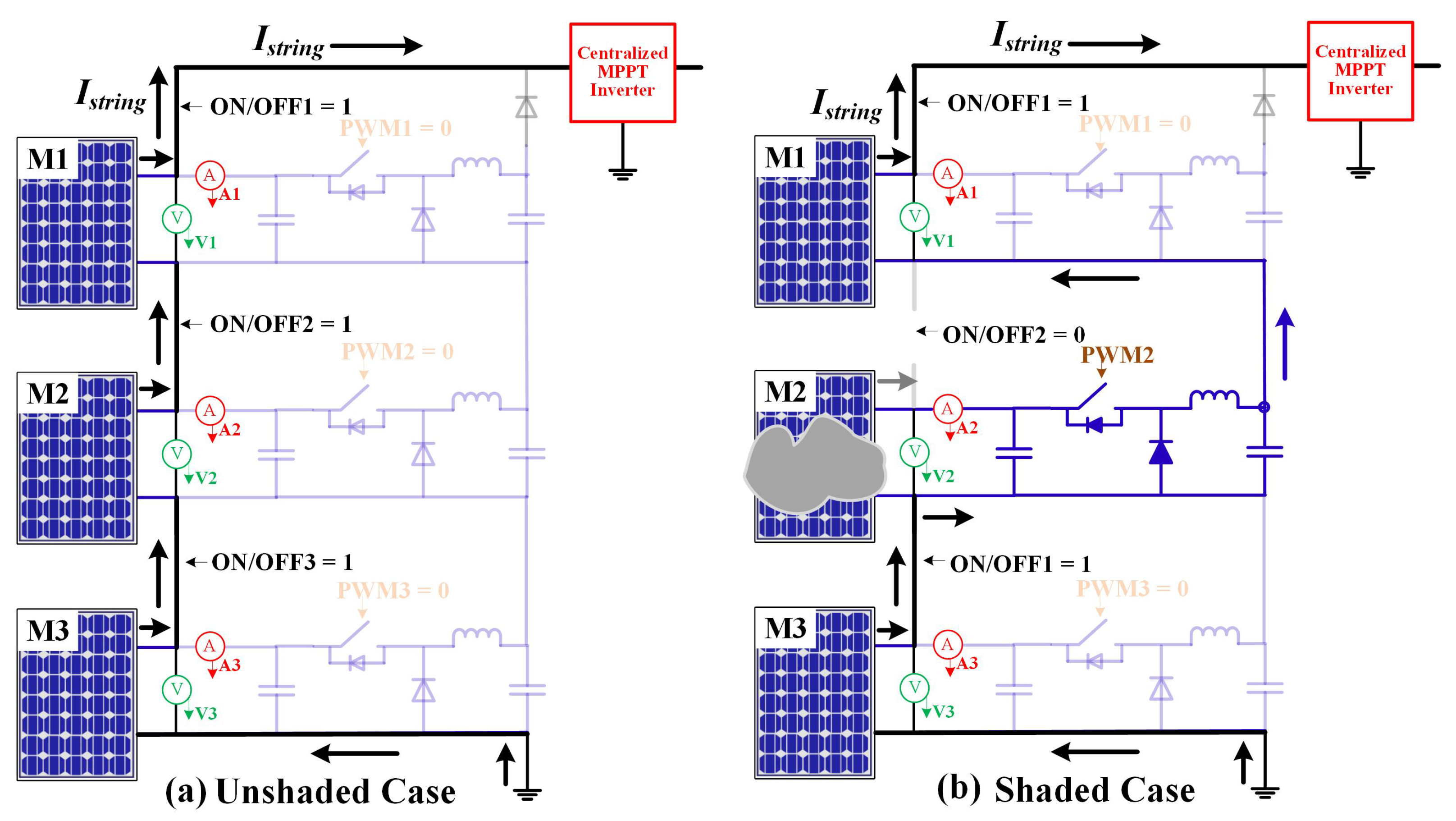
3.2. Operation Under Uniform Condition
Figure 3a shows the flow of
through the proposed architecture, when all PV modules are under uniform condition. It can be seen that all the modules make a series connection through string switches, and no converter is operational. The string is directly interfaced with a centralized MPPT inverter, which ensures the maximum power point (MPP) operation of the string.
3.3. Operation Under Shading Condition
Figure 3b shows the flow of string current when M2 is under the influence of partial shading, while M1 and M3 are under the same condition. Again, the centralized MPPT inverter maintains the MPP operation. It can be seen from
Figure 3b that the maximum power point current (
) of M3 enters into the M2 node through a string switch. Since M2 does not generate the same
of M3 due to the shading condition, the string switch of M2 is switched off and the buck converter of the M2 module is made operational. It means that the
of M3 is diverted to the output port of the buck converter. Now, the duty cycle (
D) of the buck converter is adjusted appropriately to ensure that the low input current of M2 is raised to
of M3 at the output port of the converter. Simultaneously, module M2 operates at its local MPP point. Then, the
(=
) from the output port of M2’s buck converter is diverted back to the PV side, as M1 can support the
. Finally, after passing through M1, the common
(=
) reaches the inverter node.
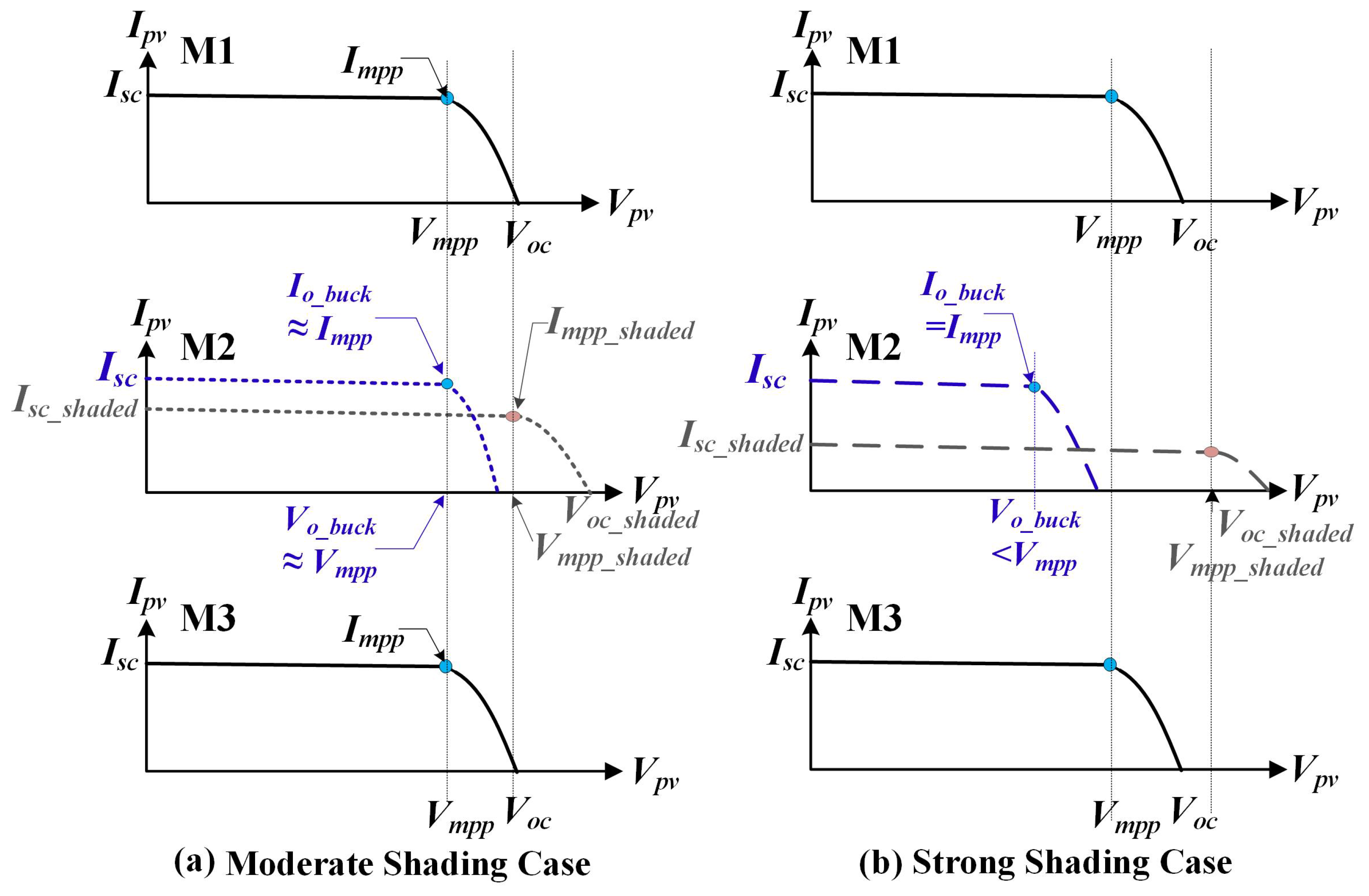
3.4. Moderate Shading, I-V Characteristics, and Natural Alignment of Buck Converter
Figure 4a shows the I-V characteristics of three PV modules, where only M2 is under the influence of a moderate shading condition. Due to this,
of M2 reduces while its
increases, as shown in the light-black dotted line in
Figure 4a. This almost shifts the MPP of M2 towards the right, i.e., an increase in
as compared to other modules. Since the buck converter of only this module is active, this eventually increases the output current and reduces the output voltage, while M2 operates at its local shading MPP point. This makes the likelihood that with a moderate duty cycle operation, the output voltage and output current of the buck converter becomes equal to
and
of other M1 and M3 modules, respectively, as shown in
Figure 4a. In this manner, the basic buck converter is a natural topology to mitigate the difference in I-V characteristics of modules, which not only supports the common
, but also adjusts the voltage of shaded modules equivalent to
of other modules at its output. Because of this, the centralized inverter does not need to make a sizable difference in its DC-link voltage to track the MPP of the string.
3.5. Strong Shading, I-V Characteristics, and Buck Converter Role
Figure 4b shows the I-V characteristics of M2 when it is under the influence of an strong shading condition. In this case, the buck converter of M2 may operate at a high
D value to match the common
(=
) of string. Because
is less than the
of M1 and M3 modules, i.e., the overall voltage of string will be less. Nevertheless, the centralized MPPT inverter usually has enough room to adjust the string voltage. Note that even with strong shading conditions, there is still some probability that
of M2’s buck converter is in close proximity to the
of other modules.
4. Control Operation and Flowchart
The control diagram of the current equalizer manager is presented in
Figure 5, which can be further linked to the same block in
Figure 2, to visualize the entire control system of the proposed architecture. As already explained, in this system, the centralized MPPT inverter is responsible for performing MPP tracking of the string by adjusting its input operating point at the DC-link and thereby maximizing the overall power output.
Figure 5 indicates that the equalizer manager contains two blocks—one is the current equalizer algorithm and the other is a current matching controller. It can be seen that the current and voltage information of each module are given to the current equalizer algorithm block. Then, this block, through its algorithm, which is explained later, generates the corresponding binary On/Off signal for the string switch ‘Sn’ of each module. The switch signal is then multiplied by
after inversion to form the module’s target current reference (
) for the controller block. Note that for shaded modules, the binary signal for the string switch will be ‘0’, i.e., OFF; it means that the path of the common
will be diverted to the output of the buck converter. Further, the signal of the string switch becomes ‘1’ after inversion, which is multiplied by
to set the reference signal. On the other hand, for unshaded modules, the binary signal for the string switches will be ‘1’, and the target
is ‘0’, i.e., no PWM pulses.
The main task of the current matching controller is to make the output current of the shaded module’s buck converter equivalent to
(≈
). Here, the output current is estimated through
/
by using the shaded modules’s current
and duty cycle
of its converter. Through this feedback system, the current matching controller generates the PWM pulses of the corresponding buck converter, unless the error becomes equal to zero, as shown in
Figure 5. For this purpose, it utilizes the proportional–integral (PI) controller for PWM pulses to ensure the fast response of the system. In this manner, the buck converter of shaded modules supports the common string current.
Figure 6 shows the working flowchart of the current equalizer algorithm, where it collects each module’s current–voltage measurements (
,
,.….,
,
). The algorithm continuously monitors the power output of each PV module and compares it against a reference power (
), which is derived from the median of all modules’ power. Each module’s power is then checked to see if it falls below a certain fraction (
×
) of that reference
, where the factor
falls in the range 0.8–0.9. Modules flagged as under-performing are temporarily isolated from the string by making their respective string switch signals as ’0’, and their respective currents are raised to
through a local (MPP) buck converter, as already explained. Meanwhile, modules that are meeting or exceeding the threshold continue normal operation. This process repeats in cycles, ensuring that any mismatched or shaded modules are detected in real time and contribute to maintaining the optimal performance of the overall system.
5. Simulation Experiments, Verification, and Comparative Analysis
For the proof of concept and performance validation, the proposed architecture, as presented in
Figure 2, is modeled in a power simulation (PSIM) software to conduct simulation experiments. PSIM is a specialized simulation software for power electronics and renewable energy systems. From the built-in power source library of PSIM, the photovoltaic module is selected and is configured with the following specifications under the standard testing condition (STC):
= 6.5 A,
= 6 A,
= 21.7 V, and
= 17.2 V. A PV string is made through three series-connected PV modules, where a buck converter is used for each module. The switching frequency (
) of each converter is set at 50 kHz, while the values of the inductor (
L) and output capacitor (
) are designed at 117 μH and 1000 μF, respectively. To generate PWM pulses at the appropriate
D value for each converter and On/Off control of the string switches, the control equalizer manager and its algorithm are programmed in the C block of the PSIM software (Version 9.0). The control mechanism of the equalizer manager has already been explained in the previous section.
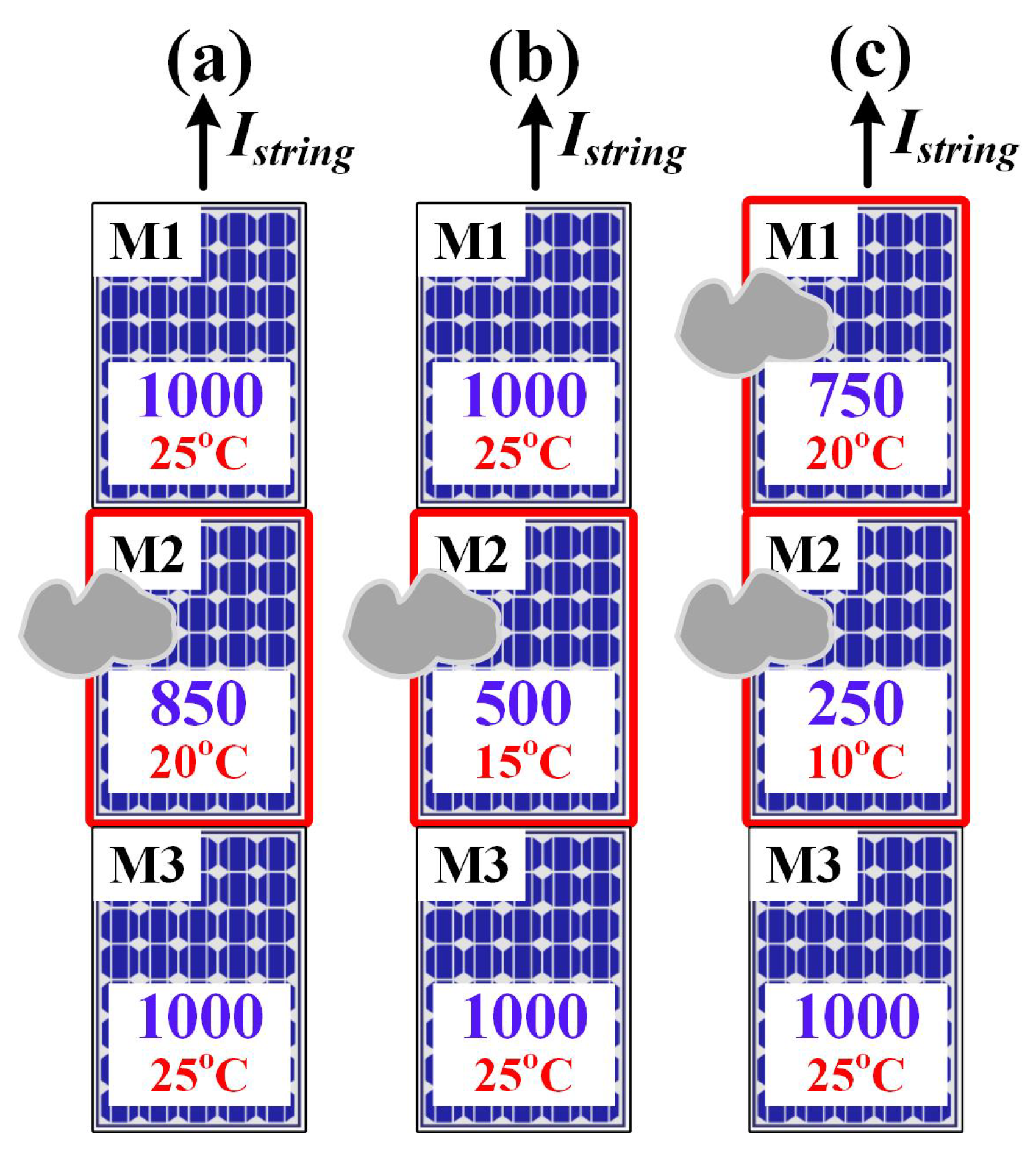
Figure 7 displays three shading cases of the PV string, which are simulated in PSIM software to assess the behavior of the proposed architecture.
Figure 7a represents the moderate shading case (MS-case), where M2 receives the irradiance of 850 W/m
2 at 20 °C, while other modules M1 and M3 receive STC. On the other hand,
Figure 7b represents the strong shading case (SS-case) as M2 receives a half irradiance value of 500 W/m
2 at 15 °C, as compared to the STC of modules M1 and M3. In response to these two shading cases, i.e., the MS-case and SS-case, the behavior of the proposed architecture is presented in
Figure 8 and
Figure 9, respectively.
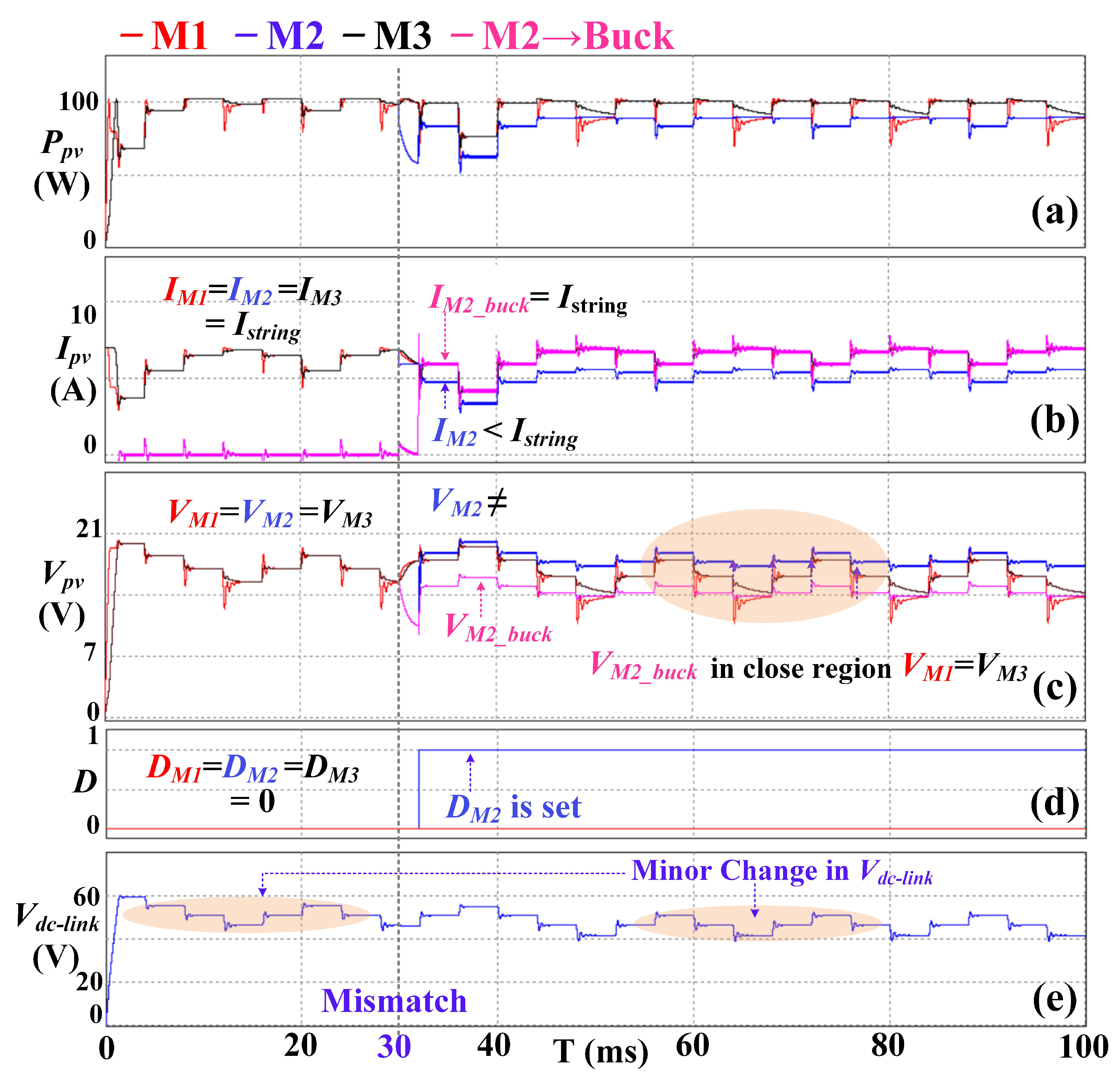
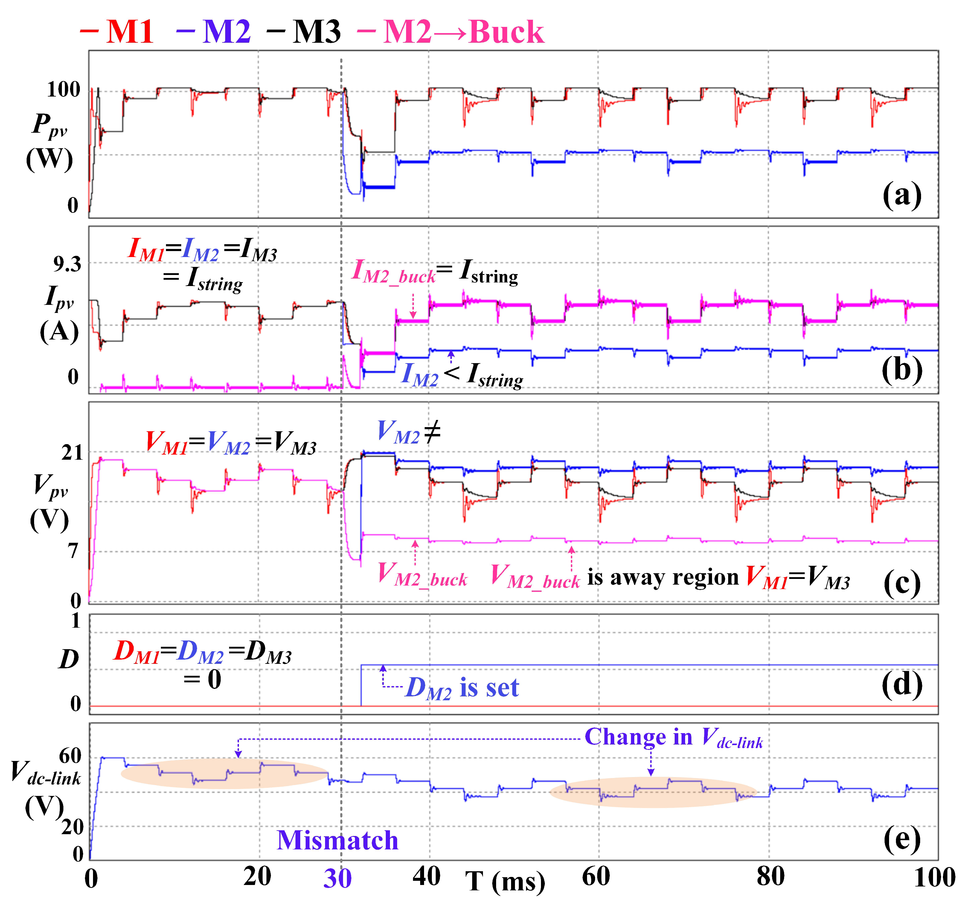
Five graphs are involved in each figure, where red, blue, and black curves of each graph represent modules M1, M2, and M3, respectively. Note that since the buck converter of only M2 becomes active because of different weather conditions, the output curves of M2’s converter are shown in a pink color. For clarity and better understanding, the features and operation of the proposed architecture are explained for both cases together:
Figure 8 shows that, initially, all modules receive the STC before 30 ms. Consequently, power (
) curves of all modules exhibit similar behavior with steady-state oscillations, as shown in
Figure 8a. These oscillations occur because of the centralized inverter, which operates with the perturb and observe algorithm for MPP tracking. In this connection, the voltage tracking steps of the inverter can be observed at the DC-link voltage (
), as shown in
Figure 8e, where the
of all modules are added, i.e., string voltage. The current (
) and voltage (
) curves of the three modules display similar characteristics, as shown in
Figure 8b,c, respectively.
Figure 8d shows that during this interval, the
D value of all converters is ’0’, which implies that all PV modules are in series and the common
flows through the modules to reach the inverter. For an interval up to 30 ms,
Figure 9 also displays the same behavior, as partial shading has not occurred yet.
At 30 ms,
Figure 8 and
Figure 9 represent the the MS-case and SS-case, respectively. It can be noticed in the graphs of both
Figure 8b and
Figure 9b that
of M2 becomes lower than
, as module M2 is under the influence of partial shading. After sensing this, the centralized current manager turns off the upper switch of module M2 and activates its buck converter by delivering the PWM pulses at an appropriate
D value. It can be confirmed from
Figure 8b and
Figure 9b that the output
current of the buck converter becomes equal to
, and M2 operates at its local MPP as well. It implies that the overall architecture takes the form as shown in
Figure 3b.
An important point can be noted from the
curves that in the moderate shading case, i.e., the MS-case in
Figure 8b, the mismatch between
and
is lower compared to the strong shading case, i.e., the SS-case in
Figure 9b. As a result, the controller sets the higher
D and lower
D values for the MS-case and SS-case, respectively, as can be seen from the graphs of both
Figure 8d and
Figure 9d. Naturally, the
curve of the MS-case is in close proximity to the
and
voltage curves of modules M1 and M3, respectively, as shown in
Figure 8c. Because of this, the inverter makes only a minor adjustment in its DC-link voltage, as indicated in
Figure 8e. In contrast, the
curve of the SS-case is at quite an offset from the
and
voltage curves of modules M1 and M3, respectively, as illustrated in
Figure 9c. Naturally, the buck converter operates at quite a different
D value to bridge the gap. Therefore, the inverter also makes more adjustments in its DC-link voltage, as shown in
Figure 9e.
These two simulation results, i.e.,
Figure 8 and
Figure 9, depict excellent resemblance to the theoretical study that is presented in
Figure 4a,b, respectively. Importantly, these results clearly highlight the correct and efficient operation of the proposed architecture.
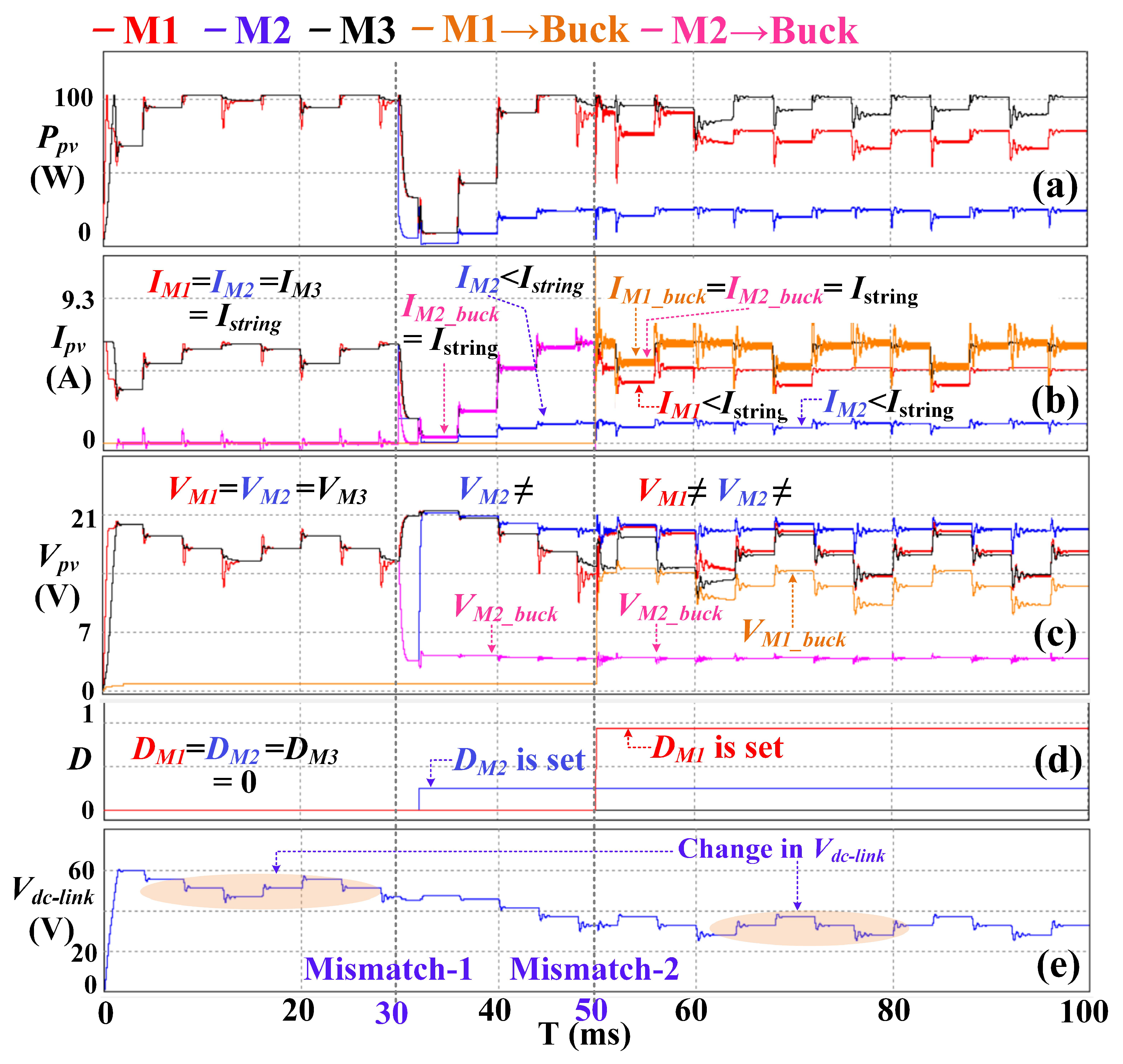
Figure 10 displays the response of the proposed architecture when two modules (M1 and M2) of PV string are under the influence of partial shading, i.e., the extreme shading case, as shown in
Figure 7c. The timeline is set as follows: (1) from 0 to 30 ms, all modules are under STC; (2) from 30 ms to 50 ms, only M2 is under the influence of 250 W/m
2–10 °C; and (3) from 50 ms onward, M1 and M2 are under the influence of 750 W/m
2–15 °C and 250 W/m
2–10 °C, respectively.
Figure 10d shows that the current equalizer manager of the proposed architecture activates the duty cycle operation of the buck converters of M2 and M1 one-by-one after 30 ms and 50 ms, respectively. The
D values are different as M2 and M1 are under different shading conditions. It can be confirmed from
Figure 10b that even under this extreme shading case, the proposed architecture manages to make the output current of M2 (pink color) and output current of M1 (brown color) of the buck converters equivalent to
. However, because of extreme shading, the centralized inverter makes a considerable adjustment in
voltage as shown in
Figure 10e.
The proposed architecture contains a converter for each module. The appropriate fabrication and operational management of each converter in terms of its thermal management, devices operation, and high efficiency are critical. Additionally, for large-scale PV plants, the effective management of multiple converters also poses a sizable challenge. Finally, the advanced control schemes can be utilized for the optimized control of converters [
31].
The proposed architecture is verified through detailed simulation experiments. Nevertheless, the authors intend to develop a small-scale prototype to experimentally validate the proposed architecture in the future.
Comparative Analysis
The comparative analysis between the three architectures, which is shown in
Figure 1, has been presented in
Table 1 and
Table 2. The first table shows the efficiencies of the architectures under three scenarios, which are based on a number of active converters. It can be confirmed from
Table 1 that the proposed architecture always maintains high efficiency (≥90%) as compared to the other two architectures. It is because of two reasons: (1) it activates the converters of only those modules that are under the influence of partial shading, and (2) it employs the basic buck topology for each module.
Table 2 describes the comparison of three architectures in the context of their respective features and other engineering aspects. The table indicates that apart from higher efficiency, the proposed architecture operates with low control complexity and its switching devices do not suffer from high voltage stress. Clearly, the proposed architectures exhibit better engineering features as compared to other architectures.
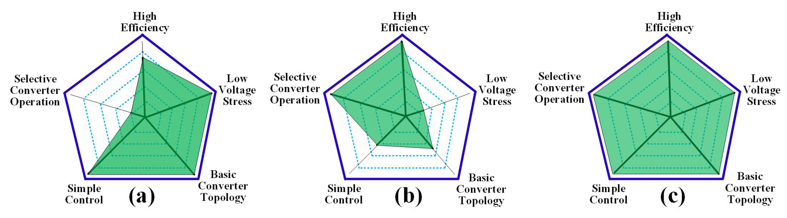
Figure 11 shows the penta-modeling graph of three architectures, which is based on five parameters. It can be seen that the horizon of the proposed architecture is quite spread as compared to other architectures.
6. Conclusions
An improved power optimizer architecture for photovoltaic (PV) string have been introduced to address partial shading, where a buck converter has been used for each module. The buck converter, typically underutilized, is shown to be well-suited for handling partial shading effects by converting the lower current from shaded modules into higher output current. The unique design philosophy, layout formation under different conditions, control mechanism, and fundamental operation of the proposed architecture have been comprehensively explained. In connection, it is proved that the proposed architecture activates only the converters for the shaded modules, without drawing additional current from the inverter’s DC-link. Because of this, the proposed architecture contains the advantages of both complex and basic architectures, i.e., offering high efficiency, low voltage stress, selective operation of basic topology, and reduced control complexity, while avoiding their respective drawbacks. The design philosophy and operation of the proposed architecture have been validated through simulations, demonstrating an efficiency exceeding 97% under normal conditions. A comparative analysis of different architectures highlights the superior performance and better features of the proposed architecture.


