Article

Sizing the Split DC Link Capacitance in Three-Phase Three-Level Bidirectional AC-DC Converters Operating with Arbitrary Power Factor Under Zero-Sequence Injection Restriction

1
Applied Energy Laboratory, School of Electrical and Computer Engineering, Ben-Gurion University of the Negev, Beer-Sheva 8410501, Israel
2
Department of Electrical Engineering and Electronics, Ariel University of Samaria, Ariel 40700, Israel
*
Author to whom correspondence should be addressed.
Appl. Sci. 2025, 15(6), 3159; https://doi.org/10.3390/app15063159
Submission received: 20 February 2025 / Revised: 4 March 2025 / Accepted: 12 March 2025 / Published: 14 March 2025
(This article belongs to the Special Issue Energy and Power Systems: Control and Management)

Abstract

:
The paper presents a methodology for determining the minimum split DC link capacitance for a family of three-phase, three-level grid-connected bidirectional AC-DC converters operating under arbitrary power factor under restriction of DC-only zero-sequence injection. The approach is based on the recently revealed generalized behavior of split DC link voltages in the above-mentioned converters family while distinguishing between leading and lagging power factors in order to highlight different impacts on split DC link capacitor voltages pulsating components. The minimum capacitance value is derived from the boundary condition, ensuring the mains voltage remains below or equal to the capacitor voltage at all times. It is revealed that operation with the lowest expected leading power factor should be employed as the design operating point. The accuracy of the proposed methodology is validated by simulations and experiments carried out employing a 10 kVA grid-connected T-type converter prototype. The results demonstrate close agreement between theoretical predictions and experiments, confirming the practical applicability of the proposed method.

1. Introduction

The ever-growing demand for high-power on/off-grid bidirectional AC-DC converters underscores their pivotal role in modern power and energy systems. As a result, multi-level converters have emerged as a preferred choice across various applications, owing to their superior performance characteristics [1]. These converters offer notable advantages such as enhanced efficiency, reduced dv/dt stress, and lower output voltage total harmonic distortion, making them indispensable in meeting stringent grid standards [2]. In addition, these converters are often required to operate with non-unity power factors, either to supply (absorb) reactive power to (from) the grid or accommodate loads operating with varying power factor [3]. Multi-level converters are known to be crucial in dual-stage power conversion systems that utilize an intermediate DC voltage link [4,5,6,7,8,9]. In such multi-level conversion systems, the DC link is usually implemented using multiple split capacitors [10,11]. The topology allows power decoupling between conversion stages and permits self-governing converter operation while employing diverse pulse width modulation (PWM) techniques [12,13,14,15,16,17,18]. In fact, 10–100 kVA rated multilevel AC-DC and DC-AC converters have become increasingly prominent across diverse industrial applications [19].
Dual-stage AC-DC and DC-AC converters usually include a short-term energy storage unit (typically realized by a capacitor bank) on the DC side to manage pulsating power components [20], maintain stable operation during power mismatches occurring during transients [21], and comply with hold-up requirements [22]. On the other hand, the capacitance of the DC link is a bottleneck in terms of physical size and reliability [23,24,25]. The DC link capacitance value is typically imposed by the hold-up time constraint. In applications where temporary loss-of-mains is tolerable, hold-up time constraint is absent, and it is possible to reduce the value of required DC link capacitance. Numerous approaches for DC link capacitance reduction have been suggested in the literature, e.g., active capacitance reduction [26,27,28], AC-side current distortion (up to minimum allowed power quality merit) [29,30], permitting DC link voltage ripple increase [31,32], etc. Minimum attainable values of DC link capacitance under active power decoupling, AC-side current distortion, notch-based DC link voltage control, and increased DC link voltage ripple were derived in [32,33,34], respectively.
A methodology for establishing a baseline for determining split DC link voltages behavior for a family of three-level, three-phase AC-DC and DC-AC power converters was revealed in [35]. The approach is based on the assumption of the third-harmonic-dominated nature of split DC link voltages ripple. The revealed approach focused on converters operating with a unity power factor and a constrained-to-DC zero-sequence component. A subsequent study [36] utilized the outcomes of [35] to derive the lowest feasible values of split DC link capacitance for the above-mentioned family of converters. The impact of operation with arbitrary power factor on the behavior of split DC link voltages was recently explored in [37]. It was shown that operation under non-unity power factor gives rise to significant high-order harmonic content, which aggregates split DC link voltage ripple magnitudes and displaces them relative to mains voltages. Consequently, the assumption of third-harmonic-only content (shown to be accurate in case of unity power factor operation in [35]) does not hold anymore. As a result, the derivation of corresponding analytical expressions is nearly unmanageable. In order to tackle this gap, a numerical solution was adopted in [37] for the derivation of a general expression for normalized split DC link ripple energy and the angle between split DC link voltages and AC-side voltages as a function of the power factor.
This work proposes a methodology for determining the minimum split DC link capacitance for the above-mentioned family of converters by utilizing the assessment of split DC link voltage behavior carried out in [37]. It is revealed that the operating point corresponding to the minimum expected leading power factor should be employed for capacitance sizing. Experimental results fully support the proposed design methodology.

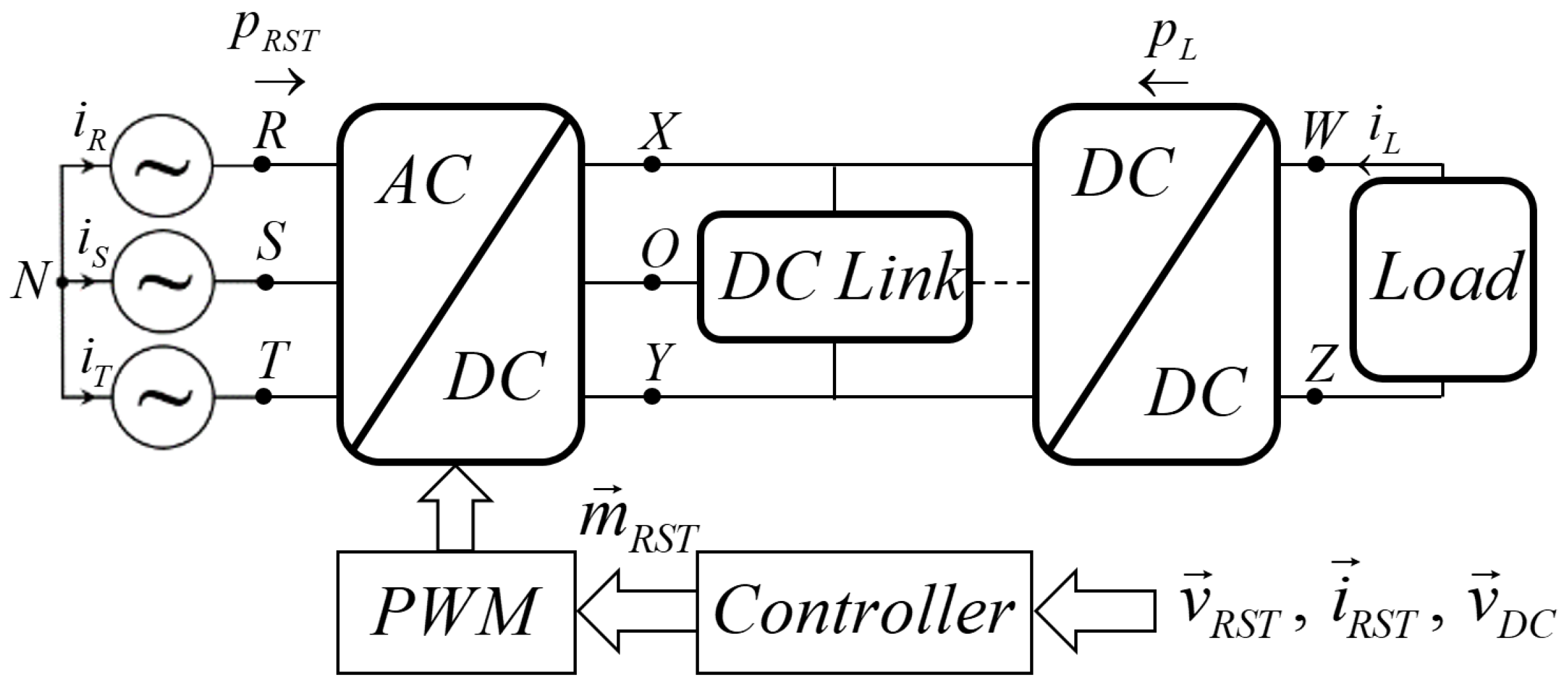
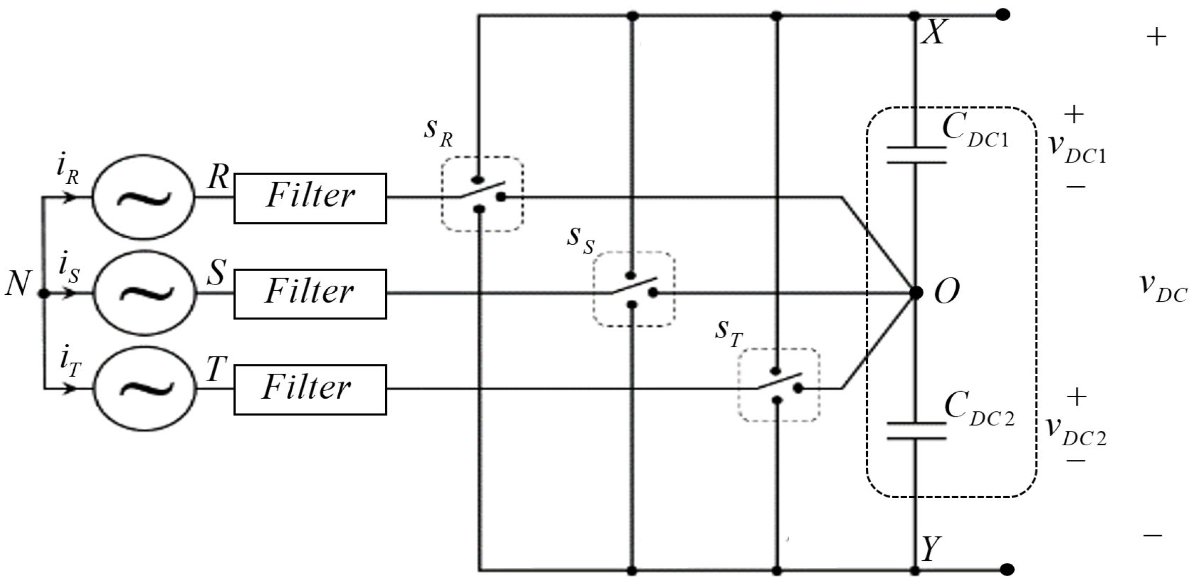
2. Split DC Link Voltages in Zero-Sequence-Restricted Three-Phase Three-Level AC-DC Converter

A common dual-stage three-phase power conversion system, consisting of a three-level AC-DC (or DC/AC) converter, a DC link, and a DC-DC converter, is depicted in Figure 1. System power flow is bidirectional in general, i.e., energy may be transferred from the AC to the DC side or in the reverse direction [36]. Consequently, the ’Load’ in Figure 1 may be regenerative or serve as a source in case the power is displaced from DC to AC side. The DC link contains three terminals (X, O, Y) at the side of the AC-DC converter and can be either two-level or three-level at the DC/DC converter side, as shown. Under balanced sinusoidal conditions (which are considered in this paper), steady-state AC-side electrical parameters may be expressed as
v R S T ( t ) = v R N ( t ) v S N ( t ) v T N ( t ) = V M sin ω t sin ω t θ sin ω t + θ
and
i R S T ( t , φ ) = i R ( t , φ ) i S ( t , φ ) i T ( t , φ ) = I M sin ω t φ sin ω t θ φ sin ω t + θ φ
with VM [V], IM [A], respectively, symbolizing phase voltage and current magnitudes, ω [rad/s] standing for base angular frequency, φ [rad] denoting the load angle (i.e., the phase difference between voltage and current vectors), and θ = 2 π / 3 [rad]. Considering (1), instantaneous AC-side phase power vector is given by
p R S T ( t , φ ) = p R ( t , φ ) p S ( t , φ ) p T ( t , φ ) = v R N ( t ) i R ( t , φ ) v S N ( t ) i S ( t , φ ) v T N ( t ) i T ( t , φ ) = 0.5 V M I M cos φ cos 2 ω t φ 2 cos φ cos 2 ω t φ 2 θ cos φ cos 2 ω t φ 2 + θ .
As a result, total instantaneous AC-side power is given by
p R S T ( t , φ ) = p R ( t , φ ) + p S ( t , φ ) + p T ( t , φ ) = S cos φ P R S T
with S = 3/2 VMIM denoting the total apparent power and is low-frequency ripple free. Considering lossless conversion (for brevity only, without loss of generality), total instantaneous AC-side power PRST is equal to the absolute value of the load power PL = VWZIL (cf. Figure 1) in steady state due to energy balance. As a result, there is no instantaneous power flow (besides switching frequency-related components) into the DC link in Figure 1.
General three-phase three-level AC-DC conversion topology is depicted in Figure 2 [35]. Here, the DC link consists of two split capacitors (namely, CDC1 and CDC2) with corresponding instantaneous voltages vector given by
v D C ( t , φ ) = v D C 1 ( t , φ ) v D C 2 ( t , φ ) .
According the previous paragraph outcomes, total instantaneous DC link voltage vDC is low-frequency-ripple-free since there it does not cope with instantaneous power flow. Yet, this outcome does not imply that each of the split DC link voltages vDC1, vDC2 is low-frequency-ripple-free (only their sum is) [36]. According to the voltages Equation (1a), the controller (cf. Figure 1) generates shifted sinusoidal pulse-width modulation (PWM) signals which may be approximated by
m R S T ( t ) = m R ( t ) m S ( t ) m T ( t ) M ( t ) sin ω t sin ω t θ sin ω t + θ + m 0 ( t ) ,
where M(t) represents the magnitude of sinusoidal modulating signals and m0(t) denotes the zero-sequence component [37]. As a result, converter-imposed AC-side voltages (cf. Figure 1) contain zero-sequence constituent v0(t) imposed by m0(t),
v A B C ( t ) = v A N ( t ) v B N ( t ) v C N ( t ) V M sin ω t sin ω t θ sin ω t + θ + v 0 ( t ) .
In general, m0(t) may include both DC and high-order AC components in order to both equalize average values of the voltages across split DC link capacitors VDC1, VDC2 and reduce corresponding voltage ripples ΔvDC1(t), ΔvDC2(t) [29,30]. In some cases, m0(t) is permitted to include DC component only in steady-state, allowing to equalize split DC link voltages average values without influencing corresponding voltage ripples [35,36,37] (which is the case considered in this paper). It should be emphasized that under certain circumstances, m0(t) must be kept zero at all time, calling for an external hardware-based equalization circuits [33].
Denoting reference values of average split capacitor voltages as V D C 1 * and V D C 2 * , respectively, and assuming that
V D C 1 * = V D C 2 * = 0.5 V D C * , C D C 1 = C D C 2 = C D C
with V D C * denoting overall DC link voltage reference value, it was shown in [37] that under the conditions (1), steady-state instantaneous split DC link voltages are given by
v D C 1 , 2 ( t , φ ) V D C 1 , 2 * Δ v D C 1 , 2 ( t ) = 0.5 V D C * Δ V ( φ ) cos 3 ω t + α ( φ )
with load angle φ-dependent phase shift α and ripple magnitude ΔV. In addition, the following dependencies were obtained in [37] for the case of ω = 100π rad/s base angular frequency,
Δ V ( φ ) 2 S V D C * C D C E A C p u [ V ] , E A C p u = 84.46 cos φ 4 + 116.3 cos φ 3 124.1 cos φ 2 + 9.197 cos φ + 265.1 10 6 J V A ,
α ( φ ) 308.1 cos φ 4 + 410.7 cos φ 3 196.7 cos φ 2 + 9.883 cos φ + 86.87 2 π 360 r a d .
Unfortunately, distinction between leading and lagging power factors was not addressed in [37]. Re-examining the results, phase shift in (10) should be adopted, in general case, as
α ( φ ) α ( φ ) , φ < 0 α ( φ ) φ > 0 .
Hence, operation with lagging power factor (i.e., φ > 0) tends to align the positive peak of the positive split DC link voltage with positive peak of AC-side phase voltage, while operation with leading power factor (i.e., φ < 0) tends to synchronize the negative peak of the positive split DC link voltage with positive grid voltage peak, as shown in Figure 3 for different values of the power factor (PF = cos φ ). As a result, DC link capacitance should be sized according to the worst case of AC-side power factor expected value according Figure 3.

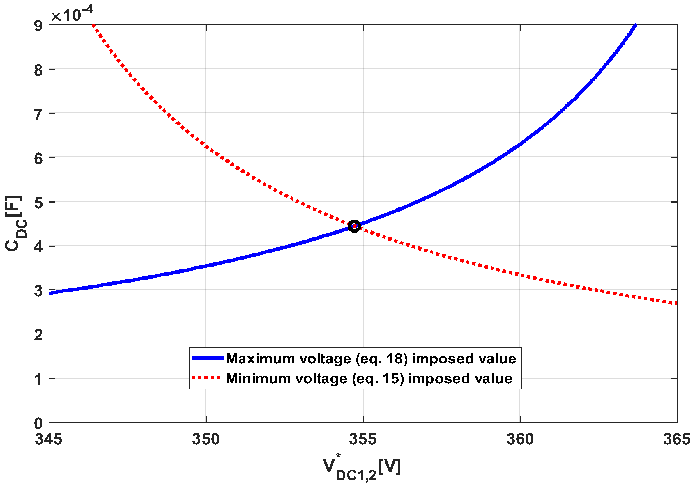
3. DC Link Capacitance Sizing
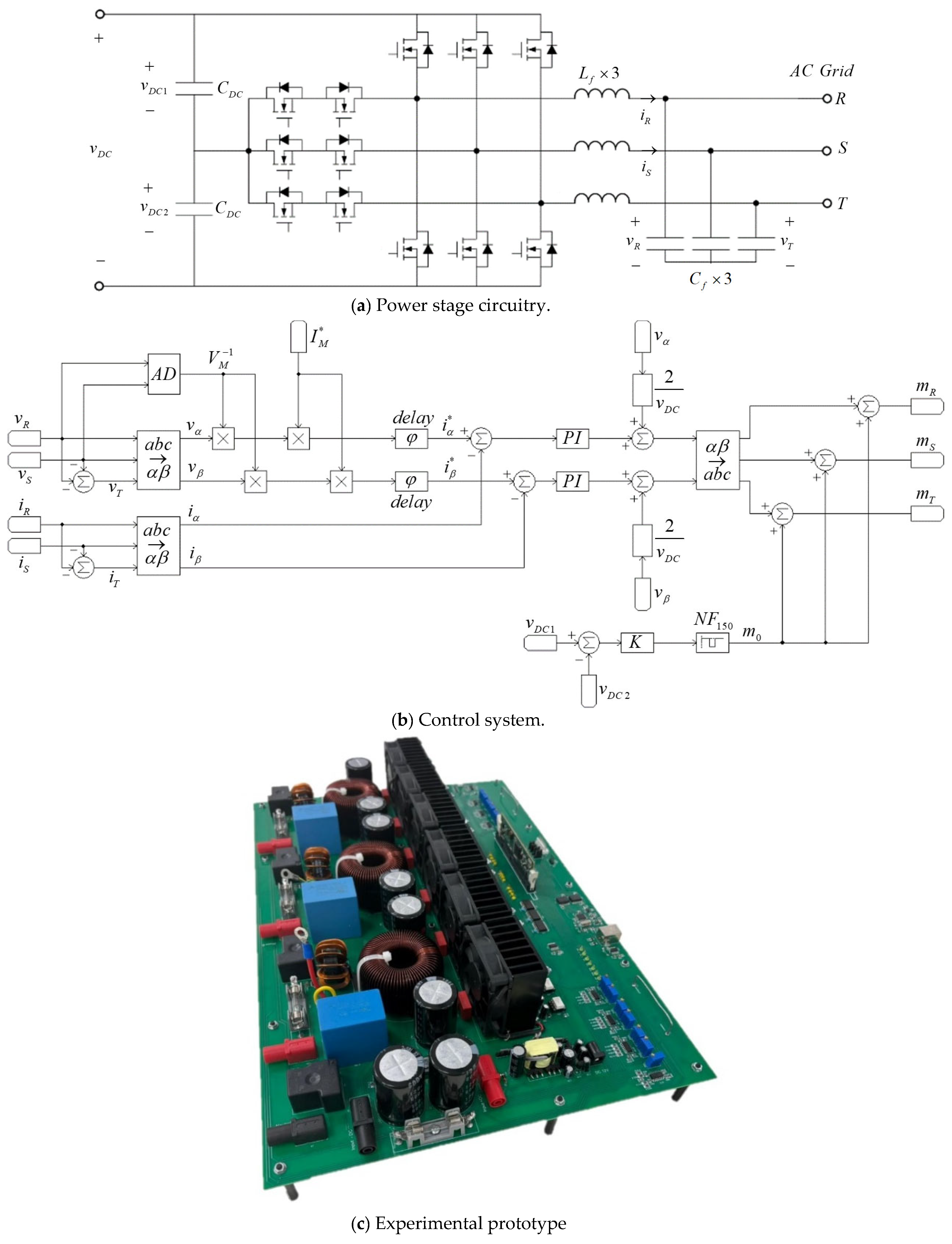
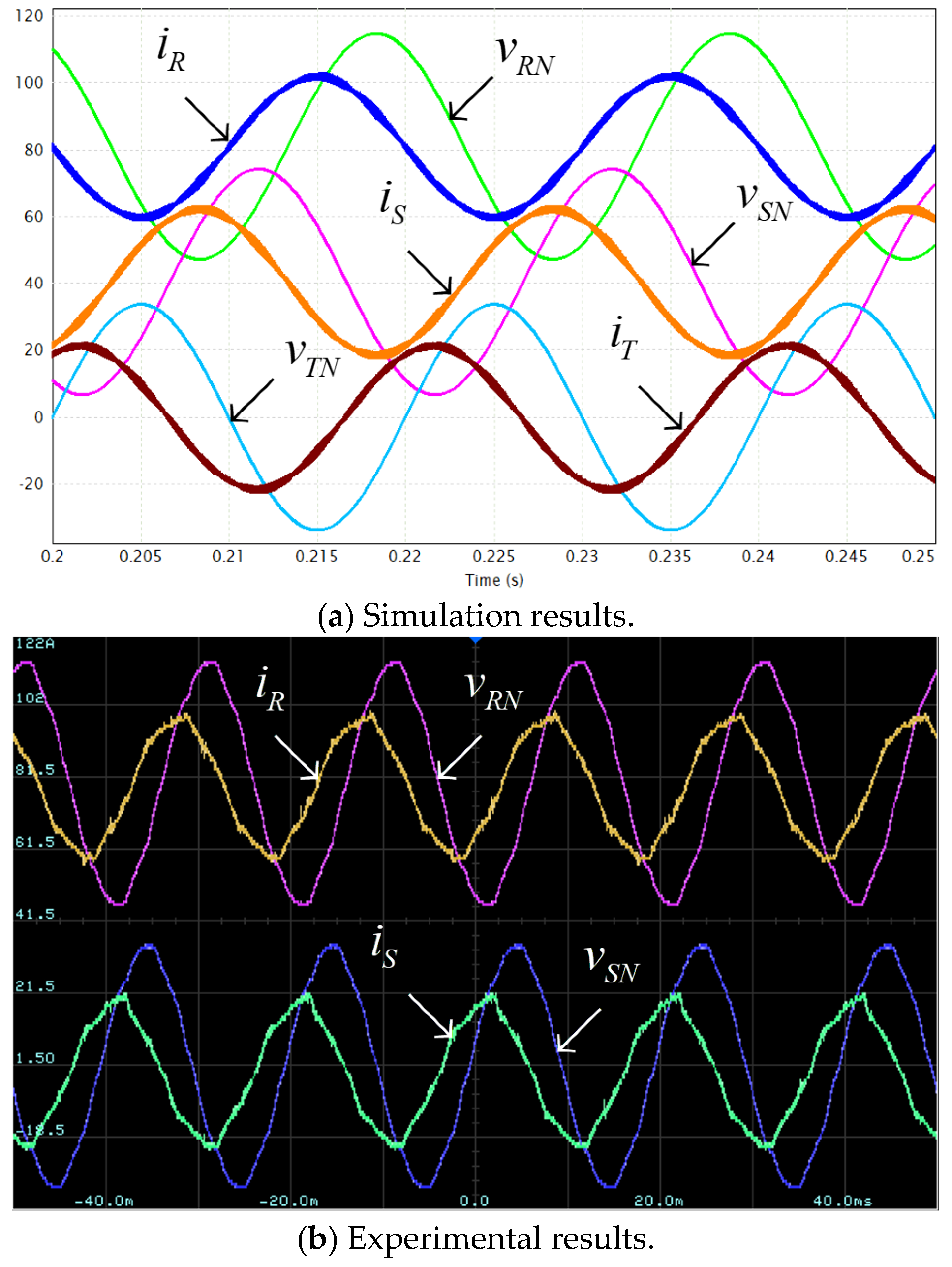
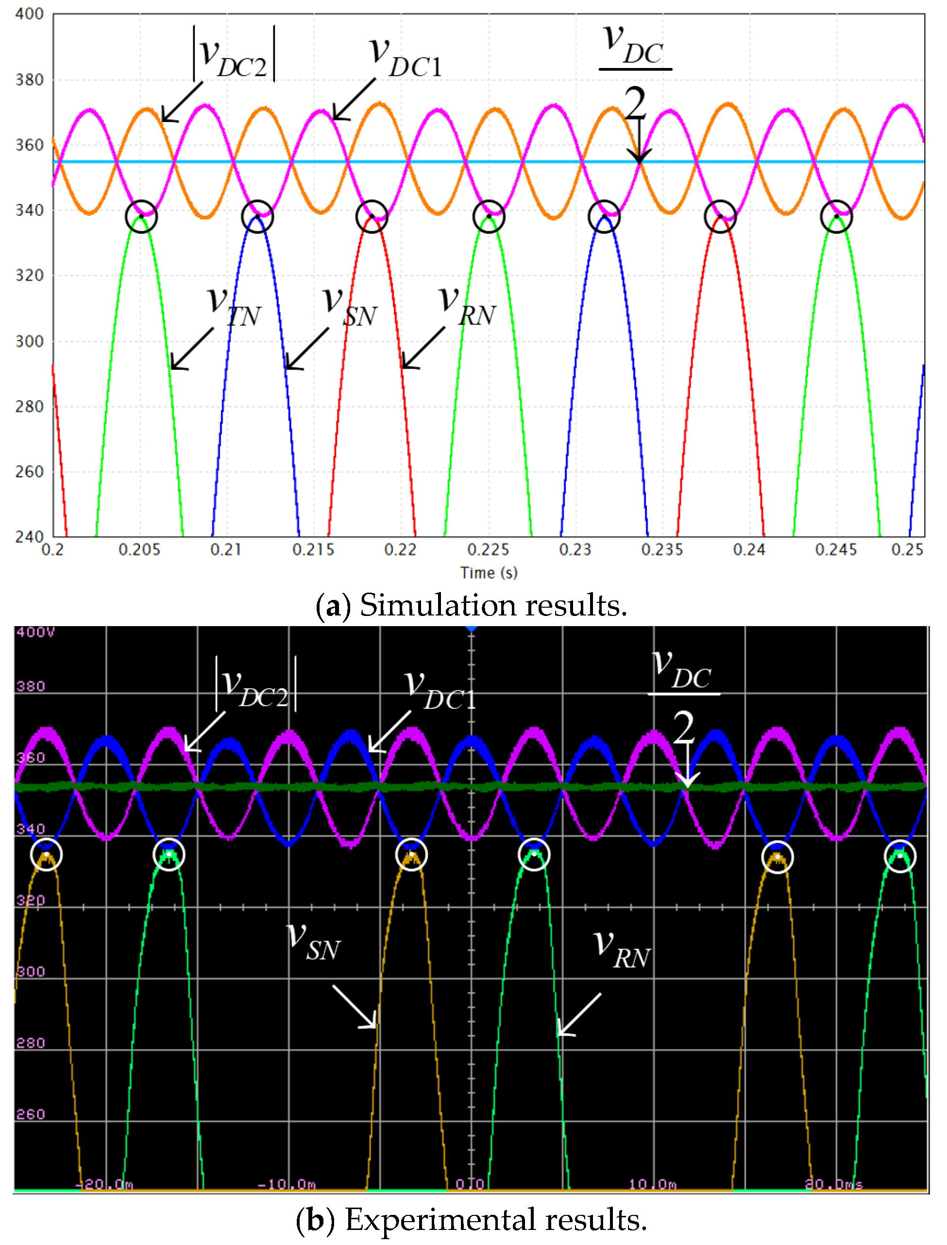
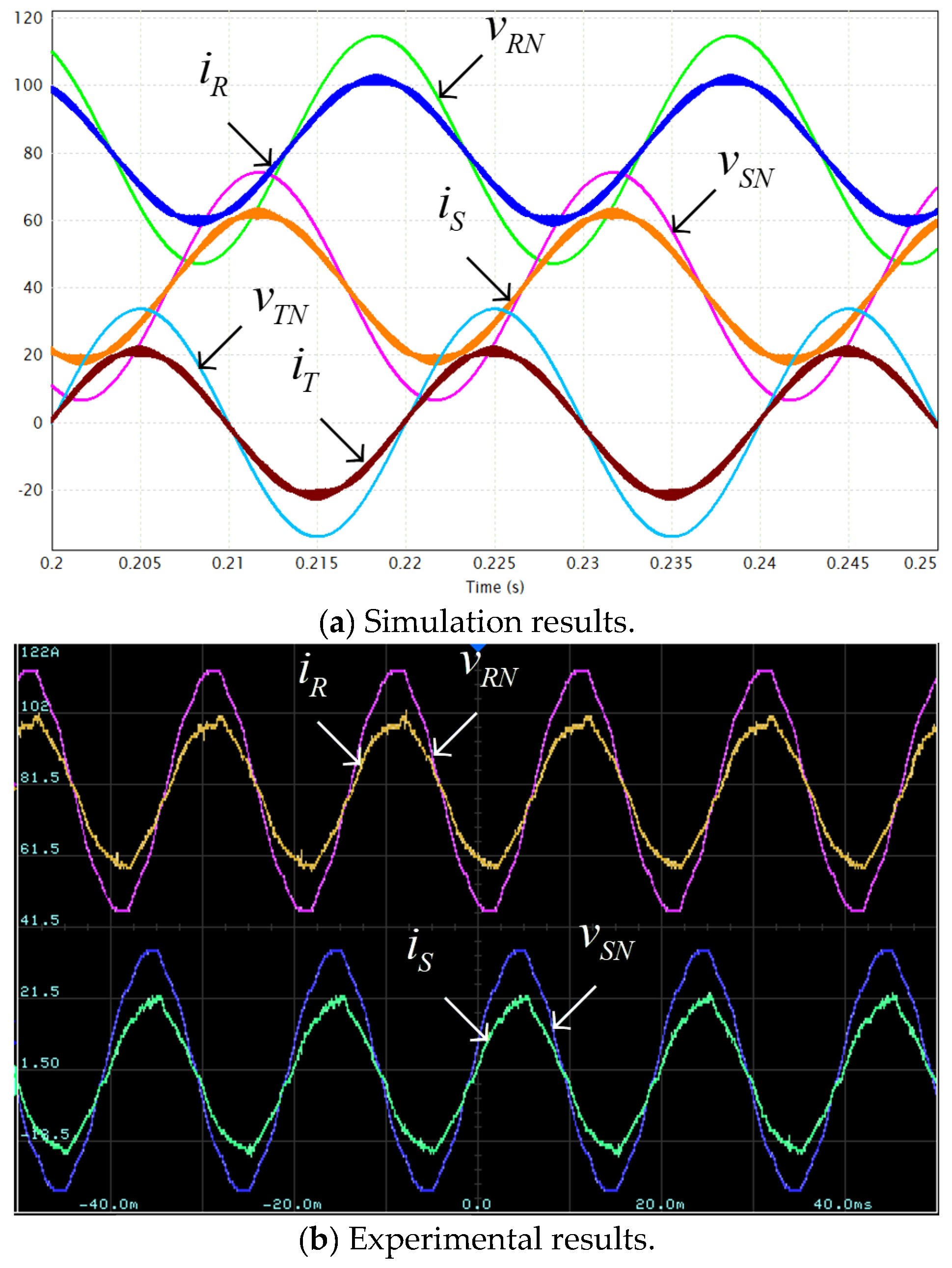
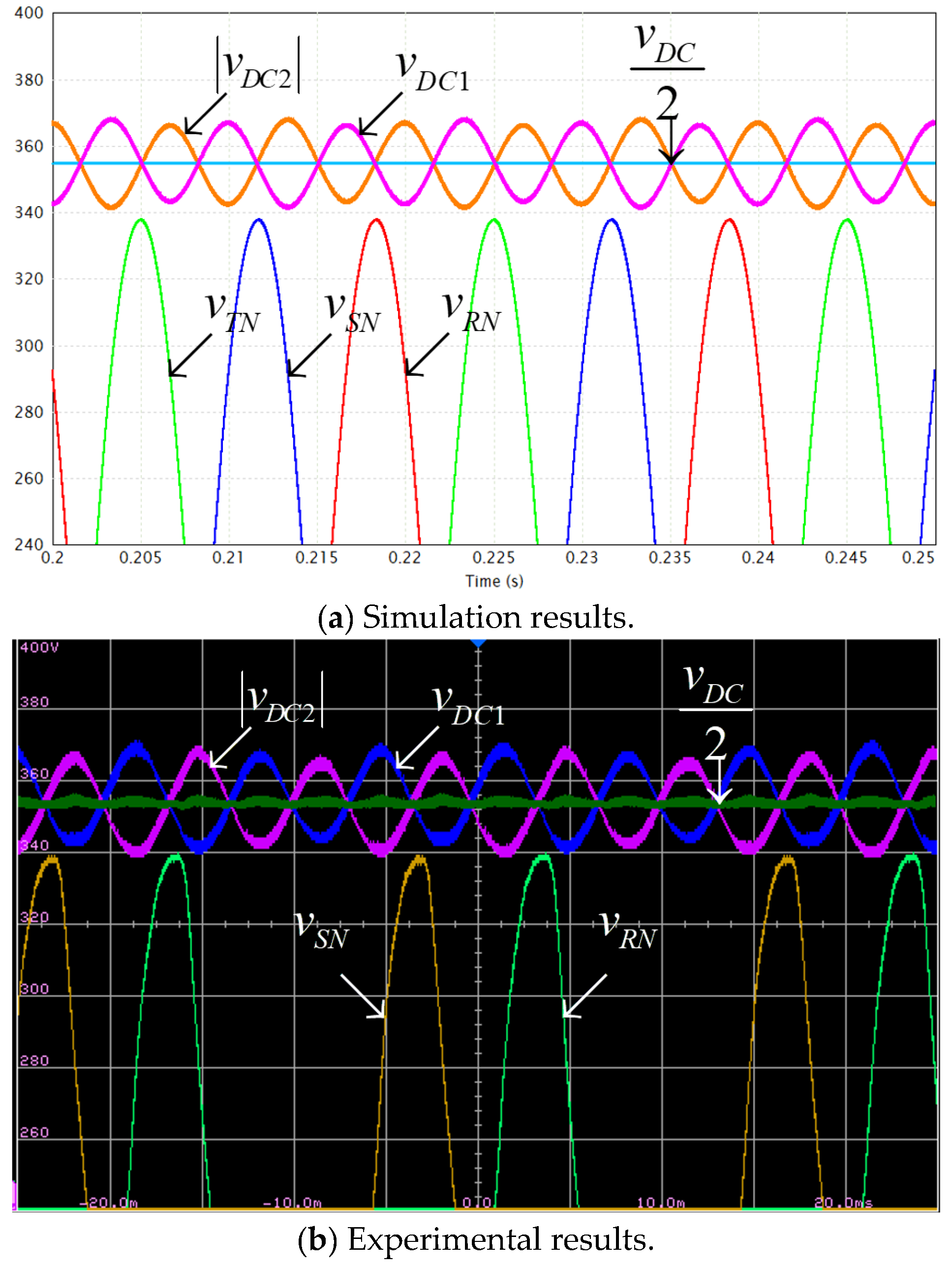
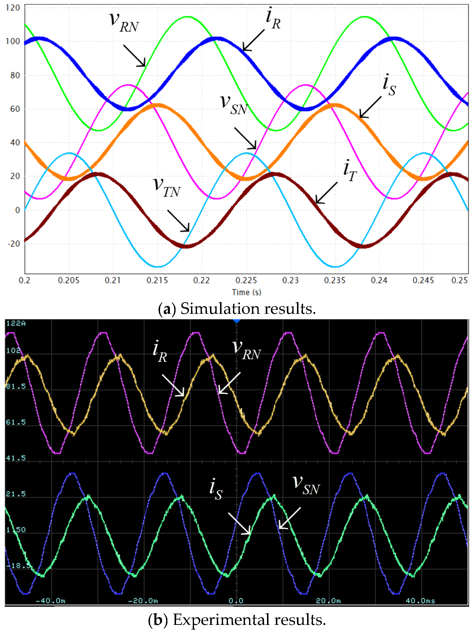
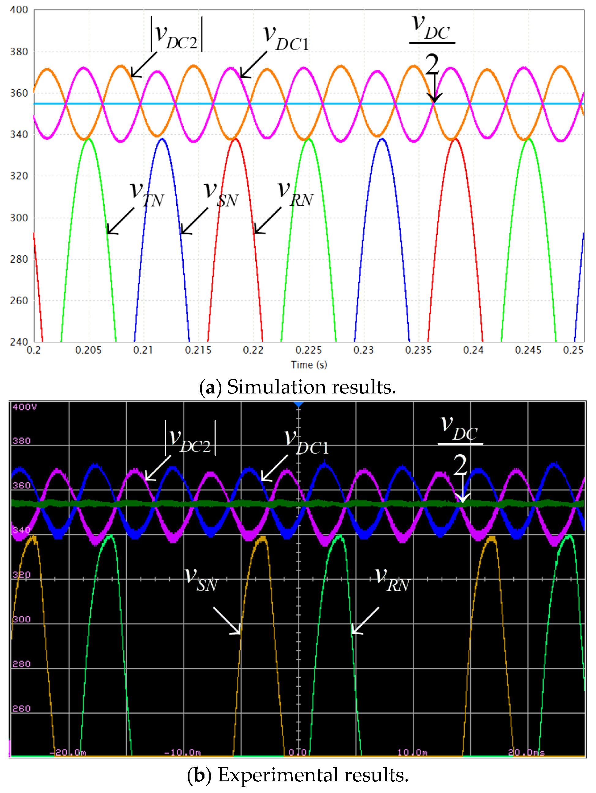
In order to assure correct functionality of the converter in Figure 2,
v R S T ( t ) v D C 1 , 2 ( t )
must hold instantaneously due to boost AC-to-DC (or buck DC-to-AC) topology of the latter. Combining the expressions of R-phase voltage (cf. (1)) and split DC-link voltage (cf. (7)), boundary condition satisfying (12) is given by
0.5 V D C * Δ V ( φ ) cos 3 ω t + α ( φ ) = V M sin ( ω t ) .
Equation (13) poses a challenge for obtaining an analytical solution in its original form yet may be solved numerically using any available computational software package. Nevertheless, it is possible to approximate the solution analytically by decomposing both sides of (13) into corresponding second-order Taylor series expansions, resulting in the following quadratic equation,
9 2 Δ V ( φ ) + V M 2 ( ω t ) 2 3 Δ V ( φ ) 2 π + α ( φ ) + π V M 2 ( ω t ) + + V D C * 2 + Δ V ( φ ) ( 2 π + α ( φ ) ) 2 2 1 V M 1 π 2 8 = 0 .
Figure 3 illustrates the accuracy of approximation (14). Since Taylor series expansions are carried out around corresponding peak points, the minimum error occurs when the power factor is zero and leading, while the maximum error arises when the power factor is zero and lagging. For a given range of expected power factors, the capacitance value of split DC link capacitors should be determined according to the lowest leading power factor (or the highest lagging power factor in case inductive-only operation is expected). Such a sizing approach guarantees correct performance within the whole operational power factor range while the proposed approximation provides a reliable method for calculating the minimum required capacitance value.
Boundary condition (13) is attained when the quadratic Equation (14) determinant equals zero, yielding a single solution (see [36] for additional details). Solving, minimum split DC link capacitance value is obtained as (cf. (9) and (10))
C D C = 288 S E A C p u V D C * 36 V D C * + V M ( 4 α 2 + 4 α π + π 2 80 ) + Δ
with given by
Δ = 1296 V D C * 2 + V D C * V M 288 α 2 + 288 α π + 72 π 2 4608 + + V M 2 16 α 4 + 32 α 3 π + 24 α 2 π 2 + 8 α π 3 + π 4 640 α 2 640 α π 160 π 2 + 4096 .
On the other hand, additional requirement should be established in practice in order to bound the maximum value of a split DC link capacitor voltage according to its voltage rating as follows. Denoting the voltage rating of a split DC link capacitor as VR, the maximum value of a split DC link capacitor voltage should be limited to kVR with k < 1 in order to provide a safety margin for prolonging the device lifetime. Consequently, the following equation is formed (cf. (8))
0.5 V D C * + Δ V ( φ ) = k V R ,
satisfied by a capacitor valued as (cf. (9))
C D C = S E A C p u ( φ ) 0.5 V D C * ( k V R 0.5 V D C * ) .
Combining (15) and (18) into
288 36 V D C * + V M ( 4 α 2 + 4 α π + π 2 80 ) + Δ = 2 k V R 0.5 V D C * .
and solving provides the required reference voltage value V D C * . Then, minimum split DC link capacitance value CDC may be obtained by substituting V D C * into (15) or (18).

4. Validation

In order to support the developed analytical split DC capacitor sizing framework experimentally, grid-connected LC-filter-based, three-phase three-level T-type AC-DC converter prototype depicted in Figure 4a was employed. Corresponding system parameters are summarized in Table 1. The converter was run at switching/sampling frequency of 50 kHz by means of the Texas Instruments control card based on the TMS320F28335 Digital Signal Processor. During the experimental framework, the T-type AC-DC converter was fed by a DC source (generating a constant-valued DC voltage vDC) while supplying a live three-phase AC grid with a set of balanced three-phase currents (cf. (1)) with controlled magnitudes and phase shifts.
The corresponding block diagram of the control system is shown in Figure 4b. In order to create in-phase unity-magnitude signal templates, grid voltages are sampled, Clarke-transformed into αβ domain and finally divided by grid voltage vector magnitude VM (obtained using amplitude detection block AD). The resulting unity-magnitude templates are multiplied by the desired grid current magnitude I M * and then delayed in order to impose the desired phase shift φ to create αβ domain current references i α * ,   i β * . On the other hand, grid currents were sampled, Clarke-transformed into αβ domain and subtracted from αβ domain current references i α * ,   i β * . Corresponding tracking errors were then processed by PI controllers. The outputs of αβ domain PI controllers were added to normalized αβ domain voltages (created by dividing αβ domain voltages vα, vβ by 0.5 vDC). The results were inverse-Clarke-transformed to create the first modulation signals term (at the right-hand side of (5)). Zero-sequence term m0 (i.e., the second term at the right-hand side of (5)) was generated by processing the difference between sampled split DC link voltages vDC1, vDC2 by a P + Notch controller employing a constant proportional gain K followed by a 150 Hz centered notch filter NF150 possessing unity DC gain aimed to suppress the triple-mains-frequency ripple (cf. (8)) in order to satisfy the DC-only zero sequence component constraint [35]. The experimental prototype is depicted in Figure 4c. Upon system start-up, the converter is synchronized with the AC grid and then grid-connected with zero-current reference. Then, the desired values of I M * and phase shift φ are imposed by the control system in order to bring the converter to the desired operating point. Measurements are performed when the system settles, and steady-state is attained.
Considering the range of power factors (both leading and lagging) given by
P F 0.5 ,
split DC link capacitances must be sized considering the lowest expected leading power factor (namely PF = −0.5 or φ = 60°, as discussed in the previous chapter and shown in Figure 3). Simultaneous solution of (15) and (18) with (9) and (10) (employing the values given in Table 1) yields the following values of split DC link voltage reference (19) and split capacitances, respectively. Corresponding graphical solution is depicted in Figure 5 for demonstration purposes. The ’minimum voltage-imposed value’ curve corresponds to Equation (15), while the ’maximum voltage-imposed value’ curve corresponds to (18). The values obtained in (20) are employed in both simulation and experimental frameworks as follows.
C D C 1 , 2 = 440   [ μ F ] ,     V D C 1 , 2 * = 355 [ V ]
Three simulations (PSIM 2025 software was used) and matching experiments were carried out under rated loading SR (cf. Table 1) under three following power factor values: PF = 0.5 (leading), PF = 1 (unity), PF = 0.5 (lagging) with the former representing the design point (cf. (21)). The results are depicted in Figure 6, Figure 7, Figure 8, Figure 9, Figure 10 and Figure 11. Experimental waveforms were acquired using a 4-channel oscilloscope, hence only two out of three AC-side quantities (i.e., two voltages and two currents) are shown simultaneously while all the three are given in corresponding simulation results. It should also be emphasized that due to the fact that the three-phase mains in the Applied Energy Laboratory (experimental site) is typically polluted with non-negligible harmonic content (well-evident in the experimental waveforms), the currents generated by the inverter also possess noticeable harmonic constituents due to simplified control system adopted (cf. Figure 4b) which does not consider harmonic elimination for brevity. Nevertheless, such characteristics do not affect the proposed methodology feasibility. It is well-evident that all simulation results accurately match their experimental counterparts even though the former consider purely sinusoidal AC-side voltage and currents.
Figure 6 and Figure 7 demonstrate operational waveforms of the system under rated loading with leading power factor of PF = 0.5 (i.e., AC-side currents lead corresponding AC-side voltages by 60°). It is well-evident that under these conditions, a single tangency point between positive part of grid voltages and positive split DC link voltage vDC1 exists, as indicated by black circles in Figure 7, as expected. On the other hand, split DC link voltages are kept below 376 V (=0.94∙400) at all time. Such a behavior accurately validates the design point (cf. (21)), simultaneously satisfying (15) and (18). Note that even though experimental waveforms of AC-side voltages are slightly distorted (due to harmonic content pollution), split DC link voltages are sinusoidal at triple-grid-frequency. This supports the above-made claim regarding negligible influence of AC-side current harmonic content on split DC-link voltages behavior particular and the proposed methodology feasibility in general. Similar conclusion may be drawn regarding operation under other power factor values as well. It is also evident that positive AC-side voltage peaks and valleys of split DC link voltage vDC1 are slightly shifted due to nonzero PF and are expected to approach each other in case the value of leading power factor is further decreased (cf. Figure 3). Figure 8 and Figure 9 demonstrate operational waveforms of the system under rated loading with unity power factor (here, AC-side currents are in-phase with corresponding AC-side voltages). It is well-evident that under these conditions no tangency point between positive grid voltage parts and the corresponding split DC link voltage vDC1 exists, as expected. On the other hand, split DC link voltages are kept below 376 V (=0.94∙400) at all times, as required. It is also evident that positive AC-side voltage peaks are synchronized with instances where vDC1 = −vDC2 = 0.5 vDC. Such a behavior is well in line with performance previously revealed by the Authors in [36]. Figure 10 and Figure 11 demonstrate operational waveforms of the system under rated loading with lagging power factor of PF = 0.5 (i.e., AC-side currents lag corresponding voltages by 60°). It is well-evident that under these conditions no tangency point between positive grid voltages parts and corresponding split DC link voltage vDC1 exists, as predicted. Split DC link voltages are kept below 376 V (=0.94∙400) at all times, as required. It is also evident that positive AC-side voltage peaks are nearly aligned with those of split DC link voltage vDC1 due to nonzero PF and are expected to approach each other in case the value of lagging power factor is further decreased (cf. Figure 3). Note that tangency between positive grid voltages and the absolute value of the split DC link voltage vDC2 is irrelevant. Consequently, operation under near-zero lagging power factor may be considered as “best case” while operation under near-zero leading power factor may be considered as “best case”.

5. Conclusions

A method for estimating the minimum split DC-link capacitance value required in a family of three-level, three-phase bidirectional AC-DC power converters operating with arbitrary power factor under constrained zero-sequence component was proposed and experimentally validated in the paper. The analysis is based on the previously revealed impact of arbitrary power factor operation on the behavior of split DC link voltages. A detailed examination of the distinction between operation with leading and lagging power factor and the corresponding influence on the capacitance sizing process was carried out. The proposed design approach was validated through closely matching simulations and experiments, confirming the accuracy of the developed analytical framework. Future work on the subject includes analysis of system operation under unbalanced AC-side voltages and/or nonlinear AC-side currents under both restricted and non-constrained zero-sequence injection.

Author Contributions

Conceptualization, A.K. and S.K.; methodology, Y.S., M.S., A.Y. and A.K.; software, Y.S. and V.Y.; validation, Y.S. and V.Y.; formal analysis, A.Y. and A.K.; investigation, Y.S. and M.S.; resources A.K.; data curation, Y.S. and V.Y.; writing—original draft preparation, Y.S.; writing—review and editing, A.Y. and A.K.; visualization, Y.S.; supervision, M.S., A.Y. and A.K.; project administration, S.K. and A.K.; funding acquisition, A.K. All authors have read and agreed to the published version of the manuscript.

Funding

This research was funded in part by the Israel Ministry of Energy.

Data Availability Statement

The original contributions presented in this study are included in the article. Further inquiries can be directed to the corresponding author.

Conflicts of Interest

The authors declare no conflicts of interest.

Nomenclature

v R S T ( t ) vector of grid voltages
V M grid voltages magnitude
φ currents vector angle With Respect To. voltages vector angle
i R S T ( t , φ ) vector of grid currents
I M grid currents magnitude
P F = cos φ power factor
S total apparent power
m R S T ( t ) vector of modulation indices
M ( t ) modulation indices magnitude
m 0 ( t ) zero-sequence modulation component
v D C ( t ) vector of partial DC link voltages
v D C 1 ( t ) , v D C 2 ( t ) individual partial DC link voltages
p R S T ( t , φ ) instantaneous AC-side phase power vector
p R S T ( t , φ ) total instantaneous AC-side power
v A B C ( t ) vector of converter imposed AC-side voltages
V D C * DC link voltage reference value
V D C 1 * , V D C 2 * split DC link set point voltages
C D C 1 , C D C 2 split DC link capacitances

References

  1. Bose, B.K. Multi-Level Converters. Electronics 2015, 4, 582–585. [Google Scholar] [CrossRef]
  2. Franquelo, L.G.; Leonand, J.; Rodriguez, J. The age of multilevel converters arrives. IEEE Ind. Electron. Mag. 2008, 2, 28–39. [Google Scholar] [CrossRef]
  3. Rodriguez, J.; Lai, J.-S.; Peng, F.Z. Multilevel inverters: A survey of topologies, controls, and applications. IEEE Trans. Ind. Electron. 2002, 49, 724–738. [Google Scholar] [CrossRef]
  4. Norões, M.; Jacobina, C.B.; Carlos, G.A. A new three-phase ac–dc–ac multilevel converter based on cascaded three-leg converters. IEEE Trans. Ind. Appl. 2017, 53, 2210–2221. [Google Scholar]
  5. Zhou, D.; Zhao, J.; Li, Y. Model-predictive control scheme of five-leg ac–dc–ac converter-fed induction motor drive. IEEE Trans. Ind. Electron. 2016, 63, 4517–4526. [Google Scholar] [CrossRef]
  6. Lima, M.; Cursino, B.J.; Rocha, N.; Santos, E.C. Ac–dc–ac three-phase converter based on three three-leg converters connected in series. IEEE Trans. Ind. Appl. 2016, 52, 3171–3181. [Google Scholar]
  7. Filho, S.; Cipriano, O.; de Almeida, B.R.; Souza, D.; Fernandes Neto, T.R. High-frequency isolated AC–DC–AC interleaved converter for power quality applications. IEEE Trans. Ind. Appl. 2018, 54, 4594–4602. [Google Scholar] [CrossRef]
  8. Norões, M.; Jacobina, C.B.; Freitas, N.B.; Queiroz, A.; Cabral Silva, E.R. Three-phase four-wire ac–dc–ac multilevel topologies obtained from an interconnection of three-leg converters. IEEE Trans. Ind. Appl. 2018, 54, 4728–4738. [Google Scholar]
  9. Norões, M.; Jacobina, C.B.; Freitas, N.B.; Alves Vitorino, M. Investigation of three-phase ac–dc–ac multilevel nine-leg converter. IEEE Trans. Ind. Appl. 2016, 52, 4156–4169. [Google Scholar]
  10. Kaufhold, E.; Meyer, J.; Schegner, P. Measurement-based identification of DC-link capacitance of single-phase power electronic devices for grey-box modelling. IEEE Trans. Power Electron. 2021, 37, 4544–4552. [Google Scholar]
  11. Khalil, A.; Ahmed, G.; Lee, D.C. DC-link capacitance estimation in AC-DC/AC PWM converters using voltage injection. IEEE Trans. Ind. Appl. 2008, 44, 1631–1637. [Google Scholar] [CrossRef]
  12. Divan, D.; Habetler, T.; Lipo, T. PWM techniques for voltage source inverters. In Proceedings of the IEEE PES Conference, Atlanta, GA, USA, 4–9 February 1990. [Google Scholar]
  13. Laszlo, H.; Kumar, M.; Jovanović, M.M. Performance comparison of three-step and six-step PWM in average-current-controlled three-phase six-switch boost PFC rectifier. IEEE Trans. Power Electron. 2016, 31, 7264–7272. [Google Scholar]
  14. Lu, Y.; Zhao, Z.; Lu, T.; Yang, S. An improved DC-link voltage fast control scheme for a PWM rectifier-inverter system. IEEE Trans. Ind. Appl. 2014, 50, 462–473. [Google Scholar]
  15. Xiong, X.; Zhang, Y.; Wang, J.; Du, H. An improved model predictive control scheme for the PWM rectifier-inverter system based on power-balancing mechanism. IEEE Trans. Ind. Electron. 2016, 63, 5197–5208. [Google Scholar]
  16. Sahraoui, K.; Gaoui, B. Reconfigurable control of PWM AC-DC-DC converter without redundancy leg supplying an ac motor drive. Period. Polytech. Electr. Eng. Comp. Sci. 2021, 65, 74–81. [Google Scholar] [CrossRef]
  17. Yanez-Campos, S.C.; Cerda-Villafana, G.; Lozano-Garcia, J.M. A two-grid interline dynamic voltage restorer based on two three-phase matrix converters. Appl. Sci. 2021, 11, 561. [Google Scholar] [CrossRef]
  18. Iqbal, A.; Lewicki, A.; Morawiec, M. Pulse-Width Modulation of Power Electronic DC–AC Converter. In High Performance Control of AC Drives with MATLAB®/Simulink, 2nd ed.; Wiley: Hoboken, NJ, USA, 2021. [Google Scholar]
  19. Stecca, M.; Soeiro, T.B.; Elizondo, L.R.; Bauer, P.; Palensky, P. Comparison of two and three-level DC-AC converters for a 100 kW battery energy storage system. In Proceedings of the ISIE Symposium, Delft, The Netherlands, 17–19 June 2020; pp. 677–682. [Google Scholar]
  20. Mellincovsky, M.; Yuhimenko, V.; Peretz, M.M.; Kuperman, A. Low-frequency DC-link ripple elimination in power converters with reduced capacitance by multiresonant direct voltage regulation. IEEE Trans. Ind. Electron. 2017, 64, 2015–2023. [Google Scholar] [CrossRef]
  21. Mutovkin, A.; Mellincovsky, M.; Yuhimenko, V.; Schacham, S.; Kuperman, A. Conditions for direct applicability of electronic capacitors to dual-stage grid-connected power conversion systems. IEEE J. Emerg. Sel. Top. Power Electron. 2019, 7, 1805–1814. [Google Scholar] [CrossRef]
  22. Baek, J.; Lee, J.-B.; Kim, J.-K. Effective hold-up time extension method using fan control in server power systems. IEEE Trans. Ind. Electron. 2020, 67, 5820–5824. [Google Scholar] [CrossRef]
  23. Huai, W.; Blaabjerg, F. Reliability of capacitors for DC-link applications in power electronic converters—An overview. IEEE Trans. Ind. Appl. 2014, 50, 3569–3578. [Google Scholar]
  24. Wang, H.; Wang, H.; Zhu, G.; Blaabjerg, F. An overview of capacitive DC links: Topology derivation and scalability analysis. IEEE Trans. Power Electron. 2019, 35, 1805–1829. [Google Scholar] [CrossRef]
  25. Wang, H.; Wang, H. Capacitive DC links in power electronic systems—Reliability and circuit design. Chin. J. Electr. Eng. 2018, 4, 29–36. [Google Scholar]
  26. Mutovkin, A.; Yuhimenko, V.; Schacham, S.E.; Kuperman, A. Simple and straightforward realization of an electronic capacitor. Electron. Lett. 2019, 55, 220–222. [Google Scholar] [CrossRef]
  27. Mutovkin, A.; Yuhimenko, V.; Mellincovsky, M.; Schacham, S.; Kuperman, A. Control of direct voltage regulated active DC-link capacitance reduction circuits to allow plug-and-play operation. IEEE Trans. Ind. Electron. 2019, 66, 6527–6537. [Google Scholar] [CrossRef]
  28. Mutovkin, A.; Yuhimenko, V.; Schacham, S.; Kuperman, A. Nonlinear control of electronic capacitor for enhanced stability and dynamic response. IEEE Trans. Ind. Electron. 2021, 68, 6881–6892. [Google Scholar] [CrossRef]
  29. Lamar, D.G.; Sebastian, J.; Arias, M.; Fernandez, A. On the limit of the output capacitor reduction in power factor correctors by distorting the line input current. IEEE Trans. Power Electron. 2012, 27, 1168–1176. [Google Scholar] [CrossRef]
  30. Hanson, A.J.; Martin, A.F.; Perreault, D.J. Energy and size reduction of grid-interfaced energy buffers through line waveform control. IEEE Trans. Power Electron. 2019, 34, 11442–11453. [Google Scholar] [CrossRef]
  31. Marcos-Pastor, A.; Vidal-Idiarte, E.; Cid-Pastor, A.; Martinez-Salamero, L. Minimum DC-link capacitance for single-phase applications with power factor correction. IEEE Trans. Ind. Electron. 2020, 67, 5204–5208. [Google Scholar] [CrossRef]
  32. Strajnikov, P.; Kuperman, A. On the minimum DC link capacitance in practical PFC rectifiers considering THD requirements and load transients. IEEE Trans. Ind. Electron. 2022, 69, 11067–11075. [Google Scholar] [CrossRef]
  33. Krein, P.T.; Balog, R.S.; Mirjafari, M. Minimum energy and capacitance requirements for single-phase inverters and rectifiers using a ripple port. IEEE Trans. Power Electron. 2012, 27, 4690–4698. [Google Scholar] [CrossRef]
  34. Strajnikov, P.; Kuperman, A. DC link capacitance reduction in PFC rectifiers employing PI+Notch voltage controllers. IEEE Trans. Power Electron. 2023, 38, 977–986. [Google Scholar] [CrossRef]
  35. Siton, Y.; Yuhimenko, V.; Baimel, D.; Kuperman, A. Baseline for split DC-link design in three-phase three-level converters operating with unity power factor based on low-frequency partial voltage oscillations. Machines 2022, 10, 722. [Google Scholar] [CrossRef]
  36. Siton, Y.; Sitbon, M.; Aharon, I.; Lineykin, S.; Baimel, D.; Kuperman, A. On the minimum value of split DC link capacitances in three-phase three-level grid-connected converters operating with unity power factor with limited zero-sequence Injection. Electronics 2023, 12, 1994. [Google Scholar] [CrossRef]
  37. Siton, Y.; Kuperman, A. Generalization of split DC link voltages behavior in three-phase-level converters operating with arbitrary power factor with restricted zero-sequence component. Electronics 2023, 12, 4063. [Google Scholar] [CrossRef]
Figure 1. Dual stage power conversion system under consideration.
Applsci 15 03159 g001
Figure 2. Generalized topology of a three-level three-phase AC-DC power converter.
Applsci 15 03159 g002
Figure 3. Positive split DC link capacitance voltage and AC-side phase voltage for three values of cos φ employing corresponding minimum values of split DC link capacitances.
Applsci 15 03159 g003
Figure 4. System used for methodology verification.
Applsci 15 03159 g004
Figure 5. Graphical solution of (15) and (18) to obtain (20).
Applsci 15 03159 g005
Figure 6. AC-side currents and voltages. Rated load, cos φ = 0.5 (leading). Voltage scale: 200 V/div; Current scale: 20 A/div; Time scale: 5 ms/div.
Applsci 15 03159 g006
Figure 7. AC-side and DC-side voltages. Rated load, cos φ = 0.5 (leading). Voltage scale: 20 V/div; Time scale: 5 ms/div.
Applsci 15 03159 g007
Figure 8. AC-side currents and voltages. Rated load, cos φ = 1 . Voltage scale: 200 V/div; Current scale: 20 A/div; Time scale: 5 ms/div.
Applsci 15 03159 g008
Figure 9. AC-side and DC-side voltages. Rated load, cos φ = 1 . Voltage scale: 20 V/div; Time scale: 5 ms/div.
Applsci 15 03159 g009
Figure 10. AC-side currents and voltages. Rated load, cos φ = 0.5 (lagging). Voltage scale: 200 V/div; Current scale: 20 A/div; Time scale: 5 ms/div.
Applsci 15 03159 g010
Figure 11. AC-side and DC-side voltages. Rated load, cos φ = 0.5 (lagging). Voltage scale: 20 V/div; Time scale: 5 ms/div.
Applsci 15 03159 g011
Table 1. System parameter values.
ParameterValueUnits
V M 240 2 V
ω 2 π · 50 r a d / s
L f 350 μ H
C f 10 μ F
ESR( L f 1 )50 m Ω
ESR( C f )316 m Ω
SR11kVA
V R 400V
k0.94-
min(PF)0.5 Leading/Lagging-
Disclaimer/Publisher’s Note: The statements, opinions and data contained in all publications are solely those of the individual author(s) and contributor(s) and not of MDPI and/or the editor(s). MDPI and/or the editor(s) disclaim responsibility for any injury to people or property resulting from any ideas, methods, instructions or products referred to in the content.

