Article

RHLP-18T: A Radiation-Hardened 18T SRAM with Enhanced Read Stability and Low Power Consumption

Department of Semiconductor Engineering, Tech University of Korea, Siheung 15073, Republic of Korea
*
Author to whom correspondence should be addressed.
Appl. Sci. 2025, 15(10), 5712; https://doi.org/10.3390/app15105712
Submission received: 20 April 2025 / Revised: 13 May 2025 / Accepted: 18 May 2025 / Published: 20 May 2025

Abstract

:
Electronic equipment in space is constantly exposed to high-energy particles, which can induce Single Event Upsets (SEUs) in memory components, threatening system reliability. To address this critical challenge, we propose RHLP-18T, a radiation-hardened 18-transistor (18T) Static Random-Access Memory (SRAM) cell designed to enhance robustness against radiation-induced faults. The proposed cell integrates circuit-level Radiation-Hardened-by-Design (RHBD) techniques to mitigate both SEUs and multi-node upsets. Comprehensive simulations were conducted using 90 nm CMOS technology, benchmarking RHLP-18T against nine existing RHBD cells (RHBD14T, HPHS12T, NRHC14T, QCCS12T, RHMC12T, RHWC12T, SEA14T, SIMR-18T, and SERSC16T). Simulation results demonstrate that the proposed RHLP-18T cell exhibits superior SEU tolerance, achieving a Read Static Noise Margin (RSNM) over three times higher than the next best design. Moreover, the proposed cell achieves the lowest hold power consumption among all evaluated cells. These improvements result in the highest Figure of Merit (FOM), indicating that RHLP-18T provides an optimal trade-off between robustness and overall performance for operation in radiation-exposed environments.

1. Introduction

Aerospace systems and terrestrial applications operating at high altitudes face harsh environments, where high-energy particle interactions significantly threaten electronic component reliability. Sources like Galactic Cosmic Rays (GCR), solar particle events, and trapped radiation belts expose circuits to a flux of heavy ions, protons, and other energetic particles [1]. When such a particle passes through a Metal–Oxide–Semiconductor (MOS) transistor within a Static Random-Access Memory (SRAM) cell, it deposits energy along its path. This instantly generates a dense track of electron–hole pairs. The deposited charge can then be collected by sensitive nodes within the cell through mechanisms like drift and diffusion or the parasitic bipolar amplification effect [2]. If this collected charge exceeds a critical threshold, it can induce a transient pulse or cause a persistent state flip—a Single Event Upset (SEU)—altering the stored logic state (e.g., ‘0’ flipping to ‘1’) [3]. The charge collection dynamics induced by high-energy particles are critically dependent on the Linear Energy Transfer (LET)—a measure of energy deposition per unit path length by ionizing radiation—and device architecture. In advanced nanometer-scale FinFET (Field Effect Transistor) technologies, the three-dimensional gate structure enhances charge collection efficiency through pronounced funneling effects, consequently increasing SEU susceptibility compared to planar transistor architectures. These radiation-induced mechanisms must be rigorously addressed in radiation-hardened circuit design to ensure reliable operation in harsh environments [4]. Depending on the system’s criticality, such SEUs in memory can lead to data corruption, erroneous computations, loss of control, and potentially mission failure. Therefore, SRAM cells used in these demanding applications must employ specialized Radiation-Hardened-by-Design (RHBD) approaches to ensure data integrity and system survivability [5].
RHBD technology is important not only for aerospace applications but also for nuclear power systems. Robots and control systems deployed inside nuclear power plants or at nuclear accident sites are continuously exposed to intense radiation, making them susceptible to radiation-induced errors such as SEUs, like in space environments. To mitigate these risks, RHBD techniques with robustness equivalent to those used in aerospace systems are indispensable [6].
To counter the harmful effects of radiation, the research community has spent decades developing a wide range of RHBD strategies [7,8]. These strategies fall into several broad categories. Process-level hardening involves modifying the semiconductor manufacturing process itself, for instance, using Silicon-On-Insulator (SOI) substrates to reduce sensitive charge collection volume or employing specific doping profiles [9]. Layout-level techniques focus on the physical arrangement of transistors and interconnects; examples include implementing guard rings to suppress a Single Event Latch-up (SEL), increasing spacing between sensitive nodes to reduce charge sharing, and using redundant contacts. Complementary to these are circuit-level RHBD techniques, which modify the cell’s electrical design to inherently tolerate or correct for SEUs [10]. These often involve adding transistors to create redundancy, implement error detection/correction, or enhance storage node stability. This work falls into the latter category, presenting a newly developed SRAM bit-cell architecture, which is designated as RHLP (Radiation-Hardened Low-Power)-18T in this paper.
The RHLP-18T cell architecture presented in this paper is designed primarily for high SEU robustness, excellent read stability, and low static (hold) power consumption. While many established RHBD SRAM cells prioritize minimizing transistor count for area efficiency (e.g., various 12T or 14T designs), these approaches can involve compromises in noise margins or exhibit vulnerabilities to specific SEU scenarios or multiple-node charge collection events. In contrast, proposed RHLP-18T structure uses its increased circuit complexity (18 transistors) to significantly enhance both data stability and SEU tolerance beyond what is typically achievable with lower-transistor-count designs. We strategically incorporated additional transistors not just for passive redundancy but also to actively strengthen feedback loops and effectively isolate sensitive internal nodes during upsets. By prioritizing major improvements in read stability and hold power—often critical metrics for overall system performance and energy budget—proposed design acknowledges and balances the inherent trade-offs between speed, power, noise margin, and radiation hardness in the SRAM design. This paper details the RHLP-18T architecture, analyzes its operational principles, presents simulation results demonstrating its performance and SEU robustness, and provides a comparative evaluation against relevant existing RHBD cell designs.
The proposed integrated circuit was implemented using a 90 nm CMOS process, operating at a supply voltage of 1 V. A comparative evaluation was performed against existing RHBD SRAM cells under identical simulation settings: RHBD14T [11], HPHS12T [12], NRHC14T [13], QCCS12T [14], RHMC12T [15], RHWC12T [16], SEA14T [17], SIMR18T [18], and SERSC16T [19].

2. Proposed RHLP-18T Cell and Its Operations

This section describes the structure and operating principles of the proposed RHLP-18T cell. The schematic and layout of proposed RHLP-18T cell are shown at Figure 1 and Figure 2. The operating principle of the circuit in Figure 1 is explained in Section 2.1. The cell consists of 12 PMOS and 6 NMOS transistors, totaling 18 transistors. Regarding key transistor sizing, the width of the primary pull-down NMOS transistors (N1, N2, N3, N4) connected to the storage nodes (Q, QB) was set to twice the minimum design rule size (2 × Wmin), specifically to enhance the Read Static Noise Margin (RSNM). The width of core PMOS transistors P3 and P4 was set to three times the minimum size (3 × Wmin) to strengthen the SEU recovery mechanism. These values were obtained through simulations to enhance RSNM and the SEU recovery mechanism. All other transistors within the cell utilize the minimum feature size (Wmin) allowed by the 90 nm CMOS process technology.

2.1. Memory Operation of the Proposed RHLP-18T Cell

2.1.1. Hold Mode

During the hold mode, the memory cell maintains its stored data without external access by deactivating access transistors (N5, N6, P11, P12). This is achieved by setting the word line (WL) to ground (GND) and the write word line (WWL) to the supply voltage (VDD). Consider the case where the cell stores a logic ‘1’ (internal node Q = 1 and QB = 0). In this state, P4, P5, P6, P8, P9, N1, and N3 are on, while P1, P2, P3, P7, P10, N2, and N4 are off. This transistor configuration ensures the internal storage nodes (Q and QB) maintain their states.

2.1.2. Read Mode

For a read operation, both bit lines (BL and BLB) are typically precharged to VDD. Subsequently, both WL and WWL are driven to VDD, which activates the NMOS access transistors N5 and N6 but keeps the PMOS write-assist transistors P11 and P12 deactivated. When the cell stores a logic ‘1’ (Q = 1, QB = 0), bit line BL, connected to node Q via N6, remains high. This state is primarily maintained by the active pull-up transistor P4 (see Figure 1). Simultaneously, bit line BLB, connected to node QB via N5, begins to discharge toward ground. This discharge occurs through the conductive path formed by transistors N5, N1, and N3, which are active when Q = 1. The resulting voltage difference between BL and BLB is detected by a connected sense amplifier to read the stored data.

2.1.3. Write Mode

The write operation is initiated by driving WL to VDD and WWL to GND, activating all access transistors (N5, N6, P11, P12). Consider writing a ‘0’ into a cell currently storing ‘1’ (Q = 1, QB = 0), for which BL is driven to GND and BLB to VDD. Node Q is pulled down towards ‘0’ as the active access transistor N6 provides a path to BL (GND). Simultaneously, node QB is pulled up toward ‘1’ as the active write-assist transistor P11 provides a strong path to BLB (VDD). These driving actions through the activated transistors directly force the storage nodes Q and QB to flip their states, thereby completing the write ‘0’ operation. The three operating states—hold, read, and write—are illustrated in the memory operation waveforms shown in Figure 3.

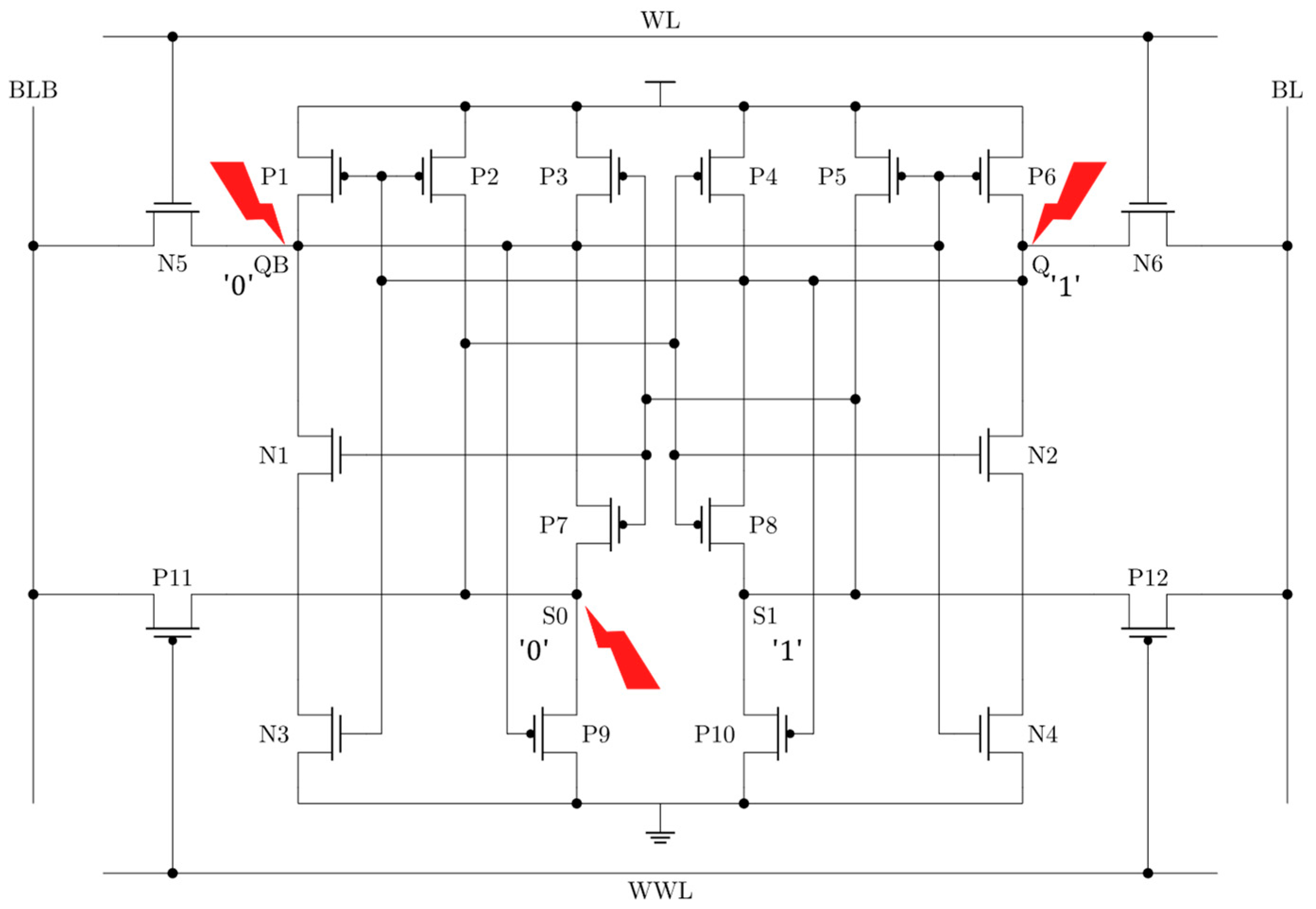
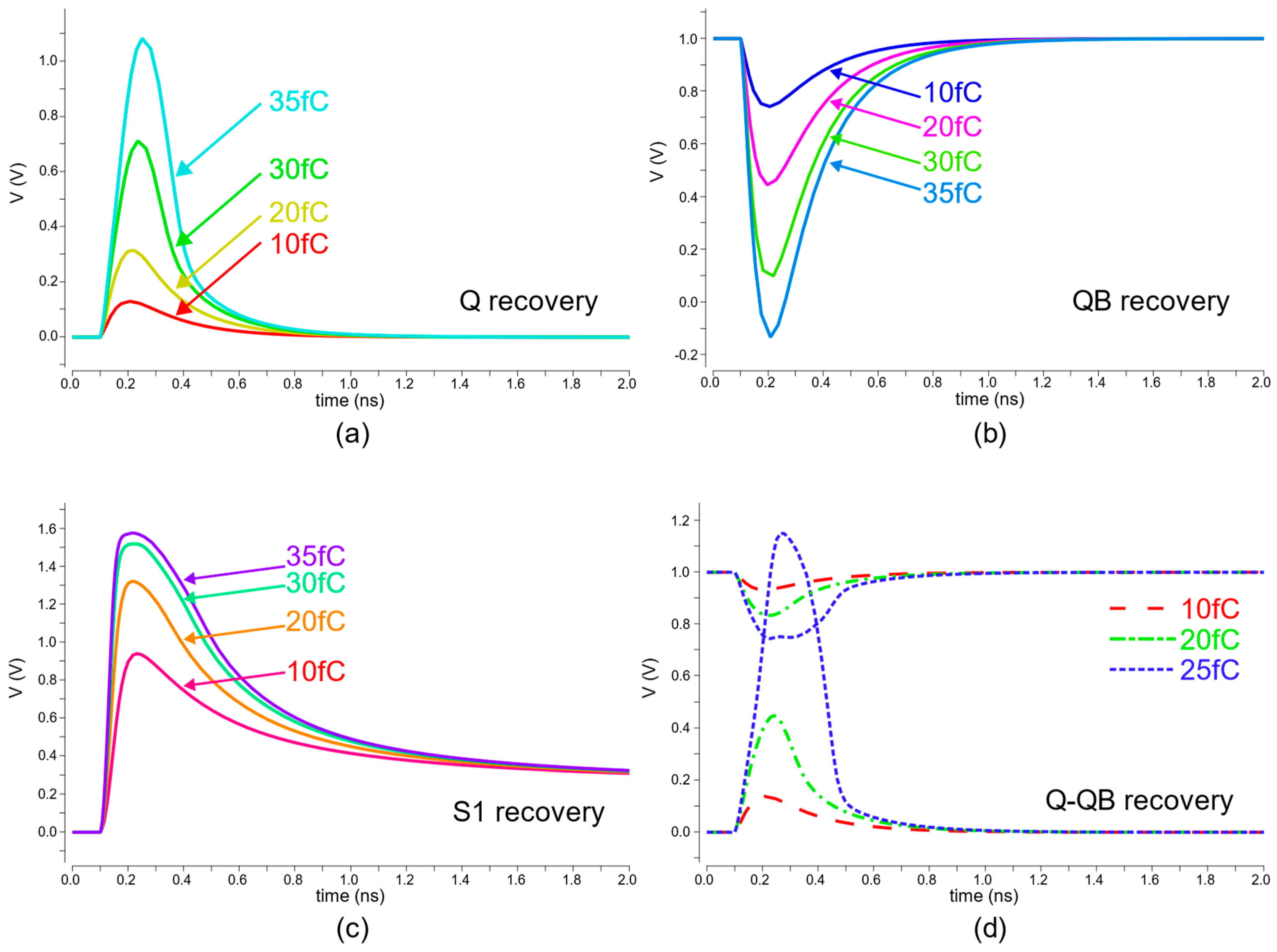
2.2. Radiation-Hardened SEU Recovery Analysis

When a high-energy particle strikes an NMOS, a negative current is generated. This can induce a 0-to-0 or 1-to-0 upset. In the case of a PMOS, a positive current is generated, which can induce a 1-to-1 or 0-to-1 upset. When the RHLP-18T cell stored at logic 1, nodes Q, QB, and S0 are considered sensitive nodes because a 1-to-0 upset or 0-to-1 upset can occur as shown in Figure 1. The RHLP-18T cell includes mechanisms to recover from single-node upsets caused by particle strikes hitting sensitive nodes.
(1)
When a high-energy particle strike momentarily flips node Q from ‘1’ down to ‘0’, this turns on transistors P1 and P2, and it turns off N3, causing node QB’s voltage to rise. Crucially, transistor P3 is designed with significantly more pull-up strength than P1 (approximately three times greater). This difference ensures that node Q is quickly pulled back up to logic ‘1’ before the related nodes (S0 and S1) can fully change state. This rapid restoration prevents the upset from corrupting stored data.
(2)
When a high-energy particle strike flips node QB from ‘0’ up to ‘1’, this turns off P5, P6, and P9, and turns on N4. Node S0 briefly enters a high-impedance state but effectively stays at logic ‘0’. As a result, N2 remains off, shielding primary storage node Q from the disturbance. The transient upset at QB does not manage to flip Q. Afterward, QB is pulled back down to logic ‘0’ through the path provided by N1 and N3 (which are on because Q = 1).
(3)
When a high-energy particle strike flips node S0 from ‘0’ to ‘1’, transistors P4 and P8 turn off, while N2 turns on. As a result, node S1 floats, and node Q also temporarily floats because N4 is off. Despite these transient disruptions, the main latch (Q/QB) does not flip its state. Node S0 is then pulled back to logic ‘0’ by transistor P9, which connects it to QB (normally at logic ‘0’).
(4)
When a single event strike simultaneously flips node Q from ‘1’ to ‘0’ and node QB from ‘0’ to ‘1’, the design ensures that the restoring pull-up strength of P3 (driving Q high) overcomes the combined pull-down strength attempting to keep Q low. This pull-down involves N2 and N4, depending on the transient states of S0 and S1. Because the pull-up is stronger, node Q recovers to logic ‘1’ before the secondary nodes S0 and S1 fully invert, successfully restoring the original state.
(5)
When a high-energy particle simultaneously strikes the sensitive nodes Q-S0 or QB-S0, an upset occurs from 1–0 to 0–1 in Q-S0, and from 0–0 to 1–1 in QB-S0. This turns on P1, P2, P4, P8, N4 and turns off P3, P7, P5, P6, N3. In this case, all storage nodes change and are unrecoverable. According to [7], to prevent the charge-sharing effect, the distance between transistors (PMOS to PMOS and PMOS to NMOS) connected to the sensitive nodes must be at least 0.6 um. Accordingly, the layout was designed with a distance of 0.85 um between P1 and P2, and a distance of 3.71 um between P7 and N2, as shown in Figure 2.
In summary, the RHLP-18T cell has three main sensitive nodes (Q, QB, S0). The design inherently recovers from SEUs at all these nodes and Single Event Double Node Upset (SEDNU) at Q-QB nodes, as shown in Figure 4. The layout design prevents SEDNU at Q-S0 and QB-S0 nodes.

3. Simulation Results and Analysis

This section presents the simulation setup and compares the performance of the proposed RHLP-18T cell with that of reference designs, with an emphasis on key SRAM metrics. All simulations were conducted using a standard 90 nm CMOS process technology with a supply voltage (VDD) of 1 V and an operating temperature set to 27 °C. To ensure a fair comparison, the reference RHBD cells [7,8,9,10,11,12,13,14,15] were reconstructed based on the schematics and transistor dimensions described in their respective publications. Any dimensions not specified in the original papers were set to the minimum feature size allowed by the 90 nm process. The proposed RHLP-18T cell was implemented according to the design details presented in Section 2.

3.1. Stability Comparison

The Static Noise Margin (SNM) is a key measure of how stable a memory cell is against DC noise. It tells us the minimum DC noise voltage needed to flip the cell’s stored state. The Static Noise Margin (SNM) is evaluated in three operating modes: hold (HSNM), read (RSNM), and write (WSNM).

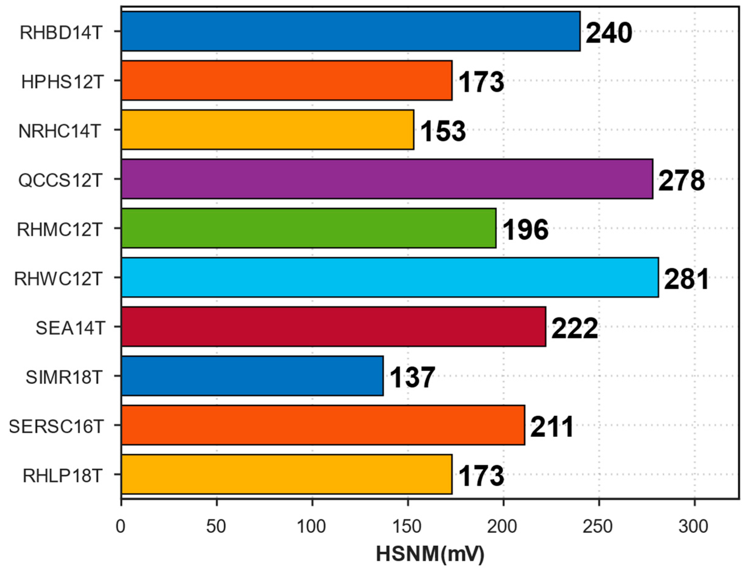
3.1.1. HSNM Comparison

The Hold Static Noise Margin (HSNM) is obtained by plotting the Voltage Transfer Characteristics (VTCs) of the cross-coupled inverters while the cell is in the hold state. This creates a “butterfly curve”, and the HSNM is the side length of the largest square that fits inside the curve’s two lobes. As Figure 5 shows, the RHLP-18T has an HSNM of 173 mV. This is somewhat lower than cells like QCCS12T (278 mV) and RHWC12T (281 mV), though better than SIMR18T (137 mV). This moderate HSNM might be due to the cell’s longer internal feedback paths and the weaker nodes created by transistors P9 and P10 compared to a standard 6T cell—representing a likely trade-off to improve other characteristics.

3.1.2. RSNM Comparison

The RSNM is obtained by generating the butterfly curve under read operation conditions (WL = VDD, WWL = VDD, BL/BLB precharged). In the same way as HSNM, RSNM is defined as the side length of the largest square that fits between the curves. Here, the proposed RHLP-18T exhibits an RSNM of 150 mV. This value is significantly higher than those of the compared cells (Figure 6), where the next highest RSNM observed was 49 mV (RHBD14T). This notable improvement in read stability—although potentially contributing to the slower Read Access Time (RAT), discussed in Section 3.2—is a significant advantage for noise-prone environments. The high RSNM appears to result from a combination of factors inherent in the RHLP-18T design:
(1)
Write Path Decoupling via WWL: The use of the separate Write Word Line (WWL) helps maintain stability during reads. By setting WWL to VDD, the PMOS write access transistors (P11, P12) are turned off. This effectively decouples the write circuitry from the storage nodes and bit lines during the read operation, preventing potential interference or loading effects from the write transistors.
(2)
Robust Core Latch and Cell Ratio: The core latch structure’s robustness is enhanced by its design, including the relative sizing of driver and access transistors, often characterized by the Cell Ratio (CR). In this design, the primary pull-down NMOS transistors (N1, N2, N3, N4) have a width twice the minimum size. Assuming the read access transistors (N5, N6) are minimum size, this results in an effective Cell Ratio (CR) of approximately 2. This relatively high CR enhances the latch’s ability to hold its state during a read operation, contributing significantly to the high RSNM.
(3)
Cell Characteristics: A large internal voltage swing during operation likely also contributes to the enhanced read stability margin.

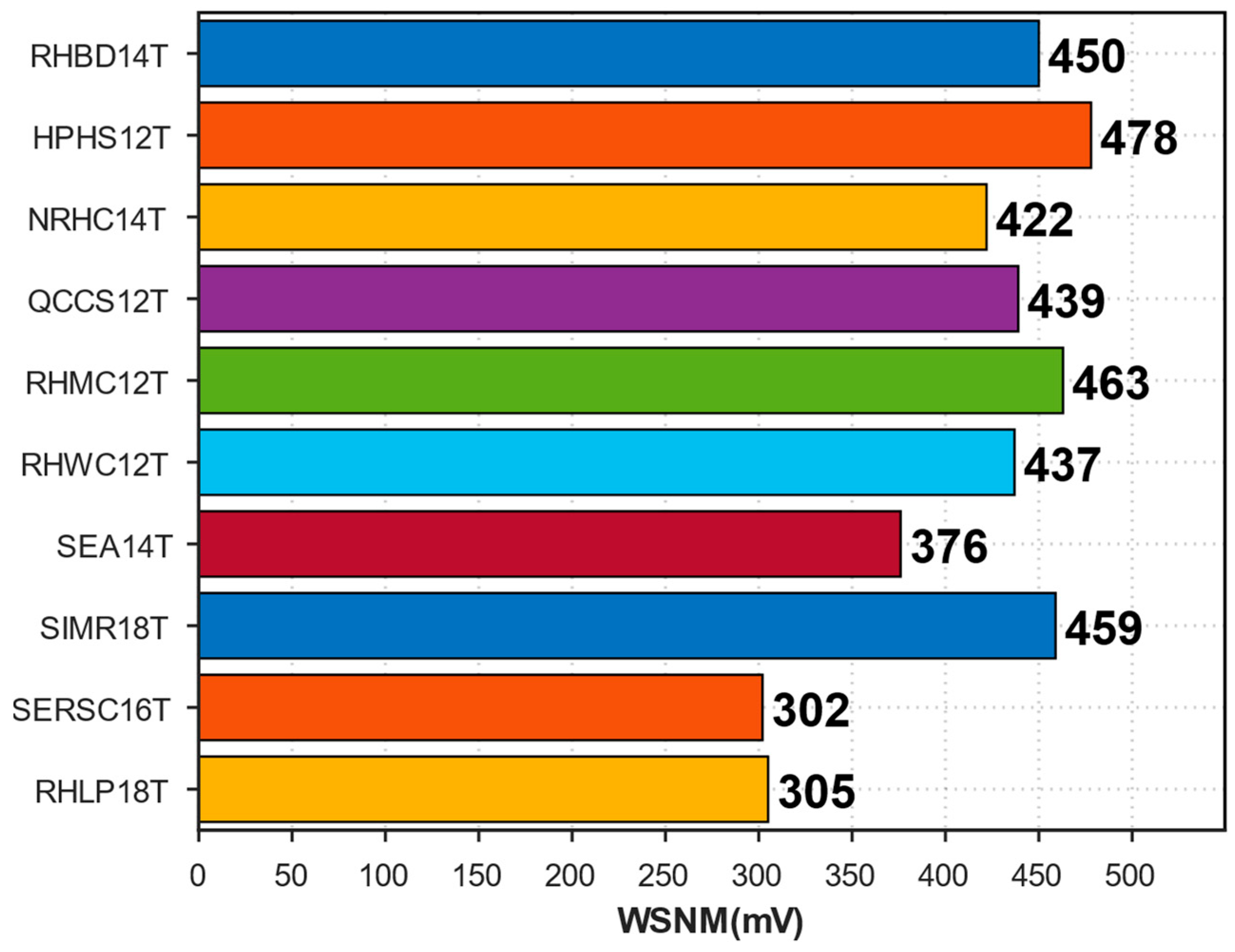
3.1.3. WSNM Comparison

Write Static Noise Margin (WSNM), or Write Margin, measures how easily the cell can be successfully written to with the intended value. It is typically found by analyzing VTCs during the write operation. Similarly to HSNM and RSNM, WSNM is defined as the side length of the largest square that fits between two curves. A higher WSNM generally means better writeability. The proposed RHLP-18T cell has a WSNM of 305 mV (Figure 7). While 305 mV is sufficient for successful writes under normal conditions, it is lower than some competitors like HPHS12T (478 mV) or RHBD14T (450 mV). This suggests that writing to the cell might be easier (potentially faster), but the safety margin against noise during writing is smaller. This is likely a consequence of the effective write-assist mechanism (using WWL and P11/P12), making the lower WSNM a trade-off for potentially better writeability at the expense of write stability margin.

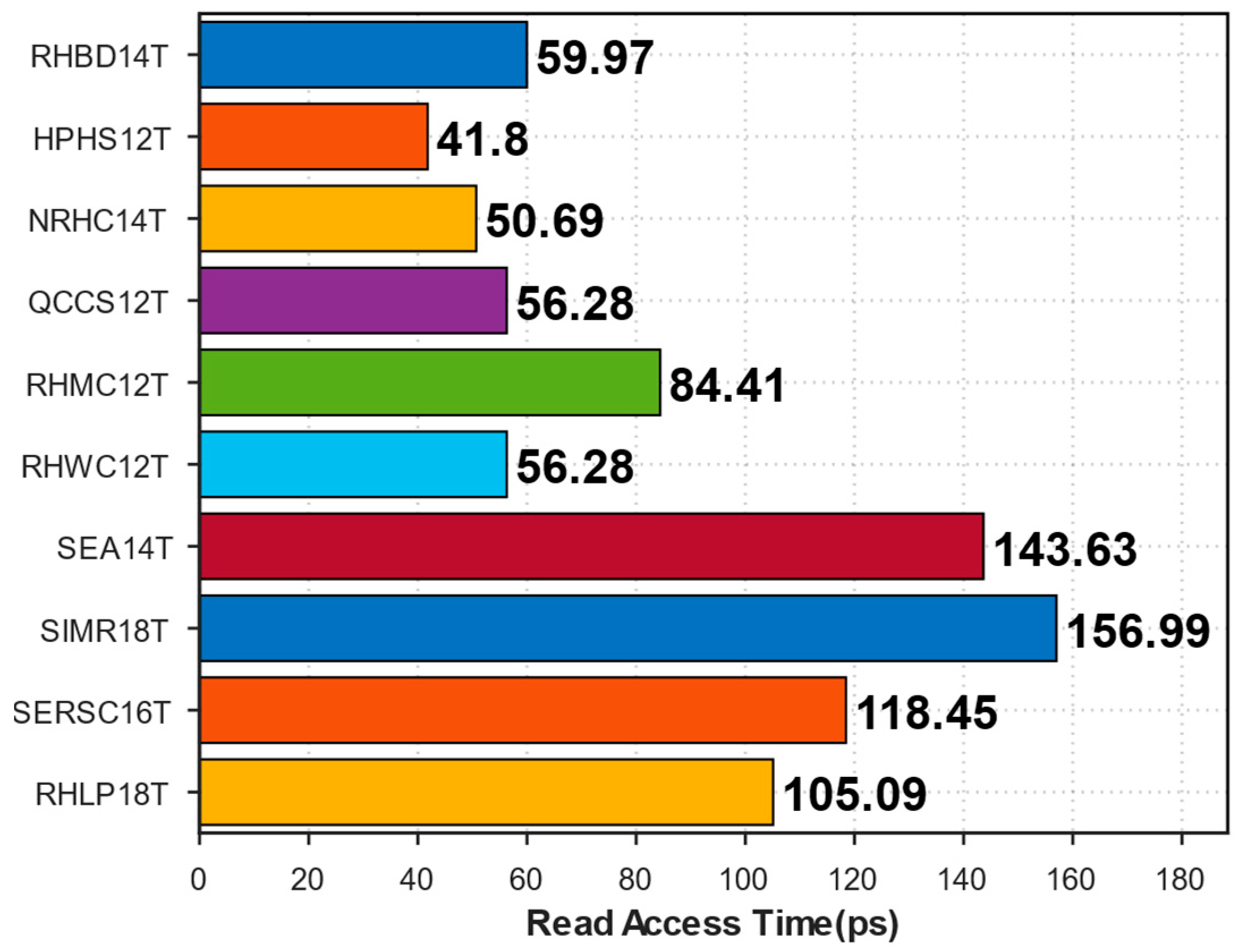
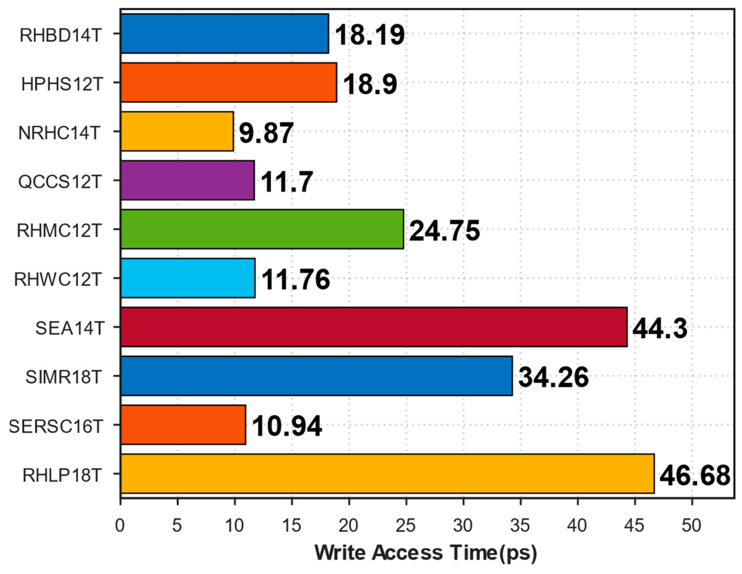
3.2. Access Time Comparison

The Read Access Time (RAT) and the Write Access Time (WAT) indicate how quickly the memory cell operates. RAT is usually the time from WL hitting 50% of VDD until there is a voltage difference of 100 mV (the criterion used for all cell comparisons in this study) between BL and BLB for the sense amplifier to reliably detect the state. WAT is typically the time from WL reaching 50% of VDD until the internal nodes (Q and QB) cross each other’s voltage levels, signifying the state has flipped.
Simulation results (Figure 8 and Figure 9) show that RHLP-18T has a RAT of 105.09 ps and a WAT of 46.68 ps. The RAT is approximately 2.5 times longer than the fastest competitor (HPHS12T at 41.8 ps), and the WAT is approximately 4.6 times longer than the fastest (NRHC14T at 9.87 ps), indicating a significant speed disadvantage. The slower RAT might be attributed to the design approach using WWL to separate read and write paths, potentially combined with limited current drive from the read path transistors (N5, N6). The slower WAT may result from the cell’s relatively long internal feedback loop structure. This reflects a design choice that prioritizes stability, particularly read static noise margin (RSNM), and low power consumption over access speed.

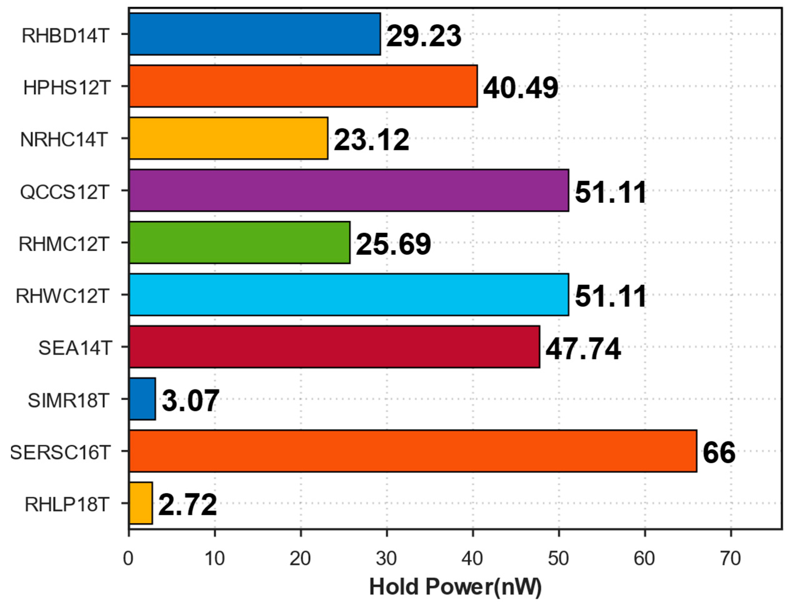
3.3. Hold Power Comparison

Hold power refers to the static power consumed by the SRAM cell when it remains idle while retaining its stored data (‘0’ or ‘1’). This power drain comes mainly from leakage currents (like subthreshold and gate leakage) flowing through the transistors even when they are technically “off”. Since memory arrays often spend most of their time in this standby state, minimizing hold power is vital for energy efficiency, battery life in portable gadgets, and heat management in dense memory chips. In this area, the proposed RHLP-18T performs exceptionally well. It shows the lowest hold power consumption among all compared cells, just 2.72 nW (Figure 10). This is slightly better than the next lowest, SIMR18T (3.07 nW), and much lower than many others like SERSC16T (66 nW) or QCCS12T (51.11 nW). This extremely low static power is likely attributed to the transistor stacking effect inherent in the cell’s 18T structure. By utilizing a larger number of transistors (18T), multiple series-connected “off” transistors are formed within potential leakage paths during the hold mode. This stacking significantly suppresses subthreshold leakage current, a primary contributor to static power. Consequently, the observed low hold power is a significant advantage, making RHLP-18T very attractive for applications where power is limited.

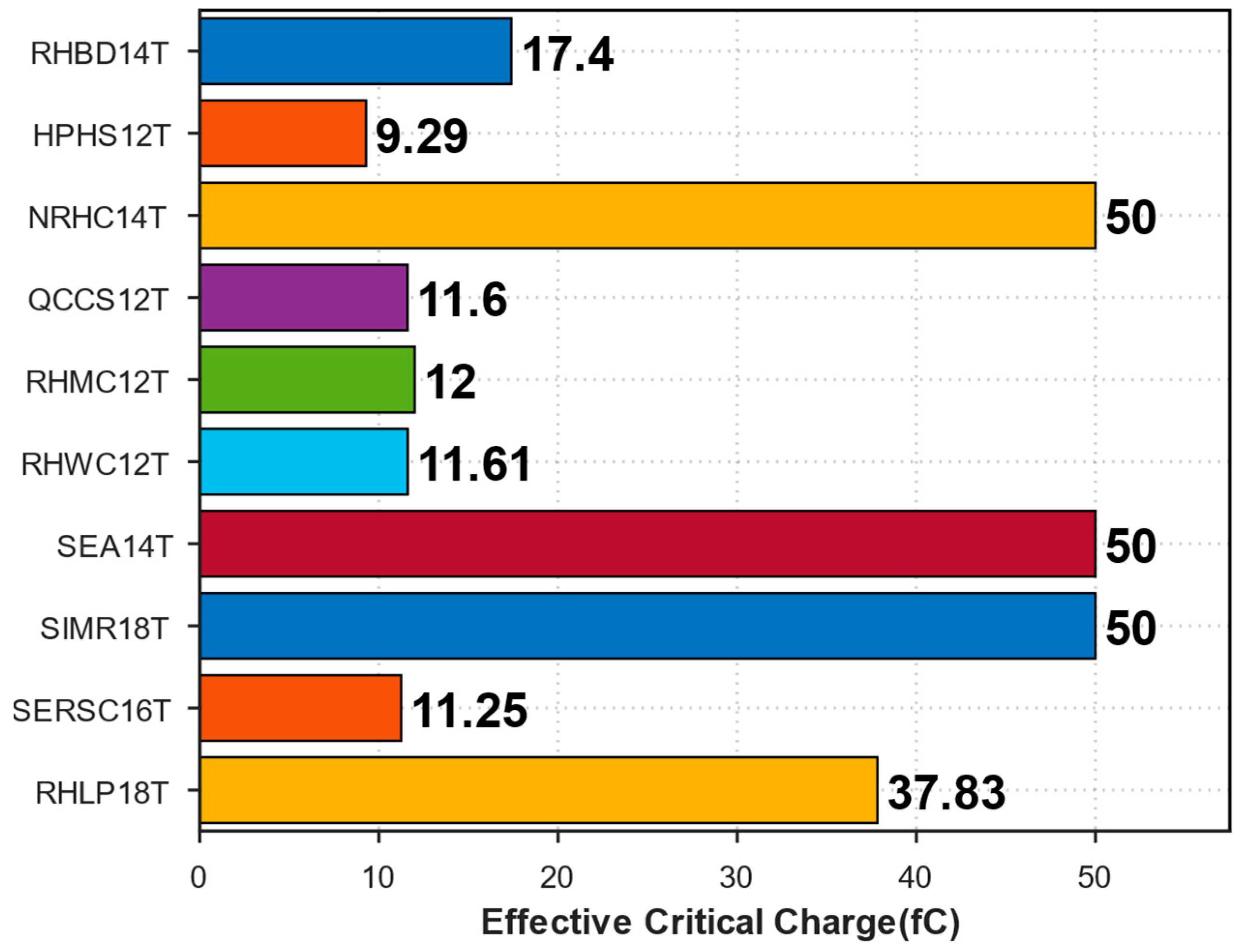
3.4. SEU and SEDNU Robustness Comparison

To evaluate a circuit’s resilience to radiation-induced errors such as SEUs and DNUs, transient fault injection simulations are typically performed. This involves injecting a brief current pulse at sensitive nodes in the circuit model to simulate the charge deposited by a high-energy particle hit [20]. The minimum amount of this injected charge needed to flip the cell’s state is the critical charge (Qc), with higher values indicating greater robustness. Specifically, Qc represents the minimum value of Q i n j found through simulation that successfully induces an upset. The injected current pulse shape, I i n j t , is commonly modeled using a double-exponential function, as shown in Equation (1):
I i n j t = Q i n j τ α τ β e t τ α e t τ β
Here, Q i n j is the total charge injected in a single event simulation; τ α is the charge collection time constant; and τ β relates to the ion track formation time. Based on the relevant literature for this technology node, τ α and τ β were set to 50 ps and 200 ps, respectively [21]. Figure 11 illustrates example transient waveforms resulting from such charge injections at various sensitive nodes. Additionally, the time at which the current pulse reaches its maximum, t m a x can be determined. When τ α is 50 ps and τ β is 200 ps, t m a x is 93 ps, as shown in Equation (2).
t m a x = τ α τ β τ β τ α ln τ β τ α
Proposed RHLP-18T cell achieves a critical charge (Qc) of 37.83 fC (Figure 12). While this is not the absolute highest value reported—NRHC14T, SEA14T, and SIMR18T boast Qc > 50 fC—it is considerably better than many other cells, such as HPHS12T (9.29 fC), QCCS12T (11.6 fC), and RHBD14T (17.4 fC). This demonstrates a solid, competitive level of tolerance against SEUs. As mentioned back in Section 2.2, the cell’s defense against certain SEDNUs relies on careful layout design rather than inherent circuit recovery.

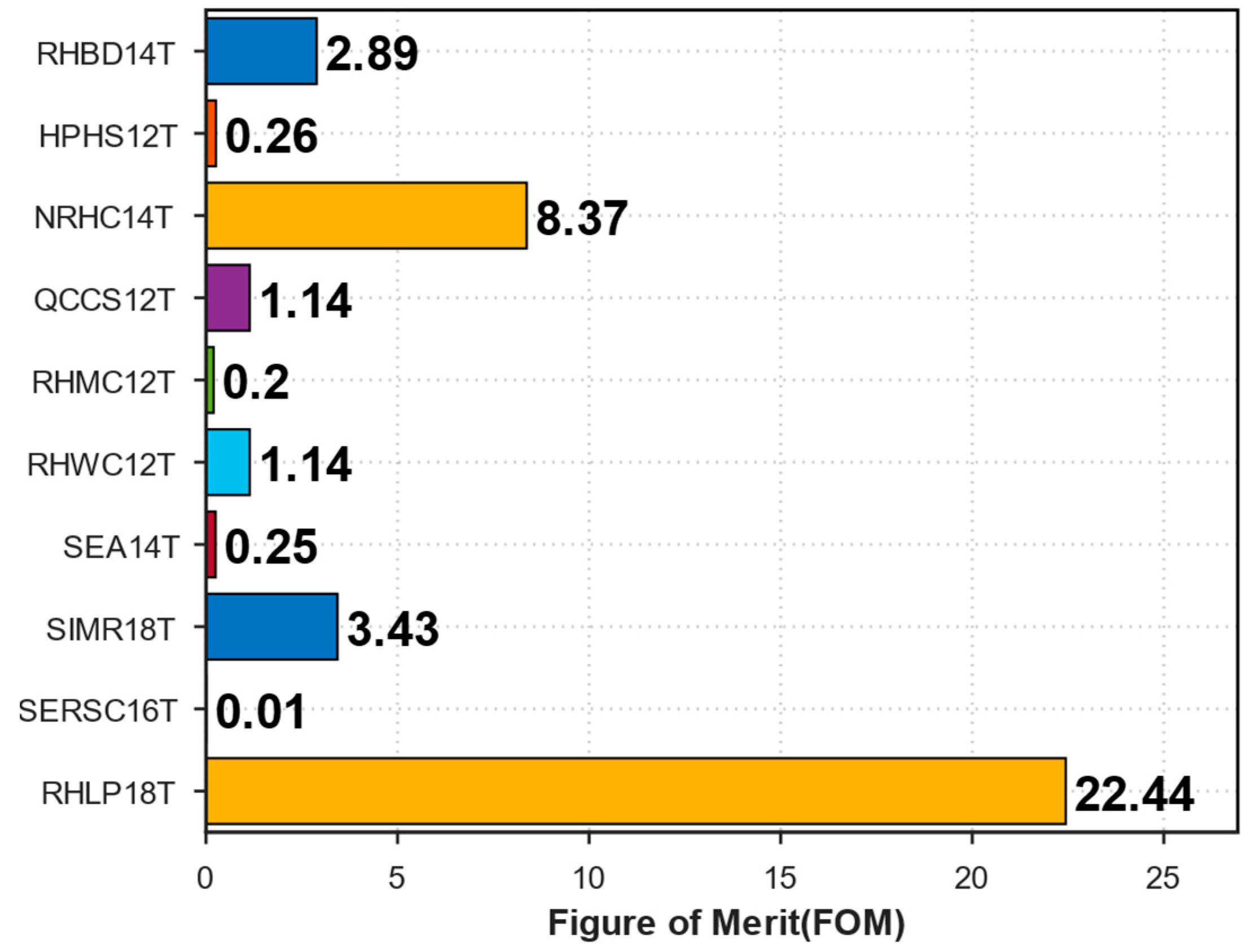
3.5. Figure of Merit (FOM)

Evaluating an SRAM cell requires balancing multiple performance metrics that often exhibit trade-off relationships. To enable a comprehensive comparison that accounts for these trade-offs, a Figure of Merit (FOM) is employed. This FOM integrates key parameters related to stability (HSNM, RSNM, WSNM), effective critical charge (Qc), speed (RAT, WAT), and power consumption (hold power). The specific formula used to compute the FOM in this study, as presented in Equation (3), was adopted with reference to previous works [9,10,11,12,13,14,15,16,17]:
F O M = H S N M × R S N M × W S N M × Q C R A T × W A T × H o l d P o w e r
As shown in Figure 13, the proposed RHLP-18T cell achieves the highest FOM value among all evaluated designs, with a score of 22.44, significantly surpassing the others. This high FOM value underscores the cell’s well-balanced performance, particularly its excellent read stability and low hold power consumption, despite its relatively slower access times. Table 1 presents a performance comparison between the proposed RHLP-18T cell and other existing radiation-hardened SRAM cell architectures.

4. Conclusions

In this paper, RHLP-18T, a radiation-hardened 18-transistor SRAM cell, was presented. The design was developed with the objectives of achieving high read stability, low static power consumption, and robustness against Single Event Upsets. Transient fault simulations were conducted using 90 nm CMOS technology to evaluate its performance in comparison with nine existing Radiation-Hardened-By-Design SRAM cells. The proposed RHLP-18T cell demonstrated superior performance in several key aspects: It achieved the highest Read Static Noise Margin, indicating exceptional read stability, and exhibited the lowest hold power consumption, reflecting high energy efficiency. In addition, it maintained a competitive level of SEU tolerance, as evidenced by its effective critical charge.
These combined strengths enabled RHLP-18T to achieve the highest Figure of Merit among all of the evaluated designs, highlighting its balanced performance characteristics. This result suggests that RHLP-18T is a promising candidate for applications where high reliability and low power consumption are essential, such as in aerospace and spaceborne systems. However, these advantages are accompanied by certain trade-offs. Specifically, RHLP-18T exhibits longer read and write access times, along with a slightly reduced HSNM and WSNM, compared to some alternative designs. These limitations reflect a conscious design decision to prioritize read stability and static power efficiency over high-speed access and write robustness. However, these compromises severely limit its viability in high-speed memory applications, presenting a major obstacle that requires targeted design improvements.

Author Contributions

Conceptualization, H.-G.K. and S.-H.J.; methodology, H.-G.K.; validation, H.-G.K.; data curation, H.-G.K.; writing—original draft preparation, H.-G.K.; writing—review and editing, S.-H.J.; visualization, H.-G.K.; supervision, S.-H.J.; project administration, S.-H.J. All authors have read and agreed to the published version of the manuscript.

Funding

This research received no external funding.

Institutional Review Board Statement

Not applicable.

Informed Consent Statement

Not applicable.

Data Availability Statement

Data are contained within the article.

Acknowledgments

The EDA Tool was supported by the IC Design Education Center, Republic of Korea.

Conflicts of Interest

The authors declare no conflicts of interest.

References

  1. Holmes-Siedle, A.; Adams, L. Handbook of Radiation Effects; Oxford University Press: Oxford, UK, 2002; ISBN 978-0-19-850733-8. [Google Scholar]
  2. Pasupathy, K.R.; Bindu, B. Analysis of Bipolar Amplification Due to Heavy-Ion Irradiation in 45 Nm FDSOI MOSFET with Thin BOX and Ground Plane. Microelectron. Reliab. 2019, 98, 56–62. [Google Scholar] [CrossRef]
  3. Pal, S.; Ki, W.-H.; Tsui, C.-Y. Soft-Error-Aware Read-Stability-Enhanced Low-Power 12T SRAM with Multi-Node Upset Recoverability for Aerospace Applications. IEEE Trans. Circuits Syst. I 2022, 69, 1560–1570. [Google Scholar] [CrossRef]
  4. Dodd, P.E.; Massengill, L.W. Basic Mechanisms and Modeling of Single-Event Upset in Digital Microelectronics. IEEE Trans. Nucl. Sci. 2003, 50, 583–602. [Google Scholar] [CrossRef]
  5. Dohar, S.S.; Siddharth, R.K.; Vasantha, M.H.; Nithin Kumar, Y.B. A 1.2 V, Highly Reliable RHBD 10T SRAM Cell for Aerospace Application. IEEE Trans. Electron Devices 2021, 68, 2265–2270. [Google Scholar] [CrossRef]
  6. Huang, Q. Investigation of Radiation-Hardened Design of Electronic Systems with Applications to Post-Accident Monitoring for Nuclear Power Plants. Ph.D. Thesis, The University of Western Ontario, London, ON, Canada, 2019. [Google Scholar]
  7. Cai, S.; Liang, X.; Wen, Y.; Yu, F.; Yin, L. A Radiation-Hardened 20T SRAM Cell with High Reliability and Low Power Consumption. In Proceedings of the 2024 IEEE International Test Conference in Asia (ITC-Asia), Changsha, China, 18 August 2024. [Google Scholar]
  8. Aguiar, Y.Q.D.; Wrobel, F.; Autran, J.-L.; García Alía, R. Single-Event Effects, from Space to Accelerator Environments: Analysis, Prediction and Hardening by Design; Springer International Publishing: Cham, Switzerland, 2025; ISBN 978-3-031-71722-2. [Google Scholar]
  9. Kiamehr, S.; Osiecki, T.; Tahoori, M.; Nassif, S. Radiation-Induced Soft Error Analysis of SRAMs in SOI FinFET Technology: A Device to Circuit Approach. In Proceedings of the 51st Annual Design Automation Conference, San Francisco, CA, USA, 1–5 June 2014. [Google Scholar]
  10. Prasad, G.; Mandi, B.C.; Ali, M. Energy-Efficient Radiation Hardened SRAM Cell for Low Voltage Terrestrial Applications. Microelectron. J. 2022, 120, 105340. [Google Scholar] [CrossRef]
  11. Mukku, P.K.; Lorenzo, R. An Efficient Radiation Hardening SRAM Cell to Mitigate Single and Double Node Upset Soft Errors. Microelectron. Reliab. 2024, 152, 115303. [Google Scholar] [CrossRef]
  12. Hao, L.; Liu, L.; Shi, Q.; Qiang, B.; Li, Z.; Liu, N.; Dai, C.; Zhao, Q.; Peng, C.; Lu, W.; et al. Design of Radiation-Hardened Memory Cell by Polar Design for Space Applications. Microelectron. J. 2023, 132, 105691. [Google Scholar] [CrossRef]
  13. Kumar, S.; Mukherjee, A. Design of Soft-Error Resilient SRAM Cell with High Read and Write Stability for Robust Operations. AEU Int. J. Electron. Commun. 2023, 168, 154719. [Google Scholar] [CrossRef]
  14. Pal, S.; Mohapatra, S.; Ki, W.-H.; Islam, A. Design of Soft-Error-Aware SRAM with Multi-Node Upset Recovery for Aerospace Applications. IEEE Trans. Circuits Syst. I 2021, 68, 2470–2480. [Google Scholar] [CrossRef]
  15. Liu, Z.; Zhang, H.; Xie, Y.; Bi, D.; Hu, Z.; Zou, S.; Zhang, Z. High-Performance and Highly-Stable Soft Error Resistant 12T SRAM Cell for Space Applications. Microelectron. Reliab. 2023, 141, 114885. [Google Scholar] [CrossRef]
  16. Bai, N.; Zhou, Y.; Xu, Y.; Wang, Y.; Chen, Z. Highly Stable Soft-Error Immune SRAM with Multi-Node Upset Recovery for Aerospace Applications. Integration 2023, 92, 58–65. [Google Scholar] [CrossRef]
  17. Zhao, Q.; Dong, H.; Wang, X.; Hao, L.; Peng, C.; Lin, Z.; Wu, X. Novel Radiation-Hardened SRAM for Immune Soft-Error in Space-Radiation Environments. Microelectron. Reliab. 2023, 140, 114862. [Google Scholar] [CrossRef]
  18. Yan, A.; Xiang, J.; Cao, A.; He, Z.; Cui, J.; Ni, T.; Huang, Z.; Wen, X.; Girard, P. Quadruple and Sextuple Cross-Coupled SRAM Cell Designs with Optimized Overhead for Reliable Applications. IEEE Trans. Device Mater. Relib. 2022, 22, 282–295. [Google Scholar] [CrossRef]
  19. Sharma, R.; Mondal, D.; Shah, A.P. Radiation Hardened 12T SRAM Cell with Improved Writing Capability for Space Applications. Mem. Mater. Devices Circuits Syst. 2023, 5, 100071. [Google Scholar] [CrossRef]
  20. Li, H.; Xiao, L.; Qi, C.; Li, J. Design of High-Reliability Memory Cell to Mitigate Single Event Multiple Node Upsets. IEEE Trans. Circuits Syst. I 2021, 68, 4170–4181. [Google Scholar] [CrossRef]
  21. Kumar, S.; Mukherjee, A. High Performance Radiation-Hardened SRAM Cell Design for Robust Applications. Microelectron. J. 2023, 140, 105934. [Google Scholar] [CrossRef]
Figure 1. Schematic of the proposed RHLP-18T cell.
Applsci 15 05712 g001
Figure 2. Layout of proposed RHLP-18T cell.
Applsci 15 05712 g002
Figure 3. Waveforms of the memory operation of proposed RHLP-18T cell.
Applsci 15 05712 g003
Figure 4. Waveforms of SEU and SEDNU recovery of the proposed RHLP-18T cell.
Applsci 15 05712 g004
Figure 5. HSNM comparison between the proposed RHLP-18T cell and previous works.
Applsci 15 05712 g005
Figure 6. RSNM comparison between the proposed RHLP-18T cell and previous works.
Applsci 15 05712 g006
Figure 7. WSNM comparison between the proposed RHLP-18T cell and previous works.
Applsci 15 05712 g007
Figure 8. Read Access Time comparison between the proposed RHLP-18T cell and previous works.
Applsci 15 05712 g008
Figure 9. Write Access Time comparison between the proposed RHLP-18T cell and previous works.
Applsci 15 05712 g009
Figure 10. Hold power access time comparison between the proposed RHLP-18T cell and previous works.
Applsci 15 05712 g010
Figure 11. Different amounts of charge (10 to 35 fC) are injected into (a) node Q (b) node QB (c) node S1, and (d) 10 to 25 fC is injected into nodes Q and QB simultaneously.
Applsci 15 05712 g011
Figure 12. Critical charge comparison between the proposed RHLP-18T cell and previous works.
Applsci 15 05712 g012
Figure 13. Comparison of Figures of Merit (FOM).
Applsci 15 05712 g013
Table 1. Performance comparison between the RHLP-18T cell and other radiation-hardened SRAM cell structures.
Structure NameHSNM
/mV
RSNM
/mV
WSNM
/mV
Qc
/fC
RAT
/ps
WAT
/ps
Hold Power
/nW
FOM
RHBD-14T2404945017.459.9718.1929.232.89
HPHS-12T173114789.2941.818.940.490.26
NRHC-14T15330422>5050.699.8723.128.37
QCCS-12T2782743911.656.2811.751.111.14
RHMC-12T196104631284.4124.7525.690.2
RHWC-12T2812743711.6156.2811.7651.111.14
SEA-14T22218376>50143.6344.347.740.25
SIMR-18T13718459>50156.9934.263.073.43
SERSC-16T211130211.25118.4510.94660.01
This work17315030537.83105.0946.682.7222.44
Disclaimer/Publisher’s Note: The statements, opinions and data contained in all publications are solely those of the individual author(s) and contributor(s) and not of MDPI and/or the editor(s). MDPI and/or the editor(s) disclaim responsibility for any injury to people or property resulting from any ideas, methods, instructions or products referred to in the content.

