Featured Application
The presented results can be useful for engineers working on the reliability of the soldering process.
Abstract
In this paper, the issue of an aging process’s influence on power LEDs’ properties is considered. Some measured DC characteristics of these devices and their thermal and optical parameters obtained are presented after considering different values of the aging process’ duration. Components soldered using different metal–ceramic composite pastes, e.g., with TiO2, were tested. The tested devices and the used measurement setup are described. The measurement procedure is described in detail. The obtained measurement results are discussed. It is shown that after the aging process at elevated temperatures, worse properties were observed for the power LEDs soldered using classical SACX0307 alloy. Most of the samples soldered with reference alloy (not composite) were damaged during the test. The best properties were obtained for the samples soldered with solder paste with the addition of titanium oxide.
1. Introduction
In recent years, a speedy development in the lighting technique was observed due to the use of solid-state light sources [1]. The essential components of these sources are power LEDs (Light-Emitting Diodes) [1,2,3], which convert electrical energy into light. During the operation of these devices, some part of the electrical energy is also converted into heat [3]. This phenomenon causes an increase in the junction temperature of the diodes, causing self-heating [3,4,5,6]. The junction temperature increase causes a decrease in the luminous flux of the emitted light and a reduction in the luminous efficacy (ηE) [7,8]. As it was shown in [9], at very high junction temperatures exceeding 120 °C, the value of ηE can decrease several times
All electronic components, including power LEDs, are sensitive to aging [10]. These processes result in changes in the operational parameters and ultimately lead to their damage [11]. Sensitivity to aging processes depends on many factors and, above all, on their junction temperature Tj [10,11]. This temperature is a sum of the ambient temperature Ta and an increase in temperature caused by self-heating phenomena. This increase is a product of the power dissipated Pth and the thermal resistance characterizing the efficiency of heat removal [12,13,14]. The thermal resistance Rth is defined by the following formula [15,16]:
Thermal resistance Rth depends on the heat flow path. This path consists of the following components: semiconductor chip, thermal interfaces, and the substrate and housing of the tested power LED [17]. The soldering profile used, the type of soldering oven, and the size of the printed circuit board (PCB) have a significant impact on the value of thermal resistance Rth [18,19,20,21]. Soldering parameters substantially influence the electronic devices’ electrical, thermal, and optical parameters.
Results of the mechanical properties of solder joints fabricated using SAC305, Sn62Pb36Ag2, and Sn60Pb40 solder pastes are reported in Refs. [22,23]. The experimental results showed that the thickness of intermetallic layers increases with an increased soldering alloy liquidus temperature. In the paper of H. Gopalakrishna [22], the results of experimental studies on the mechanical properties of soldered joints used in solar cells present that the operation time in elevated environmental conditions is about 20 years. It is proven that the use of Ag in the soldering alloy affects the mitigation of the solder binder degradation.
M. S. Alam et al. described [23] the results of experimental studies on thermal cycles during the deformation of solder joints at eight different temperatures ranging from 25 to 200 °C. In paper [24], statistical methods dedicated to analyses of thermal cycles in power supply systems and power semiconductor devices are considered, and an algorithm for lifetime prediction is proposed.
In the paper of Górecki et al. [25], the results of experimental studies illustrating the influence of the soldering process on thermal parameters of transistors operating in RF (Radio Frequency) systems are presented. It was also proven that the thermal resistance Rth and the dissipated power change the lifetime of tested transistors.
Results of the influence of thermal phenomena of multi-colored power LEDs on thermal resistance and the normalized value of the emitted optical power are reported in [26,27]. Various degradation mechanisms of the tested power LEDs are also identified using X-ray images of solder joints after a specified aging test period. In paper [27], the influence of temperature, current shocks, and blue light stimulation on the degradation process of the applied luminophore used in power LEDs was also analyzed.
In the paper of Peng et al. [28], the results of experimental studies on the aging of high-power white LEDs are presented, with the most significant emphasis on tests of the optical components of the tested LED chips, i.e., lenses and phosphors. An apparent decrease in the optical power emitted by the tested chips was observed in all three tested LED chips. At the same time, the thermal properties and angles of maximum light intensity did not change after the aging process.
Baba et al. [29] brought an overview of APC (Active Power Cycling) tests of SiC (silicon carbide) half-bridge modules. This description covers all aspects of accelerated aging tests, from the preparation of the APC test to the post-failure analysis of SiC half-bridge modules, ending with identifying their reliability model. Moreover, the tested SiC modules were subjected to special 14-week tests after the aging process to determine the further degradation of electrical parameters.
In the paper of Hegedus et al. [30], different aging models of white power LEDs were analyzed, which improved their multi-domain model with a component describing the influence of lifetime on selected parameters of the tested devices. The authors of the cited paper take an approach based on the LM-80-08 testing method [31], supplemented with additional specific thermal measurements of white power LEDs.
The power semiconductor devices operate not only in ideal environmental conditions but also in elevated temperatures and relative humidity, often reaching 100%. The results of aging tests of white power LEDs and RGB power LEDs in such unfavorable environmental conditions were presented in the work of Harsanyi et al. [32]. It was found that the influence of the humidity (85%) is much more considerable than expected, and the power LEDs show very different behaviors in terms of their operating parameters, such as forward voltage, electrical power, emitted optical power, energy conversion efficiency, thermal resistance, total luminous flux, and CCT. The material from which the luminophore is made extensively impacts aging processes activated by environmental conditions. It can be seen that RGB power LEDs show a more negligible dependence on the degradation of optical parameters than white power LEDs, whose luminophore contains large amounts of luminophore used to convert blue light into white light with different correlated color temperature (CCT). Large amounts of phosphorus in the luminophore cause more significant absorption of water molecules from the atmosphere. It was also proven that water molecules penetrating the lower luminophore layers in white power LEDs with a high CCT (Cold White) lead to the degradation of the lower phosphor layers and cause the degradation of thermal interfaces under the LED chip, which leads to the deterioration of thermal and optical parameters of the tested power LEDs.
The aging test results of white LEDs with a power dissipation of 1 W, excited with direct current, and a half-wave rectified sinusoidal waveform were presented by Juarez et al. [33]. The aging tests lasted 6500 h at a temperature of 85 °C. It was reported that supplying power LEDs with direct current has a negligible effect on their lifetime (exceeding 50,000 h), while supplying with a half-wave rectified sine current drastically reduces their lifetime—to about 7000 h—and damages the luminophore manifesting by blue light emission.
Currently, in soldering alloys, TiO2 is used the most frequently as a reinforcement material [34,35]. The enhanced metallurgical properties (toughness, ductility, and yield strength) of soldering alloys can be obtained as a result of grain refinement [34]. On the other hand, the reinforcement addition could change many important properties of solder joints. For example, it can cause surface instability [36], the grain boundary/interfacial characteristics and the variation in the physical properties [36,37]. For the classical SAC alloy, the solder joints contain a β–Sn matrix and Intermetallic Compounds (IMCs). As IMCs, Cu3Sn, Cu6Sn5, and Ag3Sn are usually observed [38].
As it was mentioned in [37], the particles of TiO2 can influence many parameters of the soldering alloy. It is essential that the addition of TiO2 changes the IMC growth. It causes a decrease in the thickness of the IMC layer [38]. However, it changes the size of the Ag3Sn grains and the spacing between them [34,39]. The reduction in this spacing causes a substantial increase in the material microhardness [34].
This paper aims to present the influence of the soldering alloy composition used for power LED assembly and the duration of the aging process on their electrical characteristics, as well as optical and thermal parameters. The tested soldering alloy contains reinforcements of TiO2 characterized by different sizes of particles. The characteristics of the tested LEDs were measured after different values of aging time in the elevated temperature. It is proved that using modified soldering alloy makes it possible to obtain a longer lifetime than the classical SACX0307 soldering alloy.
2. Investigated LED and Soldering Process
Tests were carried out for power LEDs of the XMLBWT-02-0000-000HT20E7 type produced by Wolfspeed Inc. [40] (Durham, NC, USA). The LEDs were used with a maximum admissible forward current IFmax = 3 A and a maximum admissible junction temperature Tjmax = 150 °C. Thermal resistance between the junction of this LED and the soldering point was Rthj-s = 2.5 K/W [40]. The diode was characterized by its correlated color temperature CCT = 3000 K. In contrast, the generated luminous flux is equal to Φv = 200 lm at the forward current IF = 700 mA and junction temperature Tj = 85 °C.
The tested devices were soldered to MCPCB (Metal Core Printed Circuit Board) of the type XM-NT-1SB22-F [41]. In the soldering process, three types of solder pastes were used: the classical SACX0307 alloy (REF) and composite ones, SACX-TiO2 (containing grains of TiO2 of a diameter of 200 nm) and SACX-TiO2 nano (containing grains of TiO2 of a diameter of 20 nm).
In the soldering process of the samples, a convection reflow oven SMT 460C (Essemtec AG, Aesch, Switzerland) was used. The temperature profile of the soldering process is presented in Figure 1. The linear temperature profile contains 3 phases: pre-heating (duration equal to 60 s, temperature range of 160–180 °C), reflowing (duration equal to 40 s, temperature range of 213–247 °C), and cooling (duration equal to 70 s, temperature decreases from 247 °C to 150 °C). The convection reflow was performed in an air atmosphere.
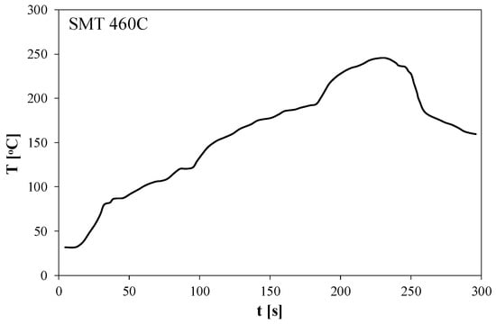
Figure 1.
Temperature profile of convection reflow oven SMT 460C.
The tested LEDs were assembled using each of the mentioned solder pastes. Three of the tested LEDs were assembled in each group with each kind of tested paste. Alumina substrates, Star MCPCB board with a 22 mm diameter and 2.4 mm thickness, were used. A Cu layer covered these substrates with a 60 µm thickness. The galvanic Ni/Au layer with a 2.5/0.25 µm thickness was used as a surface finish [41].
During the test, the LEDs mounted on the MCPCB were situated on the alumina heat sink. A view of the sample is shown in Figure 2a, and samples assembled for the test are shown in Figure 2b. The dimensions of the used heat sink were as follows: 250 × 125 × 35 mm.
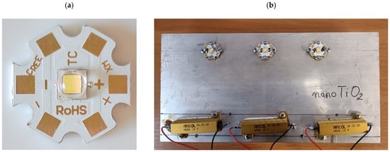
Figure 2.
LED mounted on MCPCB (a) and assembled on heat sink (b).
Composite soldering alloys were made based on SACX0307 (Sn99Ag0.3Cu0.7) solder paste produced by Alpha Industries (Chantilly, VA, USA). To this paste, 1.0 wt. % of TiO2 reinforcements produced by Sigma-Aldrich (St. Louis, MI, USA) were added. These reinforcements have two sizes: 20 nm (nanoparticles) and 200 nm (submicron particles). The paste and reinforcements were mixed homogeneously using the ball milling process. This process was carried out using a planetary ball mill Pulverisette 5 produced by Fritsch GmbH (Idar-Oberstein, Germany) for 10 min at 300 rpm.
The solder paste SACX0307 without any reinforcements was used as the reference sample. Stencil printing with a stencil thickness of 125 µm was used to prepare the solder joints. The stencil aperture was narrowed by 10% over the thermal pad to avoid a shortcut during the soldering process (Figure 3).
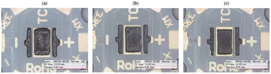
Figure 3.
Solder paste stencil for SACX0307-REF (a), SACX0307-nanoTiO2 (b), and SACX0307-TiO2 (c).
3. Measurement Method and Setup
The aging process of all the tested devices was performed simultaneously using a dedicated environmental chamber. During the aging process, LEDs operated at the rated value of their forward current IF = 3 A at an ambient temperature of 80 °C. This ambient temperature was selected to make the aging process faster. According to the Arrhenius equation [42], an increase in temperature value equal to 55 °C causes over a 60-fold reduction in the lifetime of tested devices. This means that operation at a temperature of 80 °C for 1000 h corresponds to operation at a temperature of 25 °C for 60,000 h. During the test the humidity value was not registered. The aging process is carried out in the following mode:
- Step 1: The operation of the tested diodes in the above-described conditions for a predetermined time.
- Step 2: The measurement of the electrical, optical, and thermal parameters of the diodes under study.
Steps 1 and 2 are performed alternately until the end of the test.
The quasi-isothermal I-V characteristics, thermal resistance Rth, and luminous flux ΦV before the start of the heating cycle (t = 0) and after time intervals equal to 100 h, 250 h, 500 h, and 1000 h were measured.
A measurement setup like that in the diagram shown in Figure 4 makes it possible to measure thermal resistance, the DC current–voltage characteristics, and illuminance of the LEDs. The measurements were performed for the samples mounted onto an aluminum heat sink (Figure 2b) and situated in a light-tight chamber. The papers by Poppe, A., and Skwarek, A. [9,43], provide a detailed description of the measurement method for thermal and optical parameters.
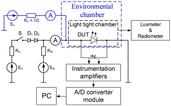
Figure 4.
Measurement setup of the LED test system.
In Figure 4, the blue color indicates the part of the power supply system of the tested LED during its aging in the environmental chamber. In turn, the black color indicates the part of the system used for measuring electrical, optical, and thermal parameters.
During the aging process, a current of a fixed value regulated by a voltage source EA flows through the tested LED, and the environmental chamber provides the fixed value of the ambient temperature. The value of this current is limited by the resistor RA and measured with an ammeter. The limitation of the value of the diode forward current protects the tested devices against electrical damage, but it cannot protect these devices against thermal damage during the test.
During the measurement of current–voltage characteristics, switch S is open, the voltage on the voltage source EM increases linearly, and the system consisting of instrumentation amplifiers, an A/D converter module, and a computer records the voltage values on the diode and the corresponding current values of this device. In turn, the thermal parameter (thermal resistance Rth) is measured using the indirect electrical method described, among others, in [6]. In this method, it is necessary to switch the diode current from the heating supply (closed switch S) to the measuring supply (open switch S) and measure the diode forward voltage VH immediately after opening the switch S, which preceded obtaining the thermally steady state in the tested diode. Based on the previously measured thermometric characteristic VF(T), the measured voltage VH, and the value of power dissipated in the diode before opening the switch S, the value of thermal resistance Rth is determined.
At the heating supply, the value of the diode forward current is determined by voltage source EH and the resistor RH, whereas the diode forward current at the measuring supply is determined by the voltage source EM and the resistor RM. Diodes D1 and D2 protect the voltage source EH against reverse polarization during the measurements of Rth. During this measurement, the illuminance and optical power density values are also measured using a luxmeter and a radiometer. Based on the results of these measurements, the luminous flux ΦV and optical power Popt are determined using the method described in [44].
4. Results
The results of the performed investigations are shown in Figure 5, Figure 6, Figure 7, Figure 8, Figure 9, Figure 10, Figure 11 and Figure 12. In these figures, individual samples are marked with a number from 1 to 9. The soldering alloy is given in brackets according to the following code: REF—SACX0307 alloy; TiO2—SACX0307 alloy with an addition of TiO2 (200 nm); and nanoTiO2—SACX0307 (20 nm) alloy with an addition of TiO2 nanopowder. During the measurements, some of the tested LEDs were damaged. A photo presenting all samples after the accelerated aging test is shown in Figure 5.
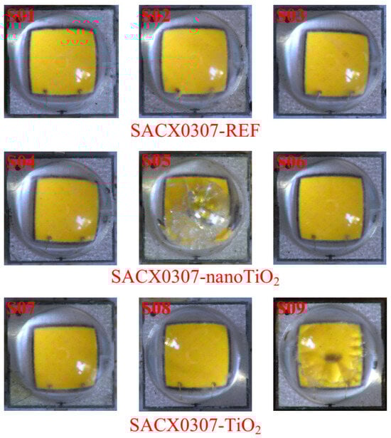
Figure 5.
Views of lens and chips of tested LEDs after aging test.
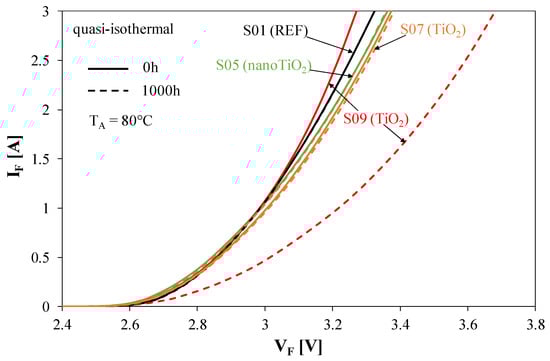
Figure 6.
I-V characteristics of tested devices obtained at t = 0 (solid lines) and at t = 1000 h (dashed lines).
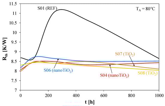
Figure 7.
Thermal resistance of LEDs during the aging process.
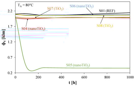
Figure 8.
Luminous flux changes in LEDs during the aging process.
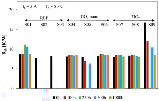
Figure 9.
Thermal resistance changes in LEDs during the aging process.
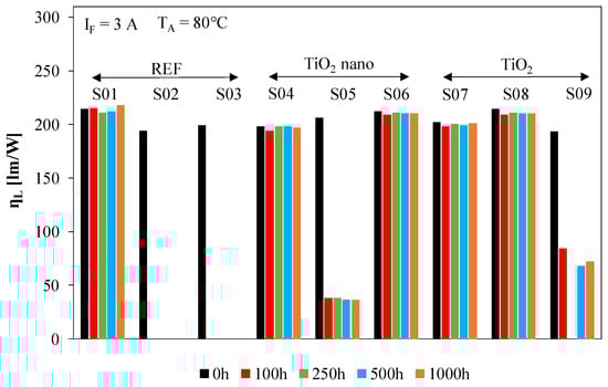
Figure 10.
Luminous efficacy LEDs during the aging process.
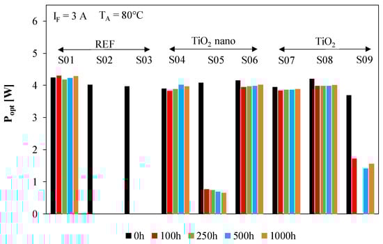
Figure 11.
Optical power of LEDs during the aging process.
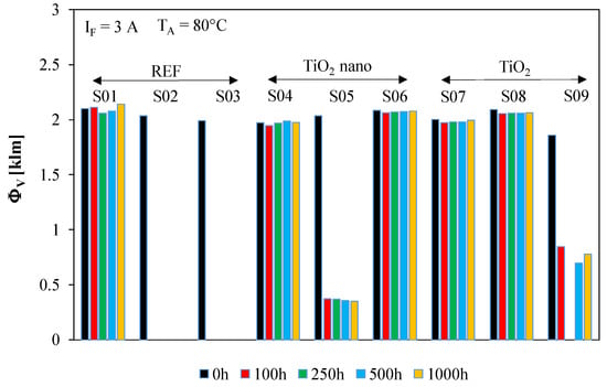
Figure 12.
Luminous flux of LEDs during the aging process.
It can be seen in Figure 5 that after the accelerated aging test [45,46], the lenses in samples S05 (SACX0307-nanoTiO2) and S09 (SACX0307-TiO2) were damaged. This damage caused a decrease in the obtained optical parameters of the tested power LEDs. It should also be noted that samples S02, S03, S04, S06, and S08 were damaged due to fatigue of the soldered joint, which caused a lack of current flow through the tested power LED. It can be emphasized that after 1000 h, only four out of nine samples were electrically efficient (S01, S05, S07, S09).
Figure 6 shows the I-V characteristics of the tested LEDs. The solid lines indicate the characteristics measured for the time t = 0 (before starting the aging process), and the dashed lines indicate the characteristics measured for the time t = 1000 h (at the end of the aging test).
As can be seen, some LEDs were damaged before the end of the tests, and characteristics for these LEDs after the 1000 h aging test were unavailable. For many of the tested diodes, there are no visible differences between the characteristics measured before the aging test and after it. Diode S09 recorded the most significant changes in its characteristics. At forward current IF = 3 A, the forward voltage increased beyond 0.4 V after the aging test. In contrast, for diode S07, such changes do not exceed 10 mV. The observed differences between the characteristics of diodes S07 and S09 assembled with the use of the same soldering alloy suggest that individual properties of the tested devices can influence the speed of the degradation of their electrical properties.
Figure 7 illustrates the effect of the aging test duration on the thermal resistance of the LEDs. Significant changes in Rth, up to 25%, were observed for diode S01. After completing the tests, the lowest Rth value was obtained for the diode soldered with an alloy with the addition of TiO2 and the highest for the diode soldered with the reference alloy. A similar shape of the considered dependence is observed for diodes S06 and S08, but the changes in the value of Rth do not exceed 6%.
Figure 8 shows the impact of aging on the luminous flux (ΦV) emitted by individual diodes. For most LEDs, the during of the aging process did not significantly affect the luminous flux. Only for diode S05 is a significant drop (even by 75%) of ΦV visible. It results from damage to the diode lens during heating.
Figure 9 illustrates the effect of the aging test duration on the thermal resistance of the LEDs.
Significant changes in Rth, up to 25%, were observed for diode S01. After completing the tests, it is also visible that the lowest Rth value was obtained for the diode soldered with an alloy with the addition of TiO2, and the highest for the diode soldered with the reference alloy. It is worth noticing that diodes S02 and S03 soldered with the reference alloy were damaged quickly—before 100 h. Similarly, diode S05 was destroyed during the test. For diode S09, the Rth value was almost doubled. For diodes S04, S06, S07, and S08, the Rth changed no more than by a few percentages.
Figure 10 shows the impact of aging on the luminous efficacy (ηL) emitted by individual diodes. Luminous efficacy is a measure of how well a light source produces visible light. It is the ratio of luminous flux to electrical power [42]. The duration the aging process (up to 1000 h) did not significantly affect the luminous efficacy value for most LEDs. Only for diodes S05 and S09 is a significant drop in the ηL value visible, an even 80%. This drop results from damage to the diode lens during heating. It is also worth noting that the most minor changes in the value of ηL during aging are observed for diode S06.
Figure 11 shows the measured optical power values for diodes under test during the aging process.
It is visible that the most significant value of optical power is obtained before the aging process (at t = 0). The optical power slowly increases for diodes that were not damaged during the aging process. The observed changes in the value of this parameter do not exceed 2%.
Figure 12 shows the measured luminous flux values for diodes under test during the aging process.
It is visible that the most significant value of luminous flux is obtained before the aging process (at t = 0). The luminous flux slowly increases for diodes that were not damaged during the aging process. The observed changes in the value of this parameter do not exceed a few percentages. For tested devices S05 and S09, a significant decrease in the value of ΦV for time t > 0 was observed. This decrease is a result of the thermal degradation of the lens of the mentioned LEDs.
Figure 13 shows the transient thermal impedance curves of chosen diodes under test.
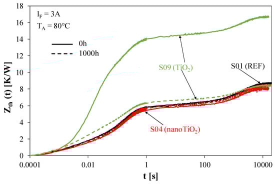
Figure 13.
Waveforms of the transient thermal impedance of LEDs during the aging process.
After 1000 h of the aging test, the differences between the Zth(t) values do not exceed 0.2 K/W. In turn, for the diode marked with symbol S09, a two-fold change in the Zth(t) value is visible. After 1000 h of operation, there is a significant improvement in the efficiency of dissipating the heat generated in this diode. This is probably due to the improved quality of the soldered joint during the aging test.
5. Conclusions
The research results presented in this paper indicate that aging processes occur with different intensities depending on the soldering alloy used. Diodes soldered with the classic SACX0307 alloy were damaged most quickly. Most diodes soldered with this alloy failed before testing was completed, and some were damaged after 100 h of the test.
For diodes soldered using an alloy with a TiO2 addition, no damage to the semiconductor chip occurred during the test. Damage to the diodes soldered using alloys with a TiO2 addition involved damaging the lens, which reduced the value of the luminous flux of the emitted light.
During the aging tests lasting 1000 h and conducted at an elevated temperature (equal to 80 °C), no significant deterioration of the thermal and optical parameters of the tested diodes was observed. This means that according to the classical relationships describing the lifetime of electronic devices [25], the activation energy of the damage process has a minimal value. The lifetime of the tested diodes exceeds tens of thousands of hours. Using a soldering alloy with a TiO2 addition of 1% ensures a much longer lifetime than that obtained for a classical soldering alloy. The obtained results prove that the use of soldering alloy with TiO2 reinforcements is profitable for the users of power LEDs and can be used in the electronic industry.
The presented research results may be useful for technologists who assemble solid-state light sources. They may also provide guidance for researchers developing new soldering composite alloys. In further investigations the authors will examine the influence of the aging process on the spectral power distribution of the tested devices and luminance distribution on the lighting surface. Another scientific problem for future consideration concerns research on the optimal value of the concentration of TiO2 reinforcements in the soldering alloy.
Author Contributions
Conceptualization, K.G., P.P. and A.S.; methodology, K.G. and P.P.; validation, K.G., P.P. and A.S.; investigation P.P. and A.S.; writing—original draft preparation, K.G. and P.P.; writing—review and editing, K.G., P.P. and A.S.; visualization, P.P.; supervision, K.G. and A.S. All authors have read and agreed to the published version of the manuscript.
Funding
This research received no external funding.
Institutional Review Board Statement
Not applicable.
Informed Consent Statement
Not applicable.
Data Availability Statement
Data available for request.
Conflicts of Interest
The authors declare no conflict of interest.
References
- Schubert, E.F. Light Emitting Diodes, 2nd ed.; Cambridge University Press: New York, NY, USA, 2008. [Google Scholar]
- Weir, B. Driving the 21st Century’s lights. IEEE Spectr. 2012, 49, 42–47. [Google Scholar] [CrossRef]
- Lasance, C.J.M.; Poppe, A. Thermal Management for LED Applications; Springer Science + Business Media: New York, NY, USA, 2014. [Google Scholar]
- Standard JESD51-51; Implementation of the Electrical Test Method for the Measurement of Real Thermal Resistance and Impedance of Light-Emitting Diodes with Exposed Cooling Surface. JEDEC: Arlington, VA, USA, 2012.
- Standard JESD51-52; Guidelines for Combining CIE 127-2007 Total Flux Measurement with Thermal Measurement of LED with Exposed Cooling Surface. JEDEC: Arlington, VA, USA, 2012.
- Górecki, K.; Ptak, P. New method of measurements transient thermal impedance and radial power of power LEDs. IEEE Trans. Instrum. Meas. 2020, 69, 212–220. [Google Scholar] [CrossRef]
- Biber, C. LED light emission as a function of thermal conditions. In Proceedings of the 24th IEEE Semiconductor Thermal Measurement and Management Symposium, San Jose, CA, USA, 16–20 March 2008; pp. 180–184. [Google Scholar] [CrossRef]
- Poppe, A. Simulation of LED based luminaires by using multi-domain compact models of LEDs and compact thermal models of their thermal environment. Microelectron. Reliab. 2017, 72, 65–74. [Google Scholar] [CrossRef]
- Poppe, A. Multi-domain compact modelling of LEDs: An overview of models and experimental data. Microelectron. J. 2015, 46, 1138–1151. [Google Scholar] [CrossRef]
- Székely, V. A new evaluation method of thermal transient measurement results. Microelectron. J. 1997, 28, 277–292. [Google Scholar] [CrossRef]
- Blackburn, D.L. Temperature measurements of semiconductor devices—A review. In Proceedings of the Twentieth Annual IEEE Semiconductor Thermal Measurement and Management Symposium, San Jose, CA, USA, 11 March 2004; pp. 70–80. [Google Scholar]
- Górecki, K.; Posobkiewicz, K. Selected problems of power MOSFETs thermal parameters measurements. Energies 2021, 14, 8353. [Google Scholar] [CrossRef]
- Górecki, K.; Górecki, P. The analysis of accuracy of the selected methods of measuring thermal resistance of IGBTs. Metrol. Meas. Syst. 2015, 22, 455–464. [Google Scholar] [CrossRef][Green Version]
- Poppe, A.; Lasance, C.J.M. On the standardization of thermal characterization of LEDs. In Proceedings of the 25th Annual IEEE Semiconductor Thermal Measurement and Management Symposium, San Jose, CA, USA, 15–19 March 2009; pp. 151–158. [Google Scholar] [CrossRef]
- Avenas, Y.; Dupont, L.; Khatir, Z. Temperature measurement of power semiconductor devices by thermos-sensitive electrical parameters—A review. IEEE Trans. Power Electron. 2012, 27, 3081–3092. [Google Scholar] [CrossRef]
- Janicki, M.; Torzewicz, T.; Samson, A.; Raszkowski, T.; Napieralski, A. Experimental identification of LED compact thermal model element values. Microelectron. Reliab. 2018, 86, 20–26. [Google Scholar] [CrossRef]
- Huanting, T.C.; Xuehui, H.T.; Ron Hui, S.Y. Estimation of optical power and heat-dissipation coefficient for the photo-electro-thermal theory for LED systems. IEEE Trans. Power Electron. 2012, 27, 2176–2183. [Google Scholar] [CrossRef]
- Pietruszka, A.; Górecki, P.; Wroński, S.; Illés, B.; Skwarek, A. The Influence of Soldering Profile on the Thermal Parameters of Insulated Gate Bipolar Transistors (IGBTs). Appl. Sci. 2021, 11, 5583. [Google Scholar] [CrossRef]
- Myśliwiec, M.; Kisiel, R.; Guziewicz, M. Material and technological aspects of high-temperature SiC device packages reliability. Microelectron. Int. 2015, 32, 143–148. [Google Scholar] [CrossRef]
- Dziurdzia, B.; Mikołajek, J. X-ray inspection and six-sigma in analysis of LED thermal pad coverage. Solder. Surf. Mt. Technol. 2017, 29, 28–33. [Google Scholar] [CrossRef]
- Hung, L.; Shih, Y.C.; Shi, F.G. Effectiveness of polymer composite-induced passive radiation cooling in thermal management of LED emitters and modules: Impact on hotspot elimination. IEEE Trans. Compon. Packag. Manuf. Technol. 2017, 7, 1453–1458. [Google Scholar] [CrossRef]
- Gopalakrishna, H.; Sinha, A.; Carpenter, J.; Niverty, S.; Chawla, N.; Jordan, D.; Tamizhmani, G. Activation Energy for End-of-Life Solder Bond Degradation: Thermal Cycling of Field-Aged PV Modules. IEEE J. Photovolt. 2020, 10, 1762–1771. [Google Scholar] [CrossRef]
- Alam, M.S.; Basit, M.; Suhling, J.C.; Lall, P. Mechanical characterization of SAC305 lead free solder at high temperatures. In Proceedings of the 2016 15th IEEE Intersociety Conference on Thermal and Thermomechanical Phenomena in Electronic Systems (ITherm), Las Vegas, NV, USA, 31 May–3 June 2016; pp. 755–760. [Google Scholar] [CrossRef]
- Ciappa, M.; Carbognami, F.; Cora, P.; Fichtner, W. A novel thermomechanics-based lifetime prediction model for cycle fatigue failure mechnisms in power semiconductors. Microelectron. Reliab. 2002, 42, 1653–1658. [Google Scholar] [CrossRef]
- Górecki, K.; Kowalke, W.; Ptak, P. Influence of quality of mounting process of RF transistors on their thermal parameters and lifetime. Appl. Sci. 2022, 12, 6113. [Google Scholar] [CrossRef]
- Trivellin, N.; Caria, A.; Fraccaroli, R.; Pierobon, G.; Castellaro, T.; Huang, A.; Magnien, J.; Rosc, J.; Lipak, G.; Hantos, G.; et al. Degradation mechanism in high-power LEDs: Thermal analysis of failure modes. In Proceedings of the 30th International Workshop Thermal Investigations of ICs and Systems THERMINIC 2024, Toulouse, France, 25–27 September 2024. [Google Scholar]
- Hegedus, J.; Takacs, D.; Hantos, G.; Nemeth, M.; Poppe, A. Thermal investigations as part of a remote phosphor aging test. In Proceedings of the 30th International Workshop Thermal Investigations of ICs and Systems THERMINIC 2024, Toulouse, France, 25–27 September 2024. [Google Scholar]
- Peng, Z.; Guo, Z.; Wu, T.; Zhuang, P.; Ye, Z.; Shi, Y.; Shih, T.M.; Lu, Y.; Kuo, H.C.; Chen, Z. Multi-azimuth failure mechanism in phosphor-coated white LEDs by current aging stresses. Appl. Sci. 2018, 8, 610. [Google Scholar] [CrossRef]
- Baba, S.; Palesa, G.; Wiśniewski, J.; Manka, F.; Gierałtowski, A. Active power cycling of SiC modules extended by long-term monitoring of after test. In Proceedings of the 18th IEEE International Conference on Compatibility, Power Electronics and Power Engineering CPE-POWERENG 2024, Gdynia, Poland, 24–26 June 2024. [Google Scholar] [CrossRef]
- Hegedus, J.; Hantos, G.; Poppe, A. Lifetime modelling issues of power light emitting diodes. Energies 2020, 13, 3370. [Google Scholar] [CrossRef]
- IES Approved Method, Measuring Lumen Maintenance of LED Light Sources, Documentation of the Norm IESNA LM-80-08, Report No. Q170601. ISBN#978-0-87995-227-3. Available online: https://nowaled.pl/wp-content/uploads/2020/08/Test-report-LM-80-Edison-2835-3.pdf (accessed on 2 November 2024).
- Harsanyi, G.; Poppe, A.; Hegedus, J.; Hantos, G.; Bojta, P.; Kovacs, R. Climatically accelerated material processes determining the long-term reliability of light-emitting diodes. Materials 2024, 17, 1643. [Google Scholar] [CrossRef]
- Juarez, M.A.; Vazquez, A.P.; Santillan, R.; Lopez, A.R.; Vazquez, G.; Sosa, J.M. Study of light degradation in high power LEDs as a function of the feeding waveform. In Proceedings of the IEEE International Autumn Meeting on Power, Electronics and Computing ROPEC 2020, Ixtapa, Mexico, 4–6 November 2020. [Google Scholar] [CrossRef]
- Tang, Y.; Li, G.Y.; Pan, Y.C. Effects of TiO2 nanoparticles addition on microstructure, microhardness and tensile properties of Sn-3.0Ag-0.5Cu-xTiO2 composite solder. Mater. Des. 2014, 55, 574–582. [Google Scholar] [CrossRef]
- Illes, B.; Choi, H.; Skwarek, A. Comparing the solderability of different SAC0307 composite solder pastes. In Proceedings of the 24th European Microelectronics and Packaging Conference & Exhibition EMPC 2023, Cambridge, UK, 11–14 September 2023. [Google Scholar] [CrossRef]
- Ramli, M.I.I.; Saud, N.; Salleh, M.A.A.M.; Derman, M.N.; Said, R.M. Effect of TiO2 additions on Sn-0.7Cu-0.05Ni lead free composite solder. Microelectron. Reliab. 2016, 65, 255–264. [Google Scholar] [CrossRef]
- El-Daly, A.A.; Al-Ganainy, G.S.; Fawzy, A.; Younis, M.J. Structural characterization and creep resistance of nano-silicon carbide reinforced Sn-1.0Ag-0.5Cu lead-free solder alloy. Mater. Des. 2014, 55, 837–845. [Google Scholar] [CrossRef]
- Yahaya, M.Z.; Nazeri, M.F.M.; Kheawhom, S.; Illes, B.; Skwarek-Illes, A.; Mohamad, A.A. Microstructural analysis of Sn-3.0Ag-0.5Cu-TiO2 composite solder alloy after selective electrochemical etching. Mater. Res. Express 2020, 7, 016583. [Google Scholar] [CrossRef]
- Tsao, L.C.; Chang, S.Y. Effects of nano-TiO2 additions on thermal analysis, microstructure and tensile properties of Sn3.5Ag0.25Cu solder. Mater. Des. 2010, 31, 990–993. [Google Scholar] [CrossRef]
- XLamp XM-L2 LEDs, Product Family Data Sheet. Available online: https://downloads.cree-led.com/files/ds/x/XLamp-XML2.pdf (accessed on 23 December 2024).
- Datasheet XM-NT-1SB22-F MCPCB Board. Available online: https://static.maritex.com.pl/file/display/9wIf6YiznU9d6aBwfToa-QuJ3DnZWFR6/MCPCB-XM-NT-1SB22-F.pdf (accessed on 23 December 2024).
- Abraham, M.A. Definition of the Luminous Efficacy. In Encyclopedia of Sustainable Technologies; Elsevier: Amsterdam, The Netherlands, 2017; Available online: https://www.sciencedirect.com/topics/engineering/luminous-efficacy (accessed on 20 December 2024).
- Skwarek, A.; Ptak, P.; Górecki, K.; Hurtony, T.; Illes, B. Microstructure influence of SACX0307-TiO2 composite solder joints on thermal properties of power LED assemblies. Materials 2020, 13, 1563. [Google Scholar] [CrossRef]
- Górecki, K.; Kalinowska, A.; Ptak, P. Comparison of selected methods of measuring the luminous flux of solid-state light sources. Opto-Electron. Rev. 2024, 32, e149234. [Google Scholar]
- Rooney, J.P. Aging in electronic systems. In Proceedings of the Annual Reliability and Maintainability Symposium, 1999 Proceedings (Cat. No. 99CH36283), Washington, DC, USA, 18–21 January 1999. [Google Scholar] [CrossRef]
- Choudhary, M.; Shafiq, M.; Kiitam, I.; Hussain, A.; Palu, I.; Taklaja, P. A Review of Aging Models for Electrical Insulation in Power Cables. Energies 2022, 15, 3408. [Google Scholar] [CrossRef]
Disclaimer/Publisher’s Note: The statements, opinions and data contained in all publications are solely those of the individual author(s) and contributor(s) and not of MDPI and/or the editor(s). MDPI and/or the editor(s) disclaim responsibility for any injury to people or property resulting from any ideas, methods, instructions or products referred to in the content. |
© 2024 by the authors. Licensee MDPI, Basel, Switzerland. This article is an open access article distributed under the terms and conditions of the Creative Commons Attribution (CC BY) license (https://creativecommons.org/licenses/by/4.0/).