Article

A Novel Approach to the Production of Printed Patch Antennas

1
Faculty of Military Technology, University of Defence, 662 10 Brno, Czech Republic
2
Faculty of Electrical Engineering and Communication, Brno University of Technology, 601 90 Brno, Czech Republic
3
Faculty of Mechatronics, Informatics and Interdisciplinary Studies, Technical University of Liberec, 461 17 Liberec, Czech Republic
*
Author to whom correspondence should be addressed.
Appl. Sci. 2024, 14(4), 1556; https://doi.org/10.3390/app14041556
Submission received: 24 October 2023 / Revised: 22 December 2023 / Accepted: 13 February 2024 / Published: 15 February 2024

Abstract

:
This paper presents the manufacturing of a patch antenna using an advanced 3D printing technology called lights-out digital additive manufacturing (LDM). This 3D LDM printing technology is mainly used for printing circuit boards (PCBs); however, it has also been used to print a patch antenna from conductive (CI) and dielectric ink (DI). This 3D LDM-printed antenna was compared with antennas on different dielectric substrates (Arlon 25N and FR4). The obtained results are compared and analyzed in this paper.

1. Introduction

Currently, there is a great development in 3D printing technologies. Sometimes, the development is in the features of 3D printers themselves, sometimes in the materials used for 3D printing. The worldwide expansion of 3D printing is enhanced by the specific demands of the final consumers. 3D printing is a process of creating a three-dimensional solid object from a digital file, in which the resulting printed object is gradually created by applying (printing) continuous layers of material [1,2,3,4]. Today, there are many 3D printer manufacturers around the world who are engaged in the development and production of various types of 3D printers. This paper presents an option to use the new 3D LDM printing technology to print a patch antenna.
LDM technology has a great advantage in that an antenna can be printed as a single final unit, i.e., no further postprocessing is required. An antenna printed with FDM (filament printing) or SLA (resin printing) technology needs postcoating, e.g., electroplating [5,6]. Another great advantage of LDM technology is the option of soldering. Antennas that are printed and then plated need to use a conductive adhesive to attach feed connectors [7]. This is a disadvantage, as the adhesives do not have the same conductivity properties as a solid conductive solder joint using tin. Moreover, when using very high-quality and conductive adhesives, the cost of the manufactured antenna increases. This is where LDM technology is quite exceptional.
This paper describes the design and production of a patch antenna (coplanar dipole motif) using 3D LDM technology. A patch antenna was selected for 3D printing, as LDM technology is primarily designed for PCB manufacturing. The 3D-printed patch antenna is then compared with conventional patch antennas on different dielectric substrates (Arlon 25N and FR4). The results are compared and analyzed in detail in the paper. The advantages and disadvantages of 3D LDM-printed patch antennas are described in detail.

2. Design of the Printed Patch Antenna

For the experiment, a patch antenna with a coplanar dipole motif was selected [8]. The coplanar dipole was designed and optimized from an original cross-monopole design [9]. The original type of antenna stood out for its broadband capability but was quite large. It was necessary to reduce the size of the antenna. Small antenna dimensions and shape were achieved by using the evolutionary optimization method, as presented later in this paper [9]. The same antenna was fabricated by two different methods and on two different substrates, with known parameters, and both antennas were compared with the 3D LDM-printed antenna to investigate the behavior of this 3D technology. For antennas of this type, the precision of the fabrication is very important, particularly the precision of the slot between the feed face and the ground face. This aspect of the technology was also investigated. In the etching method, a gap of 0.1 mm is already at the edge of production quality. To produce a miniature gap that would be in the tens of µm would be very challenging from both a manufacturing and financial point of view. However, the required accuracy in the tens of µm can be achieved using 3D LDM printing technology. This is a great advantage of 3D LDM technology.
The antennas produced by conventional methods on standard RF substrates will be taken as a standard for comparison with the 3D-printed antenna (using LDM technology). Generally, a printed patch antenna consists of a conducting patch on one side of the dielectric substrate and a ground plane on the other side. In coplanar antennas, however, the ground plane is on the same side as the radiating patch. These antennas typically have a gain between 5 and 6 dBi. The selected coplanar dipole is shown in Figure 1.
Patch antennas can be placed on the surface of airplanes, spacecraft, rockets, cars, on the walls of buildings, on the reverse sides of mobile phones, etc. The main disadvantage of such antennas is their narrow bandwidth and low power loading. However, by special techniques such as changing the shape of the patch, increasing the physical size of the antenna, or appropriate choice of power supply, the bandwidth can be increased [8]. In the following sections, some of the techniques and their effects on antenna performance are discussed in more detail.

2.1. Substrate Properties of Patch Antennas

When designing and manufacturing a patch antenna, it is very important to know the properties of the selected dielectric substrate. Currently, many substrates made of nonconductive bendable dielectric materials are available. These substrates are divided into several basic groups: semiconductor, synthetic, ceramic, ferromagnetic, and composite. In the selection of a substrate, its properties play a major role, namely relative permittivity ɛr, relative permeability μr, loss factor tg(δ), their dependence on temperature and frequency, substrate homogeneity, chemical resistance, thermal expansion, operating temperature range, material aging, flexibility, strength, and processability of the substrate [10,11].
In the production of microwave antennas, a dielectric substrate with a relative permittivity value ranging from 2.2 to 16 and a loss factor ranging from 0.0001 to 0.06 is mostly used. With a high value of permittivity εr, the efficiency usually decreases. The thickness of the dielectric substrate h tends to be much smaller than the wavelength value [11]. An increase in antenna bandwidth and efficiency can be achieved by using a substrate with a bigger height h. However, if the substrate thickness limit is exceeded, surface waves may be excited. This undesirable phenomenon will cause a reduction in antenna efficiency since a part of the power is consumed to excite these waves [11]. Thin substrates with high permittivity are generally desirable for antennas to minimize parasitic radiation and to make the size of the conducting elements small. However, due to higher losses, they are less efficient and have relatively small bandwidths. On the other hand, substrates with large h-thickness and small permittivity are more suitable for good antenna performance. Such substrates will provide better efficiency and greater bandwidth [11].
For the production of the three patch antennas, two traditional substrates (FR4, Arlon 25N) and one 3D LDM printer material were selected. The relative permittivity ɛr and loss factor tg(δ) of the Arlon 25N and FR4 substrate were known. The relative permittivity ɛr and loss factor tg(δ) for the 3D printer dielectric material are described in Table 1. This material (substrate) will hereinafter be referred to as 3D material.
The selected geometry for the tested patch antenna (radiation patch and ground plane) has an important characteristic: the influence of the dielectric substrate has minimal effect on the radiation characteristics of the antenna itself. For this reason, it was also possible to use FR4 material, which was due to the poor properties of the substrate itself, a completely unsuitable material for other geometrical parameters (radiation patch on one side and the ground plane on the other side). In our case, the FR4 material was deliberately selected for the option of using CNC production technology. This technology is cheap; however, it also has its limits in accuracy. For example, the CNC cutter we used had a production accuracy of 0.1 mm.
The table clearly shows that the substrate properties of the 3D material are very good and suitable for the production of a patch antenna.

2.2. Methods of Feeding Patch Antennas

An important part of microstrip antenna manufacturing is the correct choice of power supply. There are several ways to power patch antennas. The type of power supply affects the bandwidth of the antenna and its impedance matching. Power supply types can be divided into two groups, namely contact power supply and noncontact power supply. In the case of a contact feed, it is a conductive connection between the feed line and the metal patch. The most common method of contact power supply is microstrip and coaxial power supply. In noncontact power supply, the power is not supplied directly to the patch, but the energy transfer occurs through electromagnetic coupling. The most used are aperture power and near-line power.
The feed of the patch antenna, in this case, is a coaxial probe. Coaxial probe feeding is one of the basic ways of feeding these types of antennas. The outer conductor of the coaxial connector is connected to the ground plane of the substrate, and the center coaxial conductor is soldered to the metal antenna element after passing through the substrate at a point where impedance matching is achieved. The strip excitation is due to the coupling of the feed current Jz flowing through the center coaxial conductor and through the electric field strength component Ez of the antenna patch. This type of power supply was selected, as LDM technology can also be used with soldering technology, as with conventional substrates (see Figure 2).

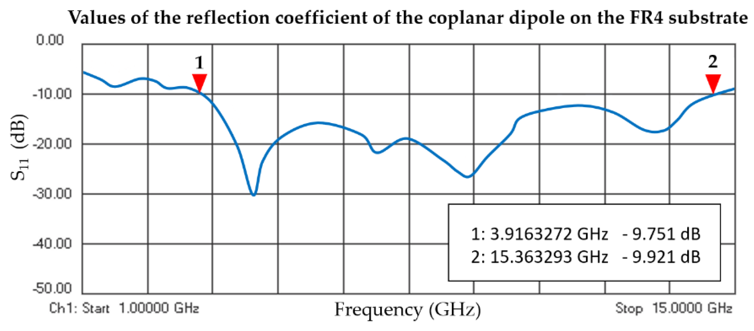
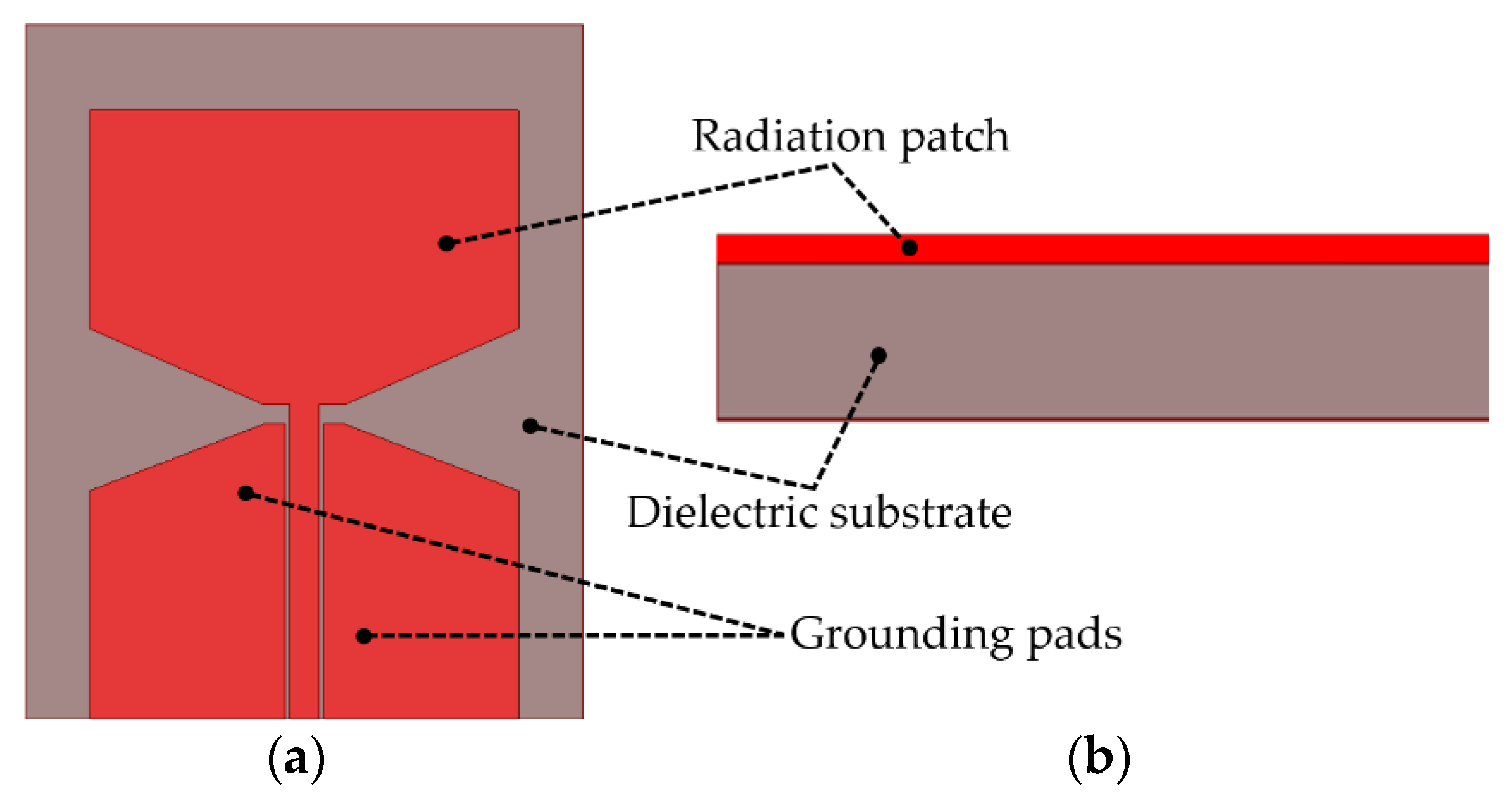
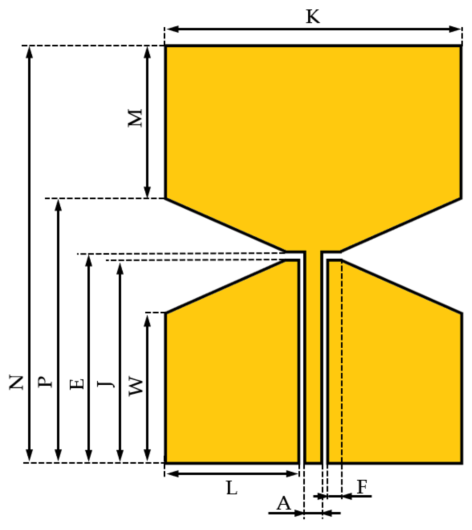
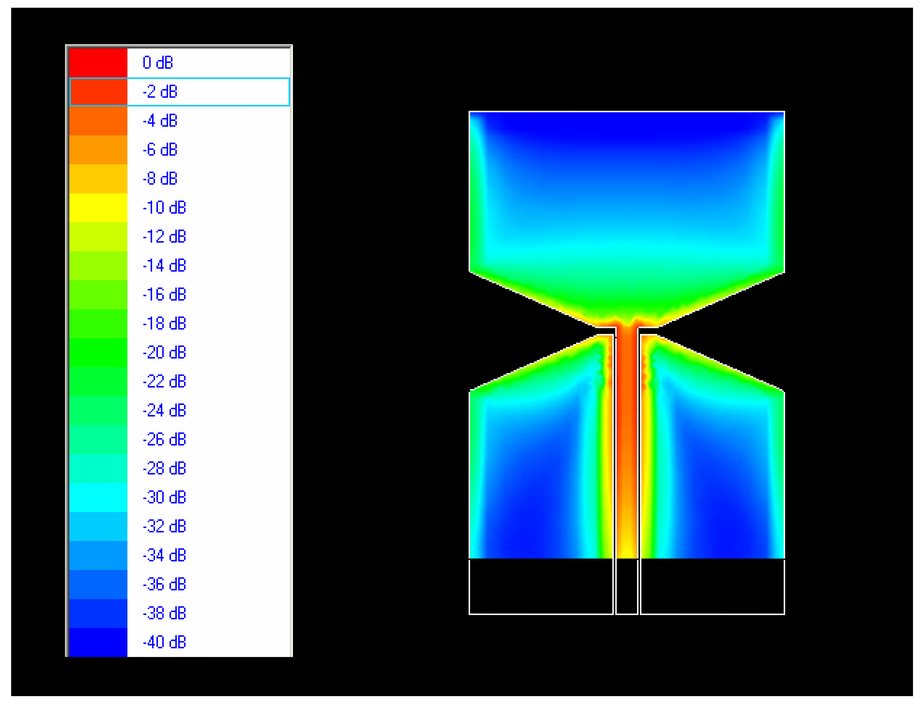
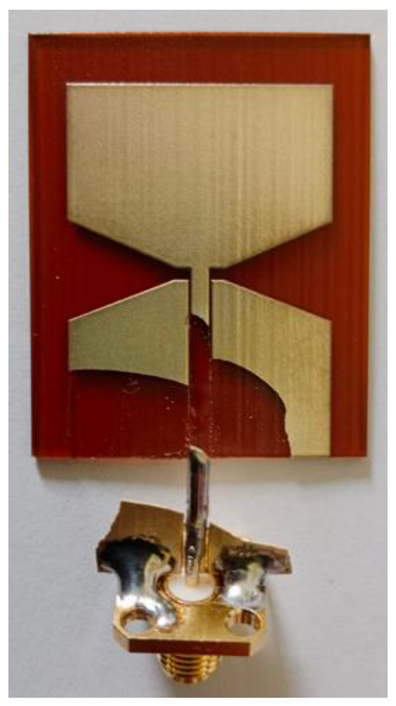
2.3. Design and Analysis of Coplanar Dipole

The coplanar dipole (see Figure 3) has very good broadband properties and is very small, which can be used for the miniaturization of UWB communication systems [13,14,15,16]. Extreme bandwidth systems are among the promising systems for modern radio communication. UWB technology is characterized by a large bandwidth of at least 500 MHz or 20% bandwidth satisfying the condition [17]
B f f c > 0.2
where Bf is the bandwidth for a 10 dB drop, and fc is the center frequency of the band.
In UWB technologies, the bandwidth is used to compare antennas with each other. To make it clear exactly where the Bf value is read, this value is defined for a 3 dB or 10 dB drop. Wideband technologies do not have a harmonic carrier, and the information is encoded in a sequence of very short pulses (0.2 to 1.5 ns) [17]. Each radio channel can have a bandwidth of more than 500 MHz, depending on its center frequency.
A key point in the implementation of UWB systems is the design of the wideband antenna. The advantage of broadband antennas is the slight variation in the electrical parameters over a relatively wide frequency band. The design emphasizes the stability of the input impedance. Our designed patch antenna operates in the band from 3.1 GHz to 10.6 GHz.
Table 2 shows the dimensions of the coplanar dipole for the selected substrates from which the patch antenna was manufactured. The proposed antennas with different types of substrates were simulated, and the results are shown in Figure 4, Figure 5, Figure 6 and Figure 7. The simulation of the coplanar dipole design showed sufficient bandwidth for the reflection coefficient to drop to −10 dB and a better parameter s11. It is clear that the proposed antenna is suitable for broadband applications [18].
Figure 5 shows that FR4 material has parameters that are not ideal for antenna applications. Arlon 25N and 3D material have almost identical properties. Figure 6 shows selected simulations for the antenna on the 3D substrate.

3. Coplanar Dipole Production Technology

Three different technological processes were used to produce the patch antennas. An etching technology was used for the production of the patch antenna on the Arlon 25N substrate (Figure 8b). The antenna on the FR4 substrate was produced by CNC technology (Figure 8a). The 3D-printed antenna is shown in Figure 8c. The production of antennas by etching or CNC technology is sufficiently described in the available literature [18]. We only further analyzed the 3D printing using LDM (lights-out digital additive manufacturing) technology.

3.1. Description of 3D LDM Printing Technology

LDM technology (lights-out digital additive manufacturing) uses simultaneous printing of conductive ink (CI) and dielectric ink (DI). By printing with both inks simultaneously while maintaining a high resolution and maximum accuracy, the DragonFly™ platform has virtually unlimited design flexibility in multiple applications across various industries. These include communications, RF, medical devices, drones, aerospace, automotive, satellites, in-circuit transformers, antennas, coils, capacitors, etc. [19].
The 3D printer has two print heads, one for printing AgCite™ conductive ink (silver nanoparticles suspended in a solvent) and the other for printing dielectric polymer ink. Both inks have unique and compatible sintering and curing properties. The inks are optimized for use in nanotechnologies [19].
When printing, the thickness of one printed layer of conductive ink (CI) varies between 1.9 and 3.2 μm, and for dielectric ink (DI), 0.27 and 0.44 μm. Thus, for one layer of CI, the machine prints about 11 layers of DI (this further depends on the density of the motif and other parameters). However, everything is performed automatically, and DragonFly LDM2 performs an automatic thickness calibration. The time to print one patch antenna using the 3D LDM2 printer is about 5 h. The cost of 3D printing one antenna consists of two items: the price of dielectric ink (DI) is approximately 4.5 EUR, and the price of conductive ink (CI) is 18.5 EUR. It depends on the designed motif and the size of the antenna.
Therefore, the total cost of the antenna is related to the antenna size. However, if we were to produce, for example, a special antenna consisting of dozens of miniature radiation panels, the production cost would still be the same. Complex antennas that are difficult to produce due to their complex shape are produced using other technologies that are already very costly (for example, the antenna array described in the reference [20]). 3D LDM technology allows for the production of antennas with a precision of 1.9–3.2 μm for conductive material and 0.27–0.44 μm when printing dielectric material [21]. This makes this technology quite exceptional.

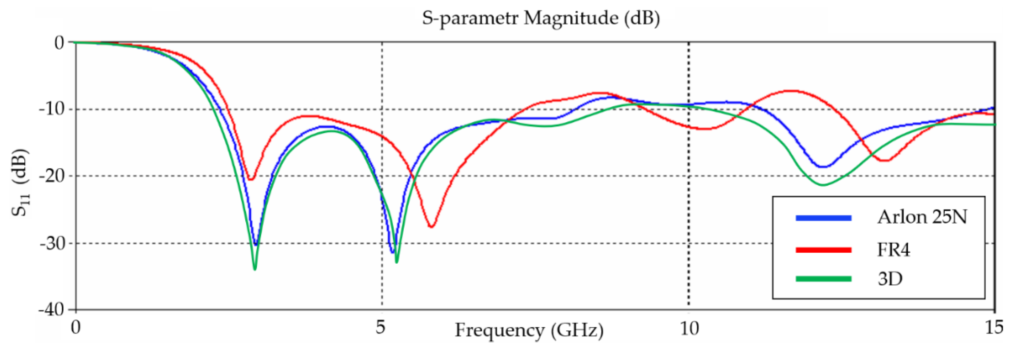
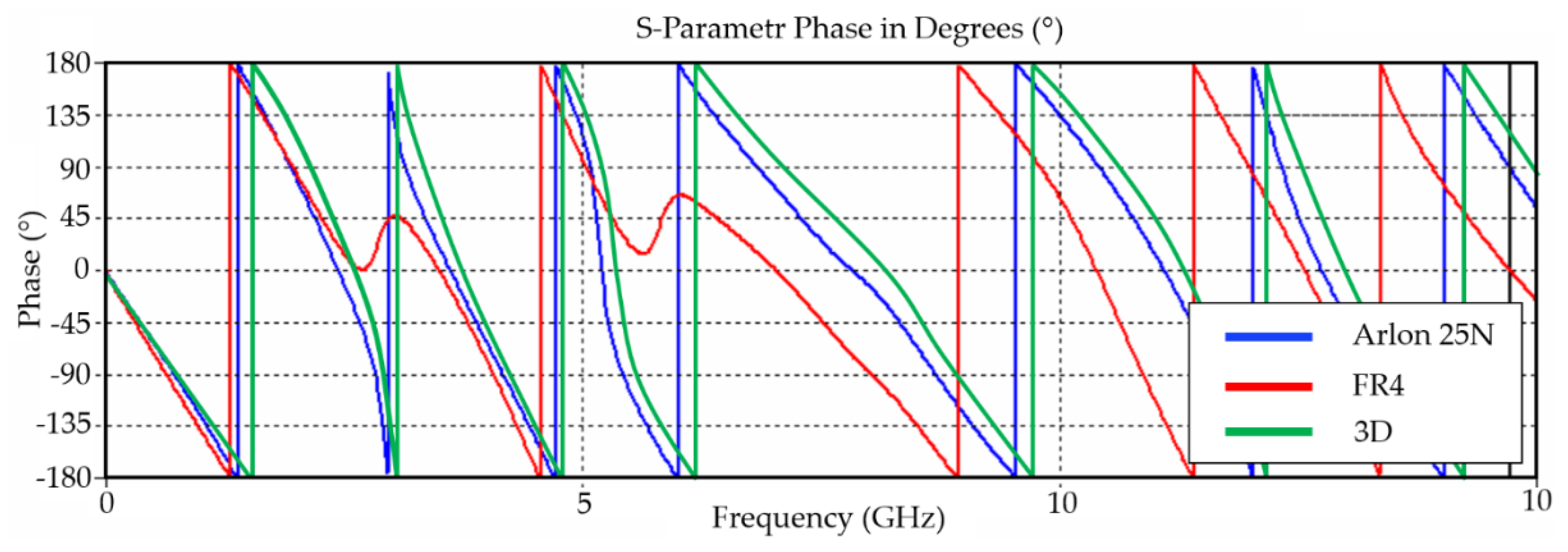
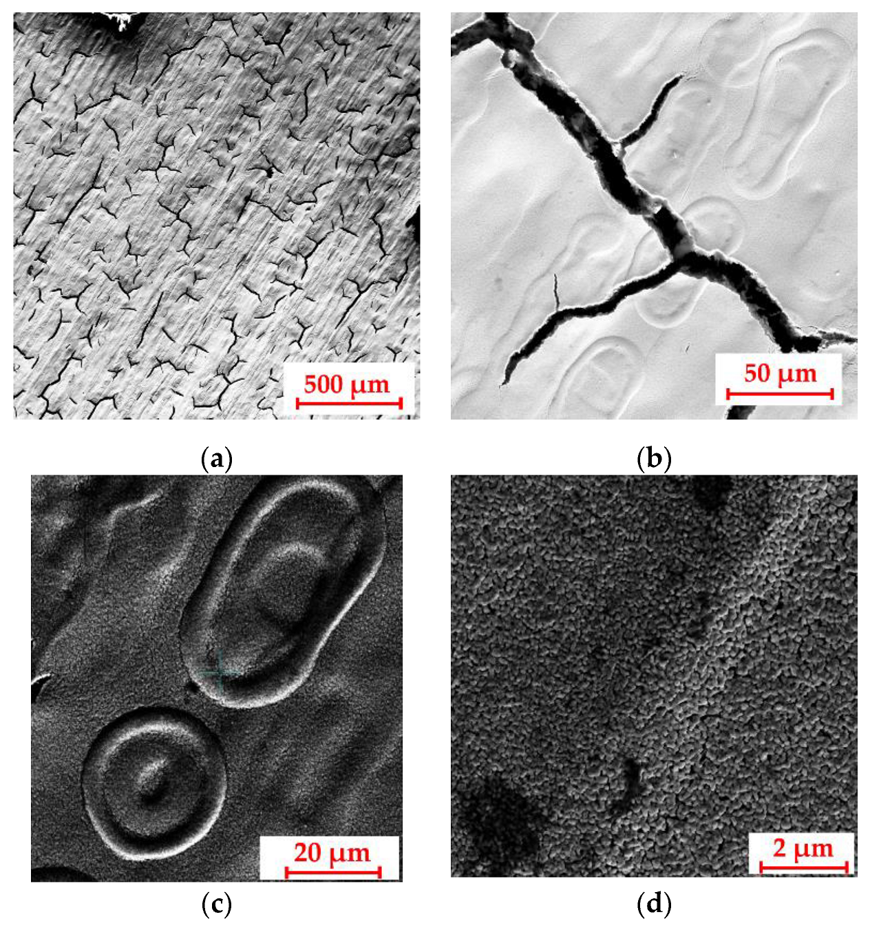
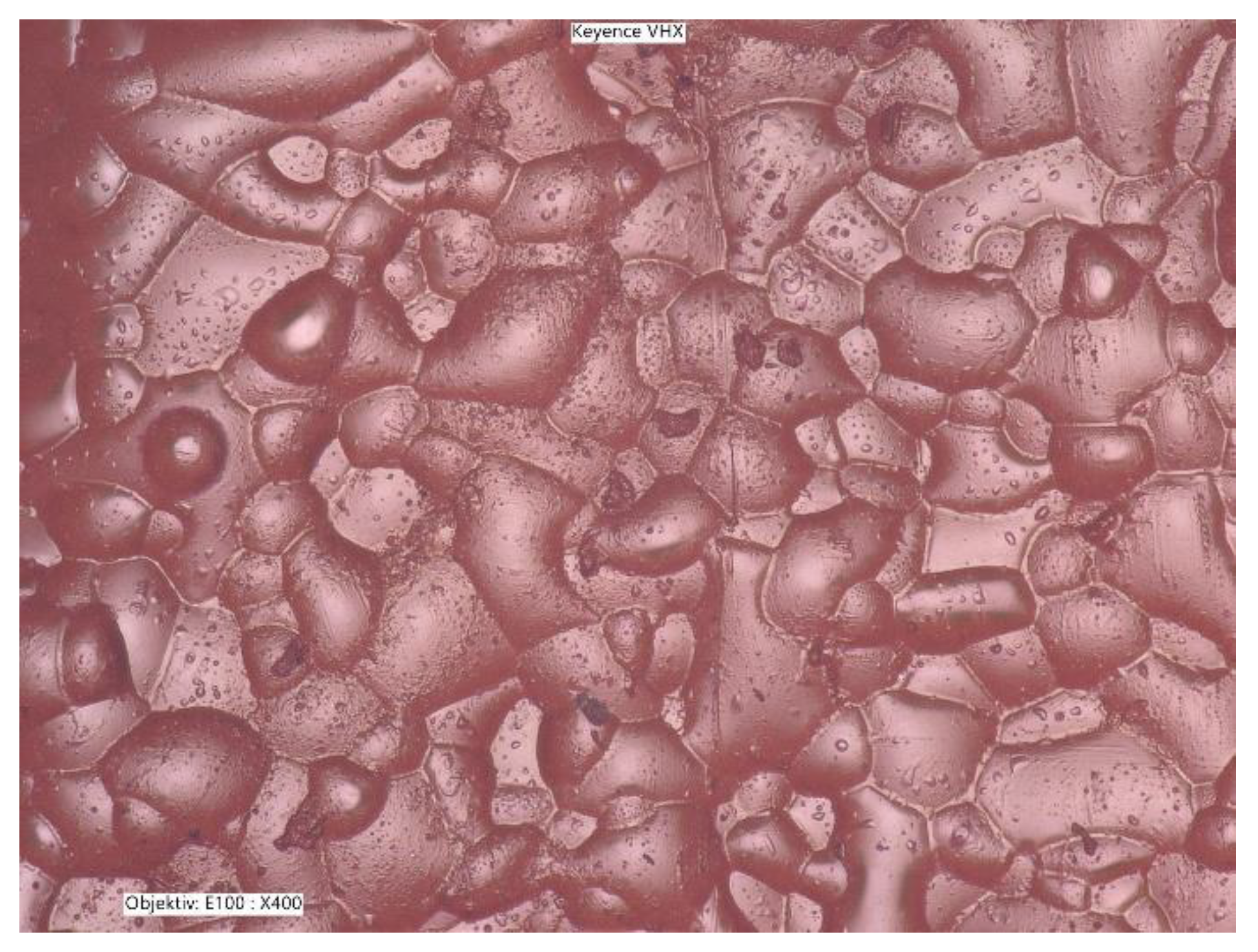
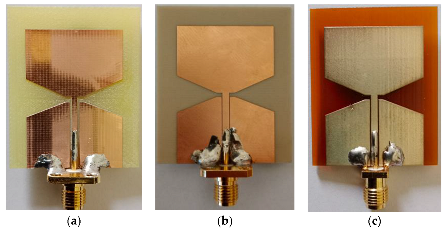
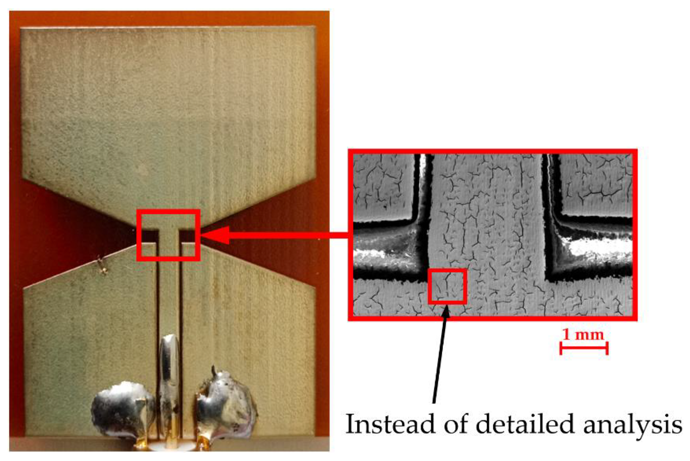
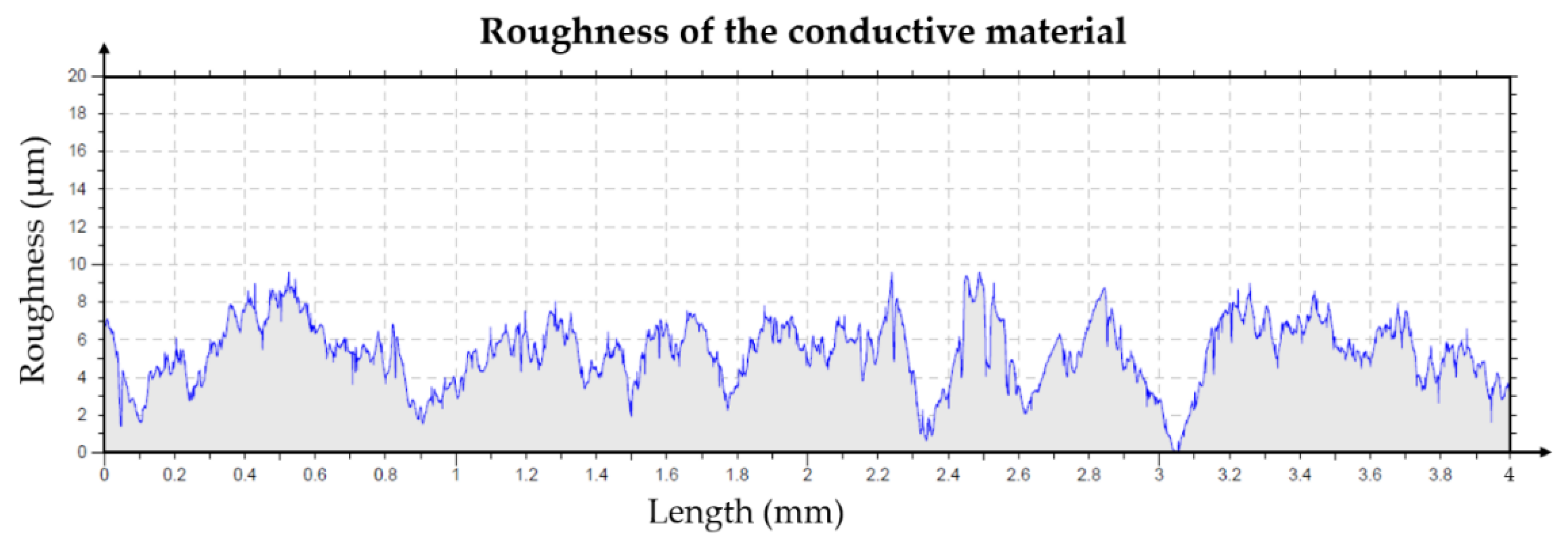
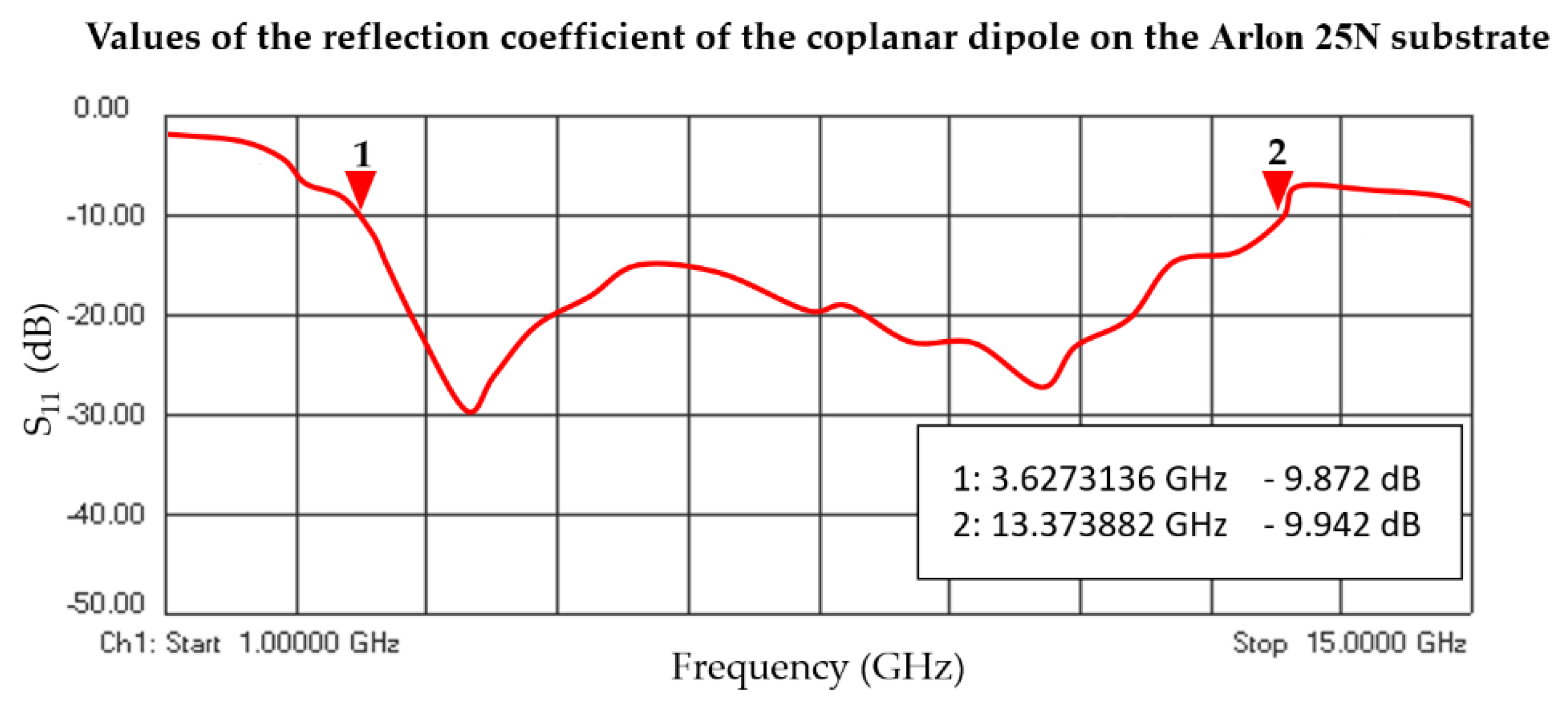
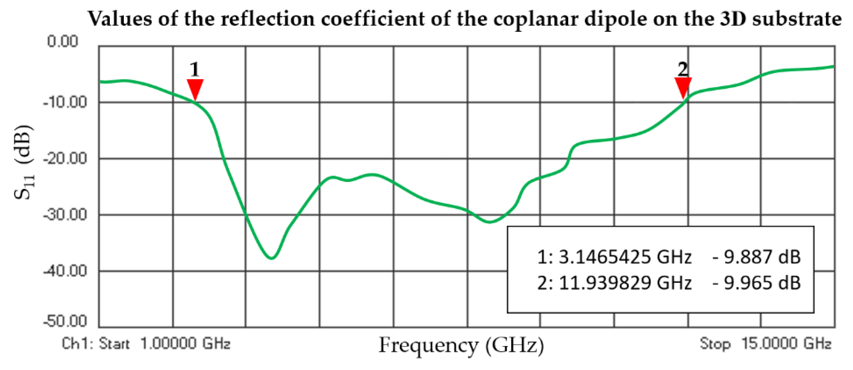
3.2. Technical Analysis of a 3D LDM-Printed Patch Antenna

The surface topography was measured with a Talysurf CLI profilometer using the touch method and evaluated with the TalyMap Platinum software (version 6.2). Pictures of the surface were taken on a Tescan Mira 4 electron microscope. Figure 9 shows an analysis of the 3D LDM-printed surface. Figure 10 shows the surface morphology at different magnifications. Figure 10a shows small cracks reaching 100 µm in length. Figure 10b shows a detail of the crack; we were not able to measure the depth of the crack, but we predicted that it did not extend through the entire thickness of the coating. Figure 10c shows in detail the shape of the traces left by the nozzle after printing. Figure 10d shows the microstructure of the surface, showing that the surface is not homogeneous, as some local imperfections occur. From the results presented below, it is evident that these imperfections on the surface did not affect the function of the antenna. Figure 11 shows a detail of the printed dielectric substrate.
Another test was to determine the roughness and roughness slope of the printed metal layer. A touch sensor was used for the test. The test was carried out according to the ISO 25 178-1 standard at a length of 4 mm and cut-off of 0.8 mm, and a Gaussian filter was used for evaluation [22]. Figure 12 shows the roughness profile of the conductive material. The main test parameters are the following:
-
Roughness average Ra = 1.15 μm;
-
Mean roughness depth Rz = 6.78 μm;
-
Total height of the roughness profile Rt = 7.86 μm;
-
Arithmetic mean slope Rda = 7.62°;
-
Root mean square slope of the assessed profile Rdq = 14.6°.
Thanks to a detailed technical analysis of the 3D-printed patch antenna, it was found that 3D LDM printing technology has very high-quality parameters and is suitable for the production of the proposed patch antenna.
During handling of the 3D-printed antenna, it was discovered that this antenna is very fragile. Figure 13 shows the damaged antenna after a 1 m fall to the ground. This fragile feature could be eliminated, for example, by placing the antenna into a protective housing. Future research will explore the options for strengthening this type of antenna. However, the main purpose of this 3D method is to manufacture prototypes of geometrically complex antennas, where high demands are placed on precision manufacturing. One major advantage of this 3D method is that the cost of production does not increase with the complexity of the antenna structure.
Further research can focus on a better adaptation of the design rules using LDM technology to fully exploit the options of 3D space and to explore other options of antenna design [18], to improve the solder pad arrangement and the connectors, and to make the soldering method more suitable to this technology.

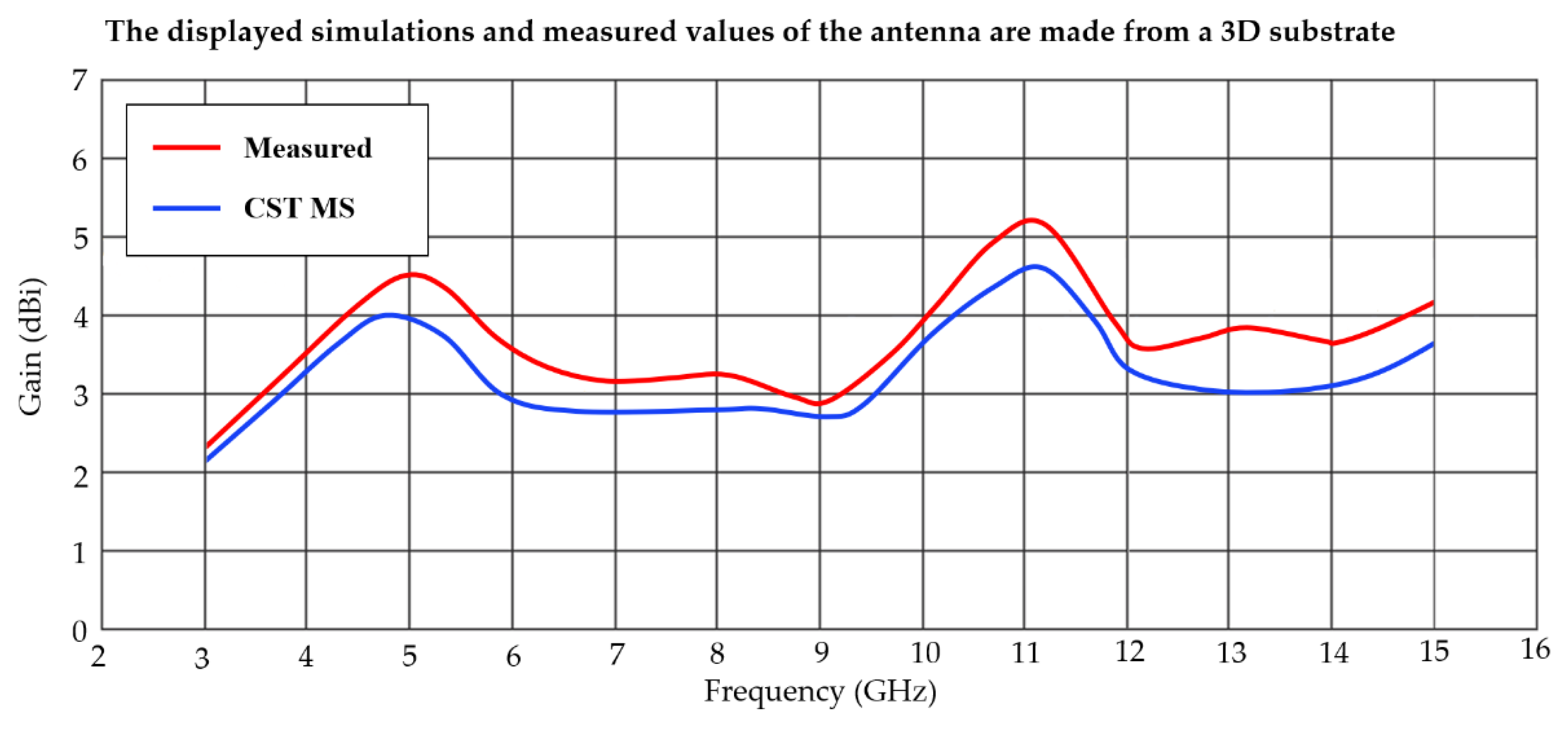
4. Evaluation of 3D LDM Printing Technology

All three manufactured antennas were analyzed using a vector analyzer. The results showed that the printed patch antenna has very good performance compared with conventional production techniques (Figure 14, Figure 15 and Figure 16). The bandwidth of the reflection coefficient for a 10 dB drop is from 3.34 GHz to 11.06 GHz. It thus suits planar antennas for UWB applications.

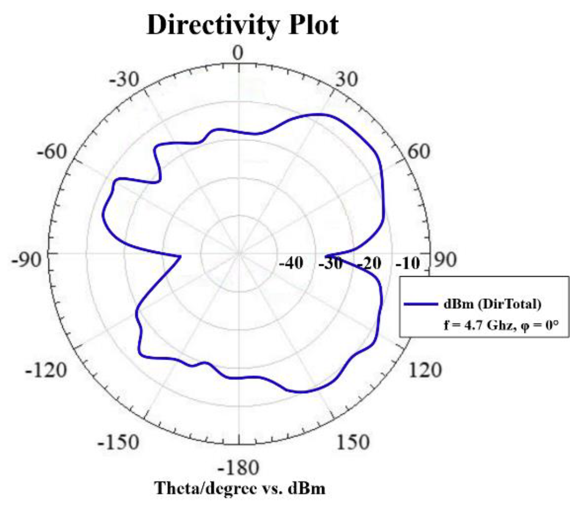
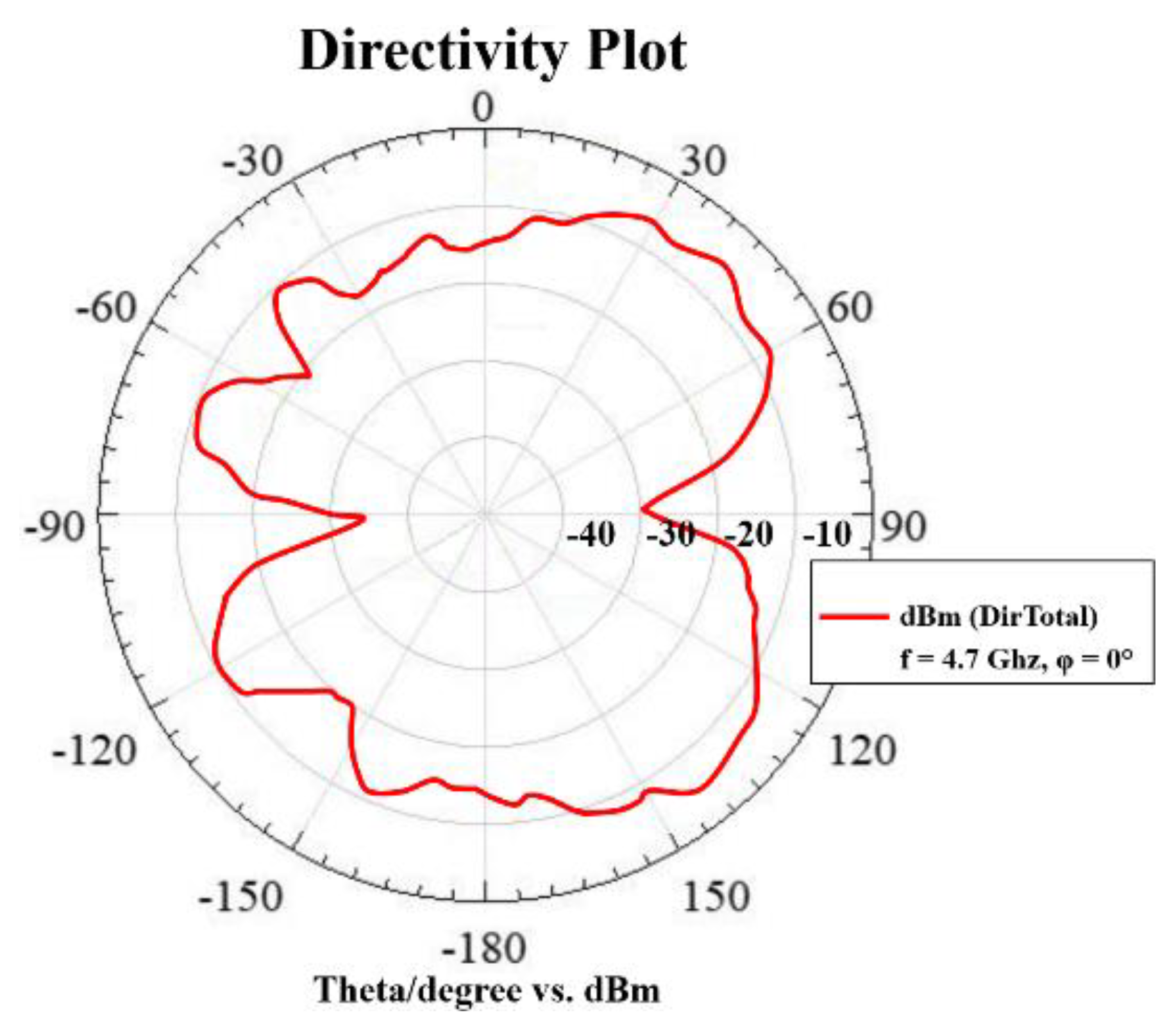
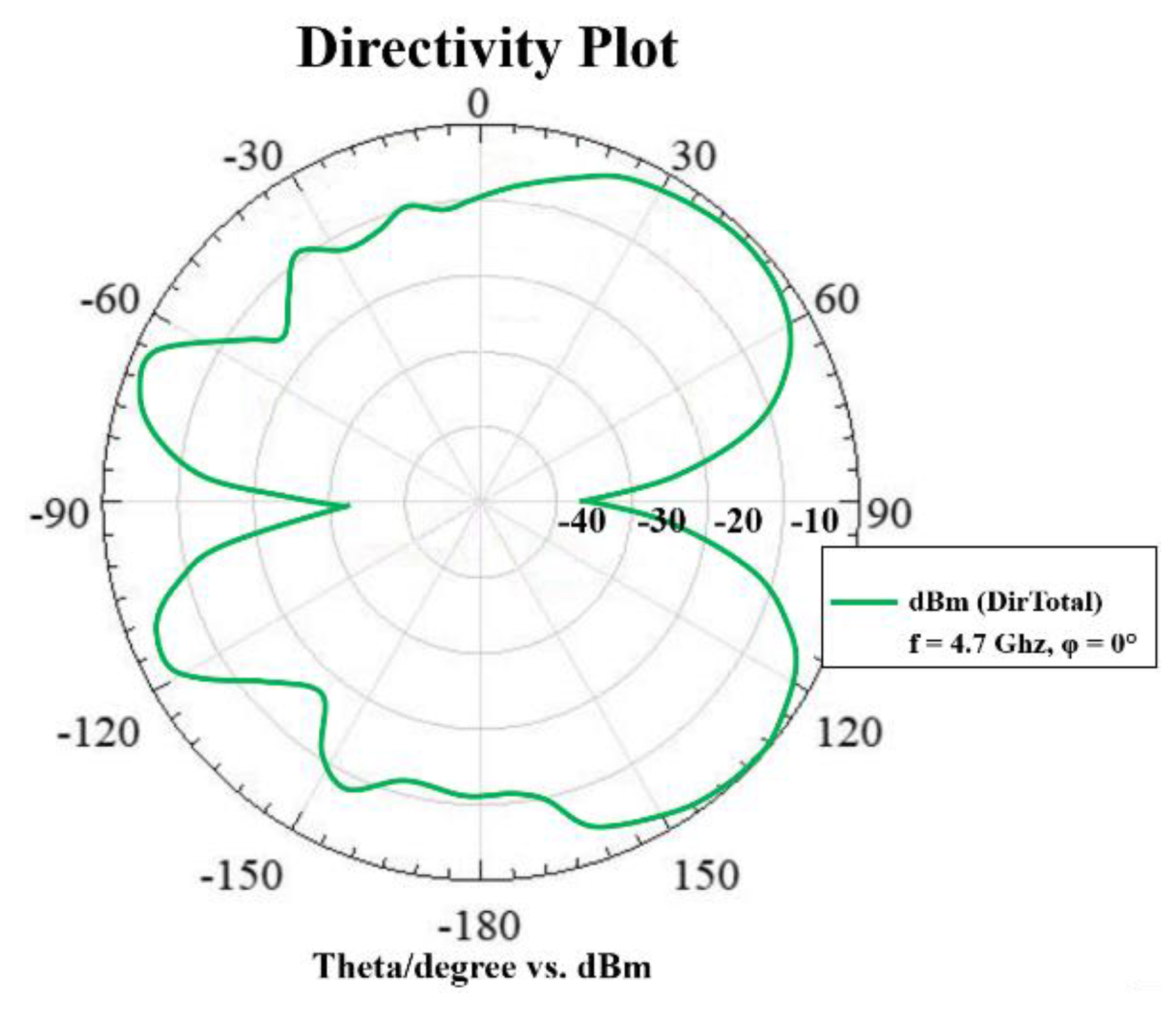
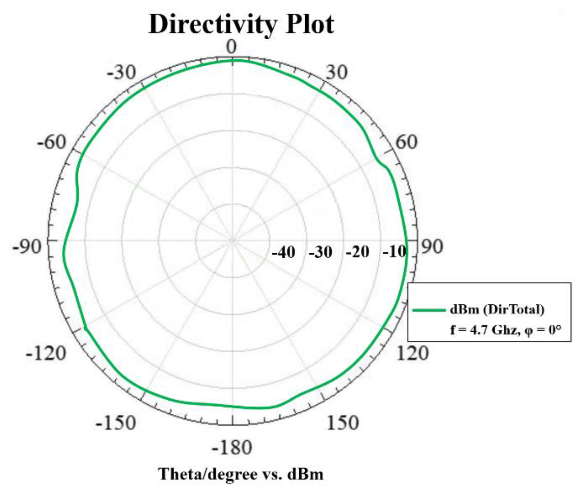
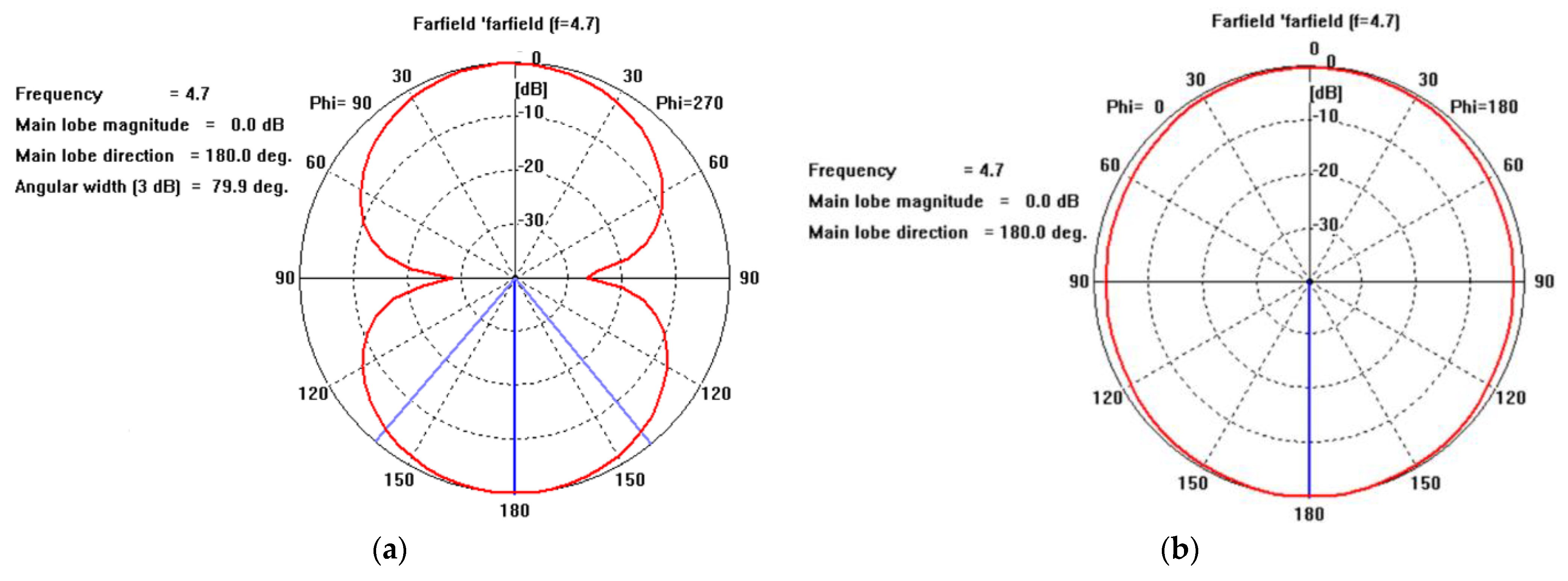
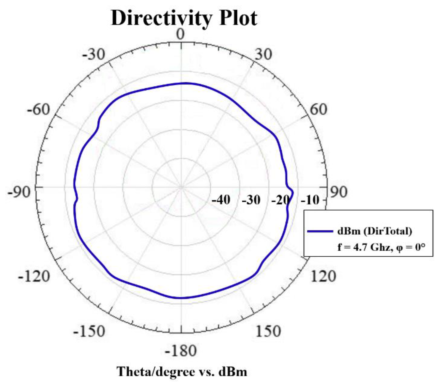
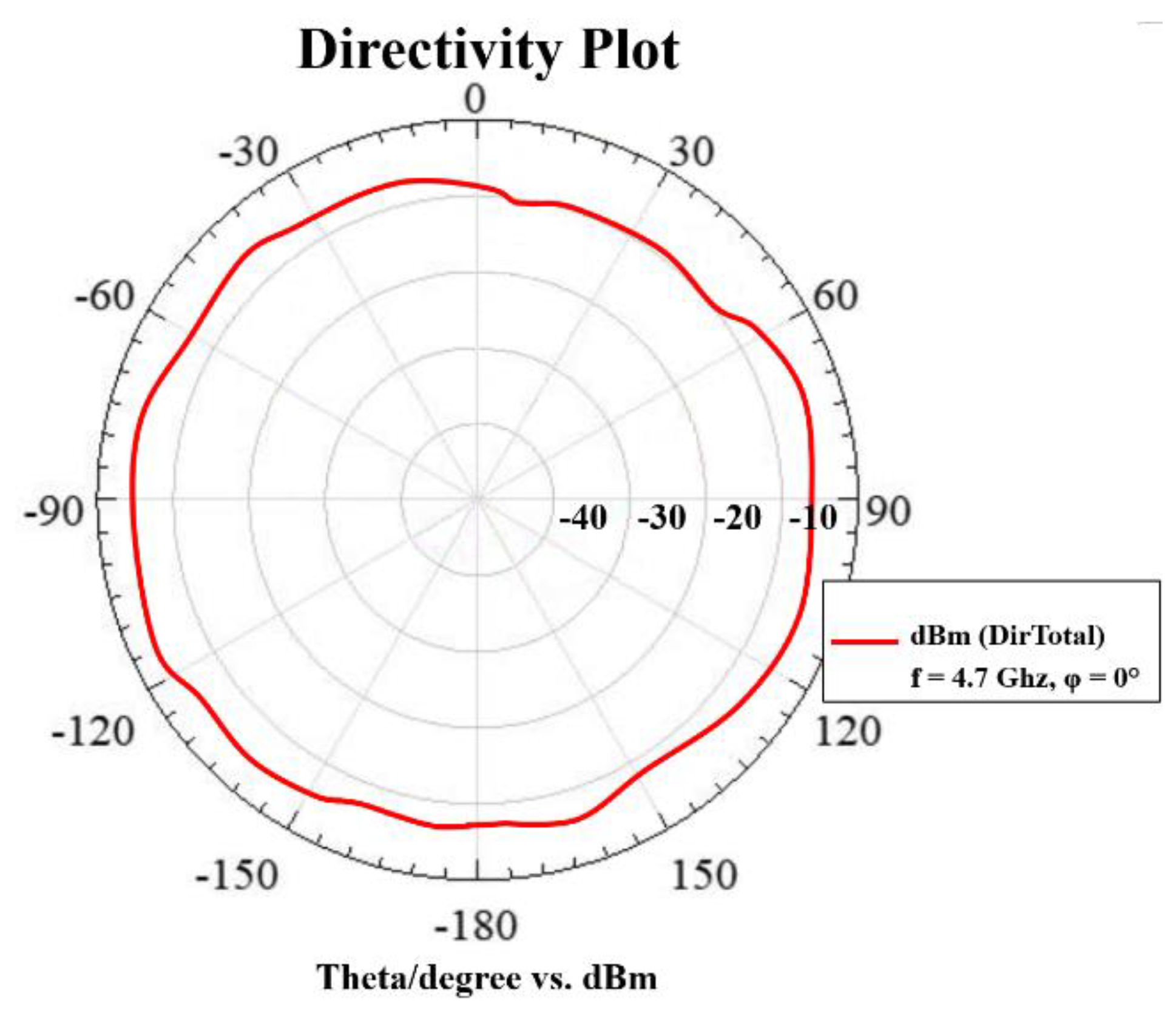
Radiation Patterns of Far-Field Patch Antennas in the E- and H-Planes

Further tests were carried out in an anechoic chamber. The description of the test is described in detail in [17]. Figure 17, Figure 18 and Figure 19 show the measured far-field directional characteristics in the E-plane at 4.7 GHz for the produced coplanar dipole antenna.
Figure 20, Figure 21 and Figure 22 show the measured far-field directional characteristics in the H-plane at 4.7 GHz for the produced coplanar dipole antenna.
Figure 23 shows the measured and simulated gain of a coplanar dipole on a 3D substrate. In our case, the measurement was better than the simulation itself. This could be due to the type and density of the mesh network and also the type of computational solver.

5. Conclusions

In this paper, the production of a coplanar dipole using a new 3D LDM printing technology was presented. Usually, this technology is used for PCB manufacturing. However, here, it was used as an alternative method to manufacture a 3D-printed antenna in order to study the RF properties of the conductive and dielectric ink of the LDM technology. The selected antenna was also designed and manufactured on two conventional dielectric substrates using standard manufacturing procedures. These two conventional coplanar dipole antennas were compared with the antenna manufactured with the new 3D LDM technology.
Measurements showed that the 3D LDM-printed patch antenna has a radiation pattern that matches theoretical predictions. The main advantage of the LDM technology is the high quality of the print. LDM technology can print with low roughness—top surface <2 μm, bottom surface <0.25 μm, and with a minimum particle size of 80 nanometers (d50). Such parameters allow for the printing of 3D miniature objects with high precision. LDM technology is also suitable for the production of coplanar dipole antennas due to the properties of the dielectric materials used for 3D printing. A 3D-printed antenna has a similar weight compared with antennas on conventional substrates.
One disadvantage of the 3D LDM printing technology is that the printed objects are very fragile. Shaping or bending of these 3D-printed objects is very limited (however, this depends on the thickness of the PCB). 3D LDM-printed objects must be handled with great care. Based on the performed tests, it can be said that the 3D LDM technology is applicable for printing planar antennas. In the future, it is possible to fully exploit a new specific approach and implement completely new design rules. This approach would move away from the compared conventional technologies (i.e., etching or milling) toward a spatial arrangement of structural elements in thicknesses of up to 3 mm.

Author Contributions

Conceptualization, M.P. and J.O.; methodology, M.P.; validation, M.P., Z.J. and M.K.; formal analysis, J.O. and M.P.; resources, M.P., Z.P., L.P. and P.J.; data curation, M.P.; writing—original draft preparation, M.P.; writing—review and editing, J.O., Z.P., L.P., P.J., Z.J. and M.K. visualization, M.P.; project administration, J.O.; funding acquisition, J.O. All authors have read and agreed to the published version of the manuscript.

Funding

The presented research was supported by the Czech Ministry of Defence (AIROPS and VAROPS, the University of Defence Development Program), the Technology Agency of the Czech Republic (TM02000035, NEOCLASSIG), the Internal Grant Agency of Brno University of Technology (project no. FEKT-S-23-8191), and Nanodimension Academia Partnership.

Institutional Review Board Statement

Not applicable.

Informed Consent Statement

Not applicable.

Data Availability Statement

The data presented in this study are available on request from the corresponding author.

Conflicts of Interest

The authors declare no conflict of interest, and the funders had no role in the design of the study; in the collection, analyses, or interpretation of the data; in the writing of the manuscript; or in the decision to publish the results.

References

  1. Richterová, M.; Popela, M.; Olivová, J.; Fritz, D. Antennas Based on Metamaterials and Their Application in Modern Communication Technologies; Mechanisms and Machine Science; Springer Science and Business Media: Berlin/Heidelberg, Germany, 2023; ISBN 978-3-031-15757-8. ISSN 2211-0984. [Google Scholar] [CrossRef]
  2. Popela, M.; Vaněk, S.; Olivová, J.; Vavrečková, K. 3D printing of a patch antenna for 5G network and radio monitoring of UWB signals. In Proceedings of the 9th International Conference on Military Technologies (ICMT), Brno, Czech Republic, 23–26 May 2023; ISBN 979–8-3503-2569-0. [Google Scholar] [CrossRef]
  3. Olivová, J.; Popela, M.; Richterová, M.; Štefl, E. Use of 3D Printing for Horn Antenna Manufacturing. Electronics 2022, 11, 1539. [Google Scholar] [CrossRef]
  4. Richterová, M.; Olivová, J.; Popela, M.; Blazek, V. Minkowski Fractal Antenna Based on 3D Printing. In IOP Conference Series: Materials Science and Engineering; Miclaus, S., Ed.; IOP Publishing Ltd.: Sibiu, Romania, 2022; ISSN 1757-8981. [Google Scholar] [CrossRef]
  5. Hoyack, M.; Bjorgaard, J.; Huber, E.; Mirzaee, M.; Noghanian, S. Connector design for 3D printed antennas. In Proceedings of the 2016 IEEE International Symposium on Antennas and Propagation (APSURSI), Fajardo, PR, USA, 26 June–1 July 2016. [Google Scholar] [CrossRef]
  6. Toy, Y.C.; Mahouti, P.; Güneş, F.; Belen, M.A. Design and manufactering of an X-band horn antenna using 3D printing technology. In Proceedings of the 8th International Conference on Recent Advances in Space Technologies (RAST), Istanbul, Turkey, 19–22 June 2017. [Google Scholar] [CrossRef]
  7. Jiménez, J.; Irigoyen, J.; Aresti, M.; Ederra, I.; Bravo, J.; Iriarte, J.C. A New ABS Conductive Material to develop Fully 3D-Printed Patch Antennas. In Proceedings of the 17th European Conference on Antennas and Propagation (EuCAP), Florence, Italy, 26–31 March 2023. [Google Scholar] [CrossRef]
  8. Balanis, C.A. Antenna Theory: Analysis and Design; John Wiley & Sons: Hoboken, NJ, USA, 2016; ISBN 978-1118642061. [Google Scholar]
  9. Jeongpyo, K.; Taeyeoul, Y.; Jaemoung, K.; Jaehoon, C. Design of an Ultra Wide-band Printed Monopole Antenna Using FDTD and Genetic Algorithm. IEEE Microw. Wirel. Compon. Lett. 2005, 15, 395–397. [Google Scholar] [CrossRef]
  10. Noor, S.K.; Jusoh, M.; Sabapathy, T.; Rambe, A.H.; Vettikalladi, H.; Albishi, M.A.; Himdi, M. A Patch Antenna with Enhanced Gain and Bandwidth for Sub-6 GHz and Sub-7 GHz 5G Wireless Applications. Electronics 2023, 12, 2555. [Google Scholar] [CrossRef]
  11. Raida, Z.; Černohorský, D.; Gala, D.; Goňa, S.; Nováček, Z.; Otevřel, V.; Michálek, V.; Navrátil, V.; Urbanec, T.; Škvor, Z.; et al. Multimedia Textbook. Brno: FEEC VUT Brno. Available online: https://www.radio.feec.vutbr.cz/raida/multimedia/index.php?lang=en (accessed on 1 January 2020).
  12. Industrial 3DPrinting of Electronics for Manufacturing, A.M.E. NanoDimension. Available online: https://www.nano-di.com (accessed on 19 October 2023).
  13. Martínez-Lozano, A.; Blanco-Angulo, C.; García-Martínez, H.; Gutiérrez-Mazón, R.; Torregrosa-Penalva, G.; Ávila-Navarro, E.; Sabater-Navarro, J.M. UWB-Printed Rectangular-Based Monopole Antenna for Biological Tissue Analysis. Electronics 2021, 10, 304. [Google Scholar] [CrossRef]
  14. Jayant, S.; Srivastava, G.; Kumar, S.; Mostafa, H.; Goyal, B.; Choi, H.C.; Kim, K.W. Decoupling Methods in Planar Ultra-Wideband Multiple-Input-Multiple-Output Antennas: A Review of the Design, State-of-the-Art, and Research Challenges. Electronics 2023, 12, 3813. [Google Scholar] [CrossRef]
  15. Savcı, H.Ş. A Four Element Stringray-Shaped MIMO Antenna System for UWB Applications. Micromachines 2023, 14, 1944. [Google Scholar] [CrossRef] [PubMed]
  16. Kiani, S.H.; Savci, H.S.; Munir, M.E.; Sedik, A.; Mostafa, H. An Ultra-Wide Band MIMO Antenna System with Enhanced Isolation for Microwave Imaging Applications. Micromachines 2023, 14, 1732. [Google Scholar] [CrossRef] [PubMed]
  17. Garg, R.; Bhartia, P.; Bahl, I.; Ittipiboon, A. Microstrip Antenna Design Handbook; Artech House, Inc.: Boston, MA, USA; London, UK, 2001; ISBN 0-89006-513-6. [Google Scholar]
  18. Vavrečková, K.; Olivová, J.; Richterová, M.; Popela, M. Patch Antenna for Monitoring UWB Signals. In Proceedings of the International Conference on Military Technologies (ICMT), Brno, Czech Republic, 8–11 June 2021. [Google Scholar] [CrossRef]
  19. McMahan, S. 3D Printing Enables ‘Lights-Out Digital Manufacturing’ of Electronic Circuitry. Available online: https://eepower.com/news/3d-printing-of-electronics-with-little-to-no-human-intervention/# (accessed on 23 October 2023).
  20. Rahyanditya, I.; Rahyanditya, I.; Adit, K. Design and implementation of microstrip antenna array on Ku-Band for satellite TV reception. In Proceedings of the International Telecommunication Networks and Applications Conference (ITNAC), Sydney, NSW, Australia, 18–20 November 2015. [Google Scholar] [CrossRef]
  21. Storz, V. Nanodimension. Available online: https://www.linkedin.com/pulse/sphere-phased-array-antenna-valentin-storz/ (accessed on 19 October 2023).
  22. ČSN EN ISO 178 (640607); Plasty—Stanovení Ohybových Vlastností. Český Normalizační Institut: Prague, Czech Republic, 2003. Available online: https://www.technicke-normy-csn.cz/csn-en-iso-178-640607-211909.html (accessed on 19 October 2023).
Figure 1. Description of a patch coplanar dipole: (a) view from above; (b) side view.
Applsci 14 01556 g001
Figure 2. Display of a connector attached to an antenna made with LDM technology.
Applsci 14 01556 g002
Figure 3. Dimensions of coplanar dipole.
Applsci 14 01556 g003
Figure 4. Modulus of reflection coefficient of coplanar dipole with different substrate types (modeled in CST).
Applsci 14 01556 g004
Figure 5. Phase of reflection coefficient of coplanar monopole with different substrate types (modeled in CST).
Applsci 14 01556 g005
Figure 6. Radiation patterns of far-field in the E-plane (a) and H-plane (b) at 4.7 GHz for a coplanar dipole on 3D substrate and simulated in CST.
Applsci 14 01556 g006
Figure 7. Current distribution on coplanar dipole—frequency 3.1 GHz.
Applsci 14 01556 g007
Figure 8. Image of coplanar dipole fabricated on (a) FR4 material; (b) Arlon 25N; (c) 3D substrate.
Applsci 14 01556 g008
Figure 9. Imaging the location of a detailed analysis of a coplanar dipole using a 3D substrate.
Applsci 14 01556 g009
Figure 10. Coplanar dipole imaging with the Olympus MVX10 microscope; (a) are small cracks, (b) is a detail of the crack, (c) is in detail the shape of the traces left by the nozzle after printing, (d) is the micro-structure of the surface.
Applsci 14 01556 g010
Figure 11. Dielectric imaging with the Olympus MVX10 microscope (400× magnified).
Applsci 14 01556 g011
Figure 12. Display of the roughness of the conductive material.
Applsci 14 01556 g012
Figure 13. Representation of the destruction of a 3D-printed coplanar dipole.
Applsci 14 01556 g013
Figure 14. Detail of the measured reflection coefficient of coplanar dipole on FR4 substrate ranging from 1 to 15 GHz.
Applsci 14 01556 g014
Figure 15. Detail of the measured reflection coefficient of coplanar dipole on Arlon 25N substrate ranging from 1 to 15 GHz.
Applsci 14 01556 g015
Figure 16. Detail of the measured reflection coefficient of coplanar dipole on 3D-printed substrate ranging from 1 to 15 GHz.
Applsci 14 01556 g016
Figure 17. Radiation patterns of far-field in the E-plane at 4.7 GHz for the produced coplanar dipole on an FR4 substrate.
Applsci 14 01556 g017
Figure 18. Radiation patterns of far-field in the E-plane at 4.7 GHz for the produced coplanar dipole on an Arlon 25N substrate.
Applsci 14 01556 g018
Figure 19. Radiation patterns of far-field in the E-plane at 4.7 GHz for the produced coplanar dipole on 3D printed substrate.
Applsci 14 01556 g019
Figure 20. Radiation patterns of far-field in the H-plane at 4.7 GHz for a coplanar dipole produced on an FR4 substrate.
Applsci 14 01556 g020
Figure 21. Radiation patterns of far-field in the H-plane at 4.7 GHz for the produced coplanar dipole on an Arlon 25N substrate.
Applsci 14 01556 g021
Figure 22. Radiation patterns of far-field in the H-plane at 4.7 GHz for the produced coplanar dipole on 3D printed substrate.
Applsci 14 01556 g022
Figure 23. Measured and simulated antenna gain.
Applsci 14 01556 g023
Table 1. Relative permittivity εr and loss factor tg(δ) for the 3D material [12]. Note: dielectric breakdown voltage thickness 0.6 mm for 40.3 KV [12].
200 MHz500 MHz1 GHz2 GHz5 GHz10 GHz15 GHz20 GHz
εr2.802.812.812.802.802.782.752.78
tg(δ) 0.0010.0040.0060.0110.0120.0130.0130.012
Table 2. Dimensions of coplanar dipole, parameters of used substrates.
SubstrateDimensions of a Coplanar Dipole
εr
(-)
h
(mm)
W
(mm)
L
(mm)
A
(mm)
J
(mm)
N
(mm)
M
(mm)
P
(mm)
E
(mm)
G
(mm)
K
(mm)
FR44.401.5011.7410.031.5015.6531.3011.2420.0616.150.2222.00
25N3.281.5013.1411.231.6816.9835.0612.5922.4718.090.2524.64
3D2.731.5016.1212.541.7818.6339.0215.0124.1220.560.3027.12
Disclaimer/Publisher’s Note: The statements, opinions and data contained in all publications are solely those of the individual author(s) and contributor(s) and not of MDPI and/or the editor(s). MDPI and/or the editor(s) disclaim responsibility for any injury to people or property resulting from any ideas, methods, instructions or products referred to in the content.

