1. Introduction
Lately, there has been significant interest in microwave and millimeter-wave communication systems that function in the Ka- to F-band. These systems are valued for their broad operational bandwidth, fast data transfer, affordable production, and excellent performance. CMOS integrated circuits are seen as potential choices due to their circuit implementations, which offer advantages such as low supply voltage, low cost, and high integration [
1].
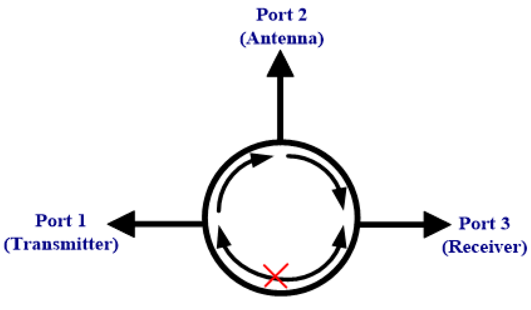
Active circulators are functional components with three ports that are specifically designed for integrated system-on-chip (SoC) applications. These components are appropriate for use with monolithic microwave integrated circuit (MMIC) integration. The relevant literature references for further information on this topic are [
2,
3,
4]. These circulators play a crucial role in MMIC integration by allowing signals to flow in a single direction, ensuring optimal impedance at all three ports. Therefore, the transmitter and receiver have the capability to both translate and receive RF signals concurrently, even if they have different frequencies, without the need for a diplexer filter or RF switch. Furthermore, active circulators possess a wide frequency range, minimal signal loss, and compact chip size. Nevertheless, active circulators give rise to issues in transmitting signals from port 3 to port 1. To address the issue of receiver signal leakage into the transmitter port, one can employ quasi-circulators that facilitate just two power flows in the same direction, specifically from port 1 to port 2 and from port 2 to port 3. Various configurations of active quasi-circulator modules have been introduced in microwave and millimeter-wave system applications. One such design involves separating the broadcast and received signals.
Historically, the bulk of circulators have utilized ferrite components. These devices rely on the collective physical characteristics of magnetic materials [
5]. These devices have a limited bandwidth and are too big to be incorporated into monolithic circuits. Precise fabrication of semiconductor devices can be achieved to meet specific criteria rather than relying on the inherent physical properties of the chips. Moreover, these dynamic circulators are more suitable for SoC applications that utilize compact microcontroller integration. In 1965, there was a proposal to develop active circulators that operated at a frequency of three megahertz (MHz) [
6].
A novel active quasi-circulator (QC) module was subsequently designed to enable the incorporation of three ports. This module consisted of transistors equipped with non-reciprocal phase shifters, and its purpose was to attain a level of isolation of 20 dB. Nevertheless, it possesses a substantial chip area and a considerable direct current power consumption [
7]. A novel approach was suggested to minimize the utilization of direct current by employing the phase cancellation technique and leveraging the current-reuse topology [
8]. A 30 GHz quasi-circulator currently employs the current-reuse technique to minimize power consumption [
9]. However, the achieved level of isolation was just 12 dB. The current technology used to decrease chip size and power consumption still has unresolved problems related to narrow band and low isolation [
10]. A quasi-circulator employs a power coupler to enhance isolation, although this coupler restricts its bandwidth. In active quasi-circulators, the utilization of common-source/drain designs has been employed to increase the bandwidth, albeit at the expense of higher insertion loss and noise figure (NF) [
11]. A study has documented the existence of a quasi-circulator with high insertion gain. However, it should be noted that this quasi-circulator has a limited operating bandwidth. The quasi-circulator, which utilizes phase correction, has successfully attained high port-to-port isolation and wideband operation. Nevertheless, the impedance matching network is intricate and requires a significant amount of space on the device. The active balun and current combiner are utilized to attain a condensed form and facilitate straightforward impedance matching [
12]. Nevertheless, these gadgets will diminish the available bandwidth. According to reports, a quasi-circulator that utilizes CMOS technology achieves high gain and excellent isolation. The quasi-circulator’s operational bandwidth remains limited, and its power consumption is significant. However, the problem of limited operational bandwidth has not yet been resolved. The active distributed amplifiers provide a number of advantages, such as ultra-broadband, good gain flatness, and strong insertion gain [
13]. These advantages make them suitable for wideband applications and provide good port-to-port isolation. A self-equalization strategy has been suggested for the active quasi-circulator [
14]. The fundamental configuration comprises a distributed balun connected in series with a distributed combiner, both implemented using GaAs technology. A novel ultra-wideband quasi-circulator using the cascading distributed architecture implemented by 90 nm CMOS achieved high performance of ultra-wideband, good insertion gain, and small chip area, but the port-to-port isolation is not good [
15]. Implementing a quasi-circulator in higher frequency, ultra-wideband, and high isolation using 90 nm CMOS technology is a significant hurdle.
This study presents a novel quasi-circulator design that features a compact architecture primarily composed of three CS FETs. The quasi-circulator functions within the frequency range of C-band to K-band. Furthermore, the phase cancellation approach can be used to achieve higher isolation and broadband performance in |S31| for quasi-circulator applications. The circuit also achieves a good performance of power consumption compared with the state-of-the-art research.
The subsequent sections of this work are structured in the following manner:
Section 2 outlines the design concept, provides a thorough analysis of the detailed design for optimizing circuit parameters, and describes the execution of the suggested quasi-circulator.
Section 3 presents the experimental findings.
Section 4 concludes the text briefly.
2. Circuit Design and Implementation
The suggested design of the ultra-broadband quasi-circulator consists of an active balun that is built using a distributed amplifier with a cascading structure. It also includes a phase inversion channel to promote isolation, as depicted in
Figure 1. The distributed balun can be seen as a series of interconnected distributed amplifiers without a termination at port 2. The incident signal from port 1 travels over the gate terminal of the distributed balun with a sectional phase constant. The voltage, Vgs1, across each gate capacitor of the field-effect transistor causes a current to flow into the drain terminal. By carefully choosing the FET dimension and circuit parameter, the phase velocities of the gate and drain terminals can be regulated to be almost equal. This leads to the sum of the forward direction as they reach port 2. The intrinsic phase inversion characteristic of the common-source field-effect transistor (FET) allows for the attainment of the antiphase output from port 2. In addition, the drain current generated by the cross voltage, Vgs2, flows into the drain terminal of the cascading stage and subsequently to the forward combination at port 3. The double-phase inversion produces a non-inverting phase output at port 3. Therefore, the balun can achieve equal output power and antiphase relationship between ports 2 and 3.
The quasi-circulator is defined by the condition that |S21| and |S32| are both equal to 1, assuming all other scattering parameters are set to zero. This situation indicates that the transmission path of the distributed balun from port 1 to port 3, also known as |S31|, will be unnecessary or superfluous. In order to resolve this problem, the quasi-circulator design has implemented a phase cancellation approach. In
Figure 1, a supplementary distributed amplifier was linked in parallel to ports 1 and 3, and it is identified as the phase cancellation path. This transmission path follows the phase inversion characteristic and is similar to the S21 path of the distributed balun. By adjusting the circuit settings, it is possible to control the phase difference between port 3 of the distributed balun and the output port of the phase cancellation path to a precise angle of 180°. Ultimately, the two output ports can be merged to achieve a higher level of |S31| isolation for the distributed quasi-circulator. In terms of the transmission path of |S32|, if a signal is applied to port 2, it can cause the distributed balun’s cascading stage to produce a combination of reverse traveling waves at port 3. Furthermore, the one-sided nature of FET impedes the transmission of the incoming signal from port 2 through port 1. In addition, the proposed distributed arrangement allows for achieving exceptionally low magnitudes of |S12|, |S13|, and |S23| while taking the same factors into account.
The flow chart of the proposed quasi-circulator is shown in
Figure 2. The whole quasi-circulator consists of three stages: the first buffer stage, the second buffer stage, and the phase cancellation stage. The first and second stages are equal to an active balun. The active balun is composed of two common-source field-effect transistors (CS FETs) of a cascade architecture. The first stage circuit consists of three transistors, which can be equivalent to M1, and the second stage circuit consists of two transistors, which can be equivalent to M2. The phase cancellation stage transistor M3 is used for phase cancellation. The quasi-circulator functions by means of the transmitting channel denoted by the symbol S31. This path is simultaneously formed by the cascading structure that consists of M1 and M2, as well as the CS FETs M1 and M2, which ultimately result in the transmission paths denoted by the symbols S21 and S32, respectively. For the purpose of efficiently reducing the influence of the S31 transmitting path while still preserving the quasi-circulator characteristic, a phase cancellation method has been created. In order to travel down an additional signal with antiphase at port 3, a CS FET M3 is placed in parallel to ports 1 and 3. This is performed in order to take advantage of the intrinsic phase inversion capability of the CS FET, which allows it to have the ability to cancel out phase cancellation. Under the assumption that all other scattering parameters are zero, the quasi-circulator is defined by the constraint that both S21 and S32 must equal 1. The phase cancellation path is depicted in
Figure 2, and it consists of a second CS FET that is linked in parallel to ports 1 and 3. The phase inversion feature is followed by this transmission path, which is similar to the S21 path of the active balun. Modifying the settings of the circuit allows for exact control of the phase difference between the output port of the phase cancellation path and port 3 of the CS FET. This difference can be carefully regulated to be 180 degrees. Taking everything into account, the quasi-circulator is able to achieve a greater degree of isolation from the S31 by combining the two output ports. Because of the cascading stage of the active balun, a signal that is transmitted to port 2 may ultimately result in a combination of reverse traveling waves at port 3. This is in reference to the transmission path known as S32. In addition, due to the one-sided nature of the FET, the incoming signal is unable to flow via port 1. Furthermore, while accounting for the same characteristics, the recommended circuit structure permits the accomplishment of very low magnitudes of |S12|, |S13|, and |S23|.
A straightforward unilateral CS FET model, which is depicted in
Figure 3a, has been incorporated into the study of the suggested quasi-circulator. Gate-to-source capacitance (Cgs) and drain-to-source capacitance (Cds) are the corresponding forms of capacitance. In order to provide coupling between the gate and the drain, the transconductance
gm is utilized. Furthermore, the analysis of the six-port chain matrix is carried out with the help of the equivalent network of the suggested quasi-circulator, which is shown in
Figure 3b [
15]. Cgs1 + Cgs3, Cds1 + Cgs2, and Cds2 + Cds3 are the equations that are used to calculate the parasitic capacitance as C1, C2, and C3, respectively. It is possible to express the six-port chain matrix using the code shown in
Figure 3b.
In contrast to the quasi-circulator that has been proposed, ports 2, 3, and 5 should be ended by an open circuit. For this reason, it can be deduced that the Z matrix is the most suitable candidate for matrix reduction. Through the process of converting the Z matrix to the S matrix, the eventual scattering parameters of the suggested quasi-circulator can be determined as follows:
In this design, equal power transmission for |S21| and |S32| is required. Thus, a criterion for achieving perfect amplitude imbalance can be defined as follows:
By substituting (1) and (2) into criterion (4), the relationship between
gm1 and
gm2 can be obtained as follows:
From (5), the quasi-circulator can exhibit a perfect amplitude imbalance by regulating the FET dimension and bias voltage. In addition, to acquire the superior |S31| isolation, we suppose that
. From (3), the relationship between
gm3 and
gm1,
gm2 can be derived as follows:
The dimension of M3 FET can be explicitly defined by design criterion (6) to emerge the phase cancellation at port 3. Consequently, from design criteria (5) and (6), the proposed quasi-circulator delivers perfect amplitude imbalance and superior |S31| isolation. In this condition, Vds1 has a higher influence on the noise figure than Vds2. Thus, a smaller bias condition is essential.
Figure 4 shows the simulated S-parameters of different isolation curves between port 1 and port 3 at various widths of M1 at 5–33 GHz. The channel length is 90 nm. The notch of the curve at 10 GHz is formed by best matching parasitic capacitors of transistor M3’s width at 3 μm.
Figure 5 shows the simulated insertion loss and isolation of the proposed quasi-circulator. The simulated results of insertion loss of S21 are around 4.8 to 9.8 dB, and of S32 are approximately 4.1 to 7.9 dB in
Figure 5a.
Figure 6 shows the simulated isolation results. A superior isolation performance of nearly 90 dB around 10 GHz of S31 can be seen in
Figure 5b. All of the return losses in the range of 5 to 35 GHz are better than 10 dB over this time period, as shown in
Figure 6a. The isolation of S12 and S23 is 18 to 22 dB and 46 to 51 dB separately in
Figure 6b.
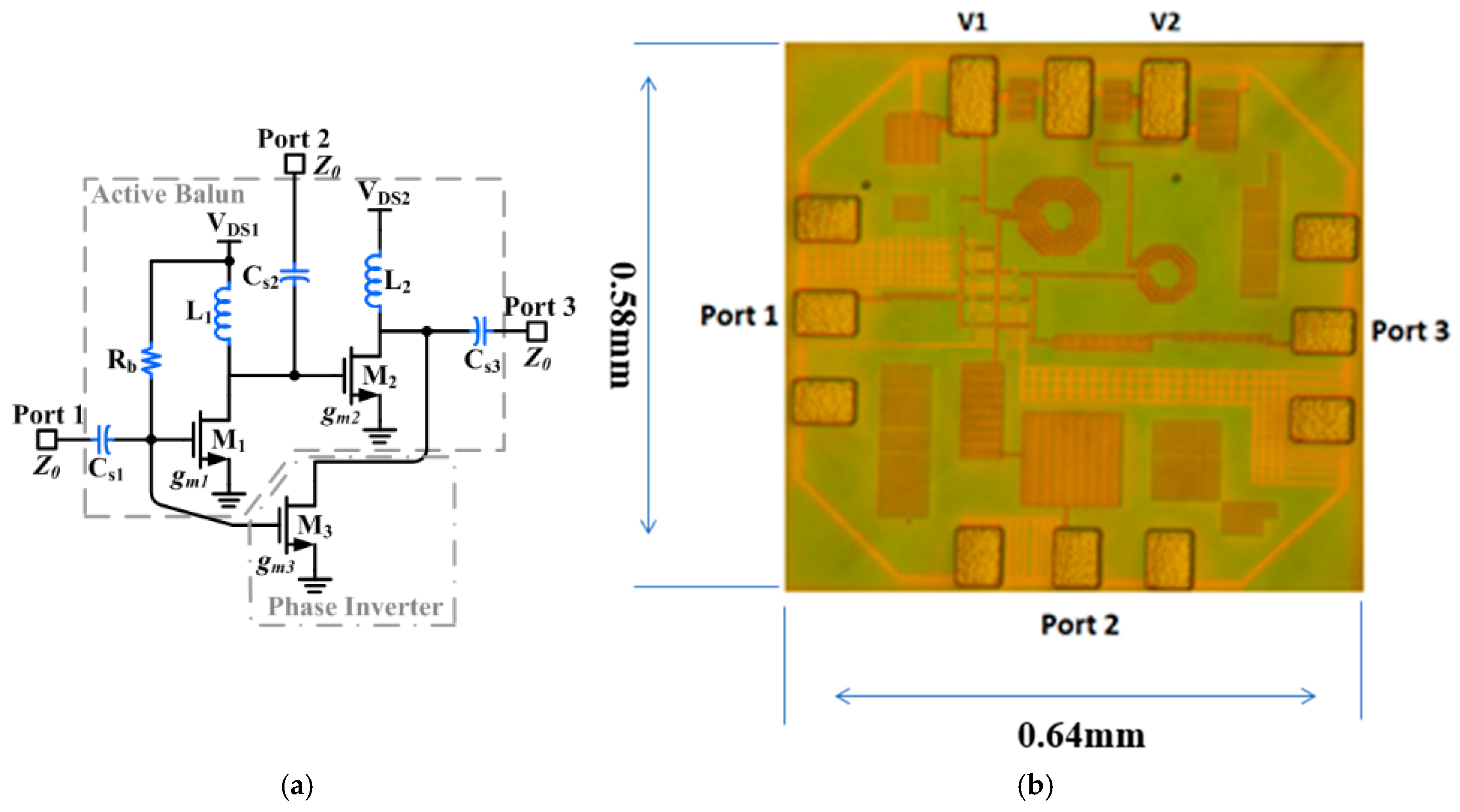
The quasi-circulator was fabricated by TSMC 90 nm 1P9M CMOS technology.
Figure 7a shows a schematic of the quasi-circulator.
Table 1 provides a detailed account of the intricate circuit’s specifications: The M1 assembly employed a ten-finger nMOS device with a gate width of 3 µm. The twenty-finger nMOS device, with a gate width of 2 µm, was used for M2. The M3 implementation involved the use of an nMOS device with forty-three fingers and a gate width of three micrometers. To maintain amplitude balance and input matching for port 1 across a wide operating bandwidth, the drain voltages (VDS1, VDS2) have been adjusted to 0.5 V and 1 V, respectively. The resistor Rb (3.5 KΩ), the drain inductor L1 (2 nH), and the drain inductor L2 (3.6 nH) were all adjusted to ensure optimal matching. The capacitors CS1, CS2, and CS3, with capacitance values of 0.289 pF, 0.45 pF, and 0.3 pF correspondingly, served as the DC-blocking capacitors for ports 1, 2, and 3.
Figure 7b shows the photograph of the chip. The chip’s dimensions are 0.64 × 0.58 mm
2, including the testing pads. For the fabrication of the proposed quasi-circulator, three nMOSFETs with fT values above 142 GHz were employed. In order to achieve wideband performance and smooth gain flatness, an active balun with a cascading structure was chosen. Phase cancellation is a technique that can be used to isolate the suggested quasi-circulator. The reverse phase path is enabled by the CS FET. By employing criteria, an iterative electromagnetic simulation, and a TSMC kit, it is feasible to adjust the dimensions of the practical FET and the circuit characteristics to achieve exceptional performance. In order to assess the parasitic impact, an ADS RF momentum was employed to model the passive components, such as resistors, capacitors, and inductors.
3. Results
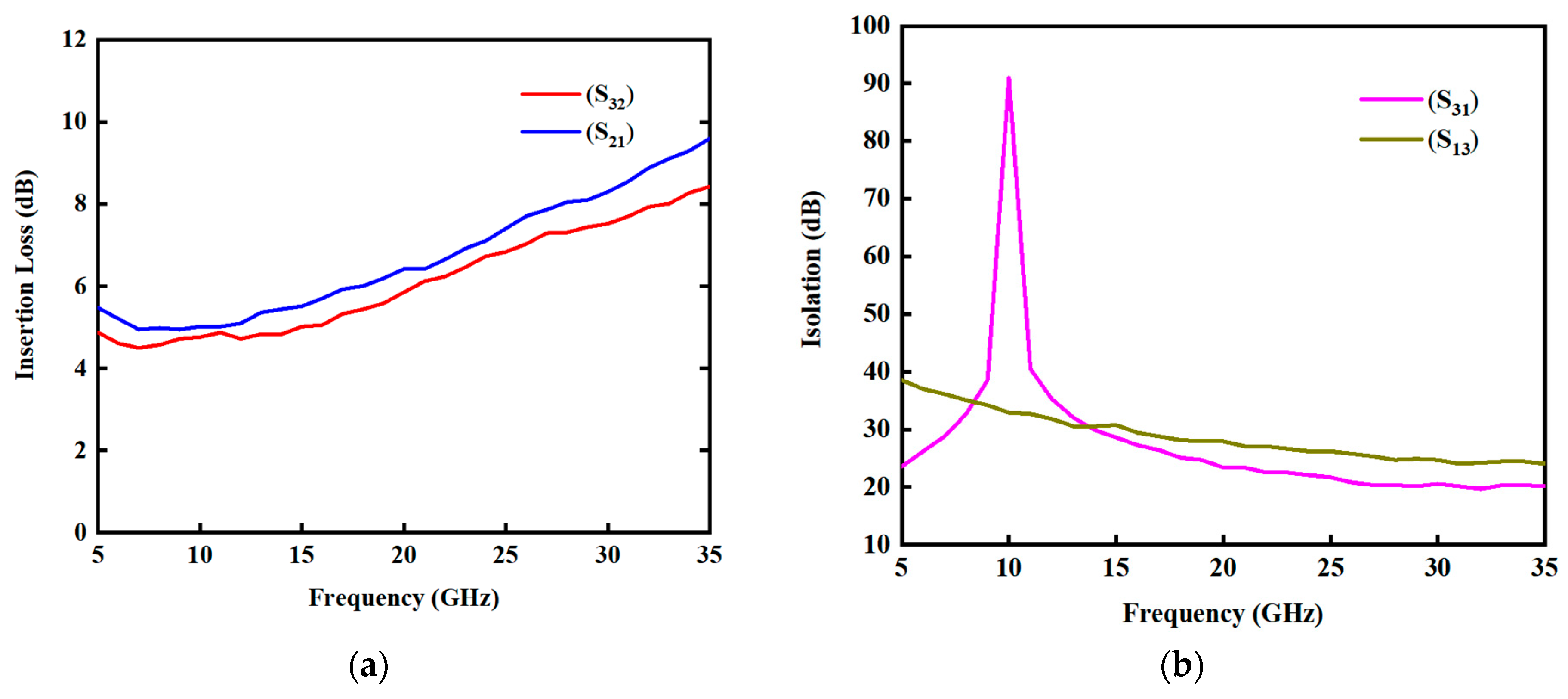
In the case of Vds1, the bias condition is 0.5 V with a current of 71.1 mA, while the bias requirement for Vds2 is 1 V with a current of 5.7 mA. The overall power consumption came to 41.25 milliwatts. As functions of frequency, the insertion loss of the quasi-circulator is depicted in
Figure 8a, which displays the measured values. S21 is around 4.8 to 10 dB, and S32 is approximately 3.4 to 9.1 dB. Based on the results of the simulation, the amplitude imbalance is found to be within the range of 1.5 dB. On the other hand, the result that was measured displays a greater deviation, which can be attributed to the excessively high
gm1 transconductance. It can be observed from the figure that the simulation results of insertion loss are basically consistent with the measured results. The isolations of S31 and S13 are shown as a function of frequency in the range of 5 to 35 GHz in
Figure 8b. These isolations were measured individually. Measured results show |S31| is around 35–55 dB, and |S13|is approximately 40–60 dB. There are some differences between the measured results and the simulation results, which may be caused by the parasitic capacitance of the internal circuit. Due to the fact that it is located in the forward path of the signal flow, high |S31| isolation is often the most difficult to achieve in the active quasi-circulator design. By adjusting the dimensions of the M3 FET, the phase cancellation approach is able to provide superior isolation of the S31 band while maintaining broadband operation.
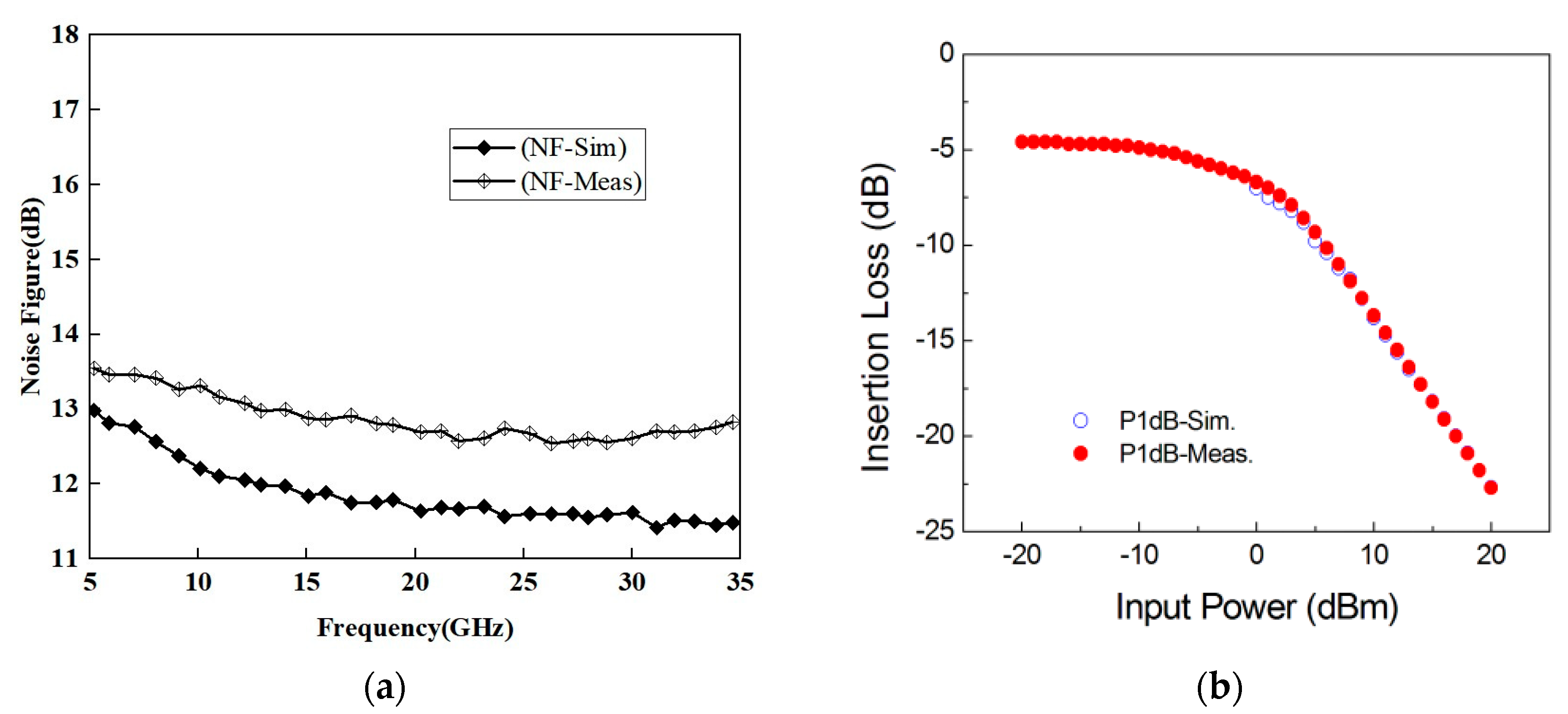
As can be seen in
Figure 9, the measured NF in the 5–35 GHz band falls somewhere between 13 and 14 decibels, which is approximately 1 decibel higher than the simulation. At a frequency of 15 GHz, the simulated result of the input power 1 dB compression point (IP1dB) is 2.8 dBm, while the measured result is 3 dBm from port 1 to port 2. There is a significant degree of concordance between the outcomes of the simulation and those of the experiment.
The performance of the suggested quasi-circulator is compared with the performance of previous quasi-circulators that have been described [
9,
11,
12,
13,
14]. The results are summarized in
Table 2. It is possible for the quasi-circulator that has been designed to offer an extremely broad bandwidth of 28 GHz (147%). All of the insertion losses are lower than 10 decibels, and the isolation of the S31 signal that was produced is higher than 35 decibels. Not only does the proposed quasi-circulator have good port-to-port isolations, but it also maintains wideband functioning while maintaining a compact size. This is in comparison to the data that were presented.


