Article

Continuous Wave Mode Test of Conduction-Cooled Nb3Sn Radio Frequency Superconducting Cavities at Peking University

1
State Key Laboratory of Nuclear Physics and Technology, School of Physics, Peking University, Beijing 100871, China
2
Guangdong Institute of Laser Plasma Accelerator Technology, Guangzhou 510445, China
*
Author to whom correspondence should be addressed.
Appl. Sci. 2024, 14(14), 6350; https://doi.org/10.3390/app14146350
Submission received: 27 June 2024 / Revised: 17 July 2024 / Accepted: 19 July 2024 / Published: 21 July 2024

Abstract

A liquid helium-free cryostat for radio frequency (RF) test of the superconducting cavity is designed and constructed. Gifford-Mcmahon (G-M) cryocoolers are used to provide cooling capacity, and the heat leakage at 4 K is less than 0.02 W. Vertical and horizontal tests of two Nb3Sn cavities are carried out in the cryostat with different surface treatments outside the cavities. Both of the cavities achieve stable continuous wave (CW) operation. A novel treatment, which cold-sprayed a 3.5 mm thick Cu layer onto the outside of the cavity, enables the maintenance of an average temperature of 5.5 K in the cavity at a RF loss of 10 W, implying that the thermal stability and uniformity of the cavity has been significantly improved. Through the synergistic control of four metal film resistors, a cooling rate of 0.06 K/min near 18 K is realized, and the cavity temperature gradient is reduced to 0.17 K/m, which effectively improves the RF performance of the cavity. The maximum E a c c of the cavity reaches 3.42 MV/m, and the Q 0 is 1.1 × 10⁹. An electromagnetic–thermal coupling simulation model for the superconducting cavity is established and is in good agreement with the experimental results. The simulation results show that the cavity with a Cu-spraying treatment and the thermal links of 5N Al can satisfy the E a c c of 10 MV/m under conduction cooling.

1. Introduction

Electron beams are widely used in industry, for applications including environmental remediation, sludge and biosolids treatment, wastewater treatment, production of medical isotopes, additive manufacturing, etc. These processes typically require MeV-scale (1 to tens of MeV) and MW-scale (0.1 to tens of MW) electron beams [1,2,3]. Particle accelerators are one of the primary methods used to generate such electron beams. Superconducting radio frequency (SRF) technology is widely used in modern particle accelerators [4,5,6,7,8] because of its higher efficiency compared to normal-conducting RF technology. By producing higher energy and higher power electron beams, SRF technology demonstrates cost and efficiency advantages over normal-conducting RF technology in these application areas [9,10]. High-purity niobium (SRF grade, residual resistance ratio (RRR) > 300) superconducting cavities are key components in SRF accelerator systems. Traditionally, L-band SRF cavities are immersed in liquid helium (LHe) at 2 K and often equipped with complex helium liquefaction systems. However, commercial cryocoolers present a promising alternative for cooling superconducting cavities. Cryocoolers are easy to operate, highly reliable, and low-cost, making them suitable for replacing the helium liquefaction system in industrial settings. Nevertheless, the cooling capacity of the cryocooler is limited, which requires a higher Q 0 for the superconducting cavities. In recent years, Nb3Sn has been developed as a promising alternative material for superconducting cavities, offering the potential for higher Q 0 and E a c c compared to Nb cavities [11]. The critical temperature ( T c ) of Nb3Sn is almost twice that of Nb. The surface resistance ( R s ) of Nb3Sn at 4 K is of the same order of magnitude as that of Nb at 2 K. This implies that the Nb3Sn film cavity can operate at 4 K or even higher temperatures, making it possible to cool the superconducting cavity by thermal conduction using commercial cryocoolers.
A vapor diffusion method has been under development since the 1970s [12,13,14] and is the most effective method to prepare Nb3Sn film for a Nb cavity. The institutions that have worked on Nb3Sn SRF cavities include Cornell University (New York, NY, USA) [15,16,17], Fermi National Accelerator Laboratory (FNAL, Batavia, IL, USA) [18], the Thomas Jefferson National Accelerator Facility (Jefferson Lab, Newport News, VA, USA) [11], the Institute of Modern Physics (IMP, Lanzhou, China) [19,20], the Institute of High Energy Physics (IHEP, Beijing, China) [21], Shanghai Advanced Research Institute (SARI, Shanghai, China) [22], Peking University (PKU, Beijing, China) [23], the High Energy Accelerator Research Organization (KEK, Tsukuba, Japan) [24], etc. FNAL fabricated high-performance Nb3Sn cavities with different frequencies. The 1.3 GHz single-cell cavity coated in FNAL reached a maximum E a c c of 24 MV/m when tested in 4.4 K LHe, and Q 0 remained above 1 × 10¹⁰ at an E a c c of 20 MV/m [18]. Conduction-cooled single-cell SRF cavities at different frequencies have been demonstrated over the past few years. Researchers at FNAL, JLab, and Cornell University used different types of cryocoolers and methods to connect the cryocooler’s 4 K stage to the cavity, achieving CW operation of the superconducting cavity at 650 MHz [25], 952.6 MHz [26], 1.5 GHz [27], and 2.6 GHz [28]. G. Ciovati [26] et al. reported an E a c c of 12.4 MV/m on a multi-metallic single-cell prototype Nb3Sn cavity, which represents the highest E a c c achieved to date in a conduction-cooled superconducting cavity. Simultaneously, the Q 0 has also reached 1 × 10¹⁰ or higher, meeting the needs of industrial applications. Accordingly, the compact accelerators based on conduction-cooled Nb3Sn cavities for applications such as wastewater treatment have been concurrently developed [29,30,31].
In this paper, we present the development of a LHe-free cryostat for RF testing of superconducting cavities, which can also be used for other potential studies [32]. The residual magnetic field and temperature distribution inside the cryostat are simulated. The RF test results of an NS04 Nb3Sn cavity clamped with an oxygen-free copper (OFC) hoop and of an NS03 Nb3Sn cavity coated with Cu on the outer surface are introduced. The electromagnetic and thermal coupling simulation of the Nb3Sn cavity is carried out, and the experimental and simulation results are analyzed and discussed.

2. Experimental Descriptions

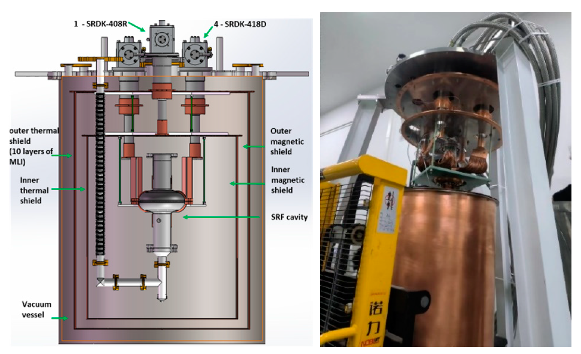
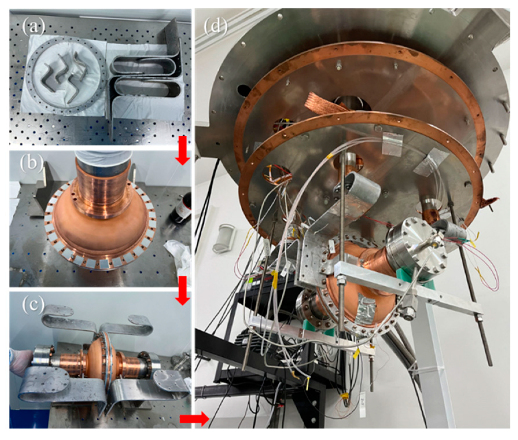
2.1. Cryostat Design

We designed and constructed a set of LHe-free cryostats which can perform vertical and horizontal testing of superconducting cavities. Figure 1 shows the picture of the cryostat. Five G-M cryocoolers manufactured by the Sumitomo Corporation are installed on top of the cryostat, including four 4 K cryocoolers (SRDK-418D, 1.8 W at 4.2 K) and one 10 K cryocooler (SRDK-408R, 5.4 W at 10 K). To reduce heat leakage at 4 K, two thermal shields made by OFC are designed, which are cooled by two stages of the 10 K cryocooler. Two shields are respectively suspended on the top plate of the cryostat by four garolite rods, and the side and bottom of the outer thermal shield are wrapped with 10 layers of multi-layer insulation (MLI). Two magnetic shields are designed to reduce the residual magnetic field in the cavity area and are placed inside the two thermal shields, respectively. The superconducting cavity is mounted on a garolite base that hangs from the top of the inner thermal shield via four titanium rods. A total of 13 silicon diode thermometers (DT-670-CU, Lake Shore Cryotronics, Westerville, OH, USA) are installed in the cryostat to measure the temperature of the cavity and other locations. RF power is coupled into and out of the cavity via two RF cables. The cryostat is equipped with a dry scroll pump (nXDS10i, Edwards China, Shanghai, China), a turbomolecular pump (nEXT240D, Edwards China, Shanghai, China), and a wide-range vacuum gauge (WRG-S, Edwards China, Shanghai, China). In the test of the NS03 cavity (Part 4), 3 cryogenic flux-gate magnetometers were installed inside the cryostat to monitor the magnetic field variations, and four heaters were also installed to control the cooling rate of the cavity.

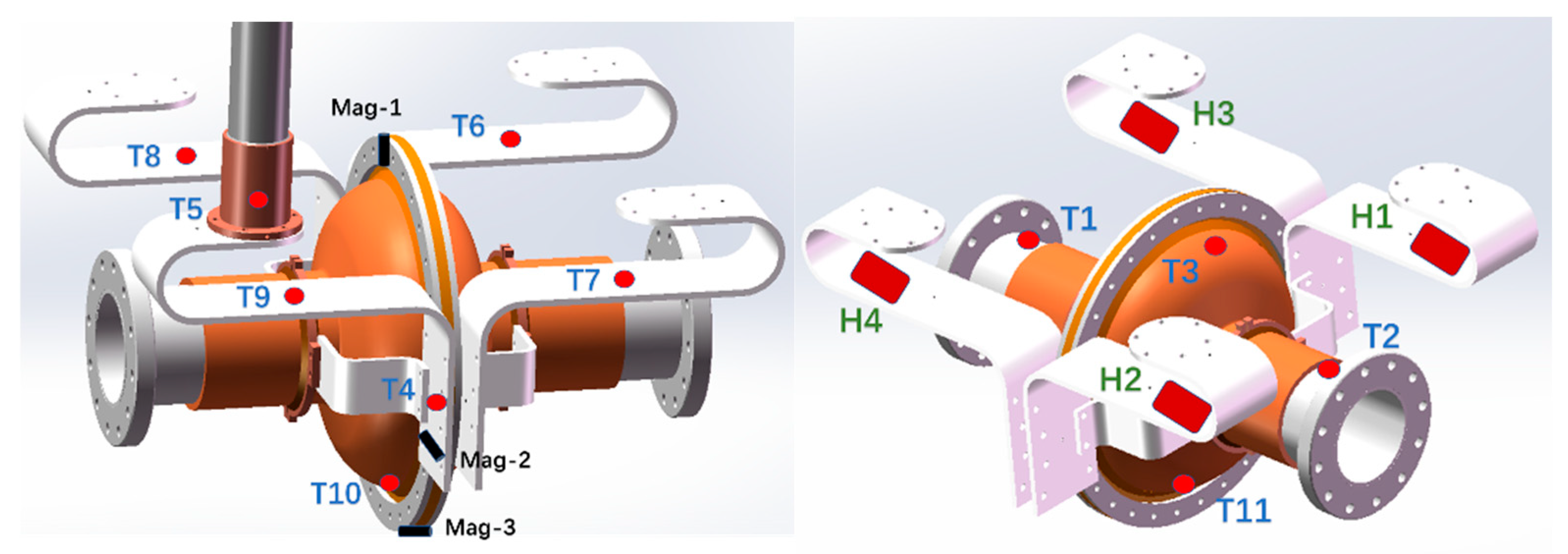
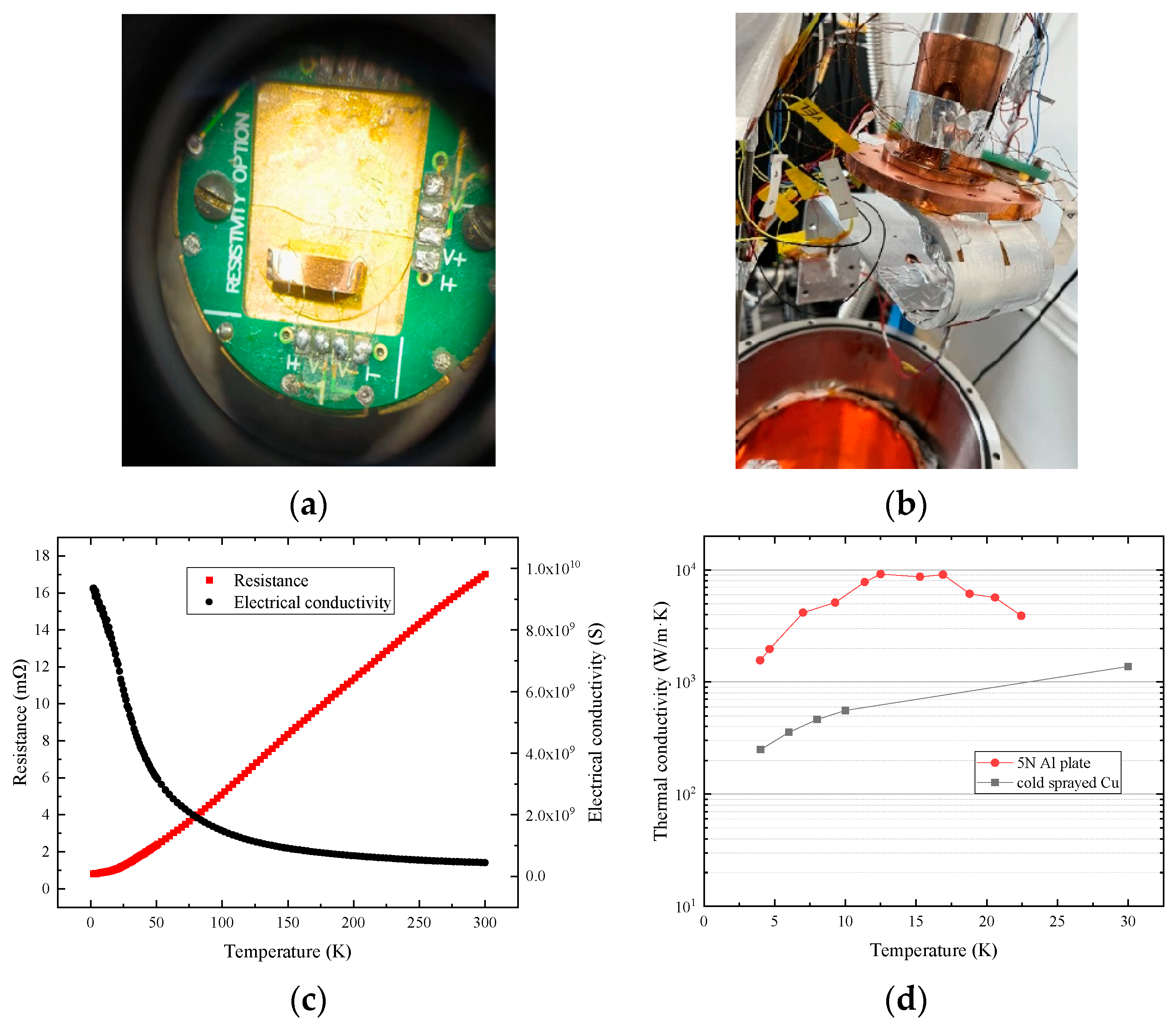
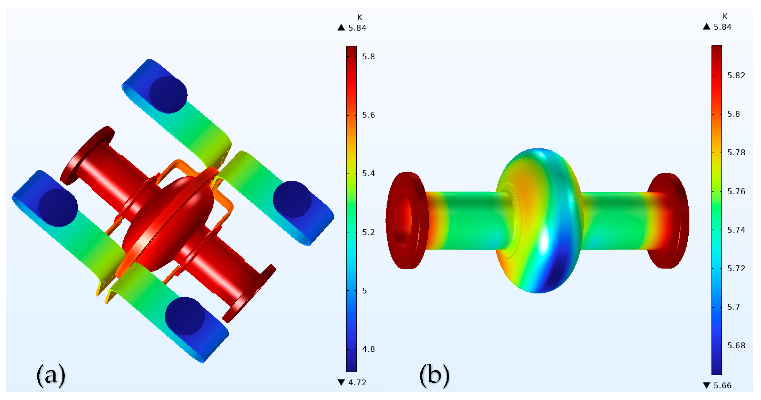
2.1.1. Temperature Distribution and Heat Leakage Calculations

To minimize heat leakage at 4 K, we employed COMSOL Multiphysics® (COMSOL Co., Ltd., Beijing, China) to simulate the temperature distribution and heat leakage of the cryostat. We conducted a temperature simulation of the two thermal shields. Although the surfaces of the thermal shields were polished, they had oxidized at the time of installation, so we set the emissivity of the surfaces without MLI to 0.2, and that of the surface with MLI to 0.005. The RRR of Cu used in the simulation is 100. The variation in thermal conductivity and cooling capacity with temperature was taken into account in the simulation. Figure 2 presents the simulation results of the temperature distribution of the two thermal shields. The outer and inner thermal shields operated at approximately 50 K and 7 K, respectively, with temperature differences of less than 6 K and 1 K across each shield. The radiant heat leakage of the two thermal shields was 42.407 W and 0.393 W. Since the top plate of the outer shield was not covered with MLI, the radiant heat leakage contributed about 70% of the total radiant heat leakage. Table 1 summarizes the heat leakage in each temperature zone of the cryostat. The total heat leakage at 4 K was estimated to be less than 0.02 W.

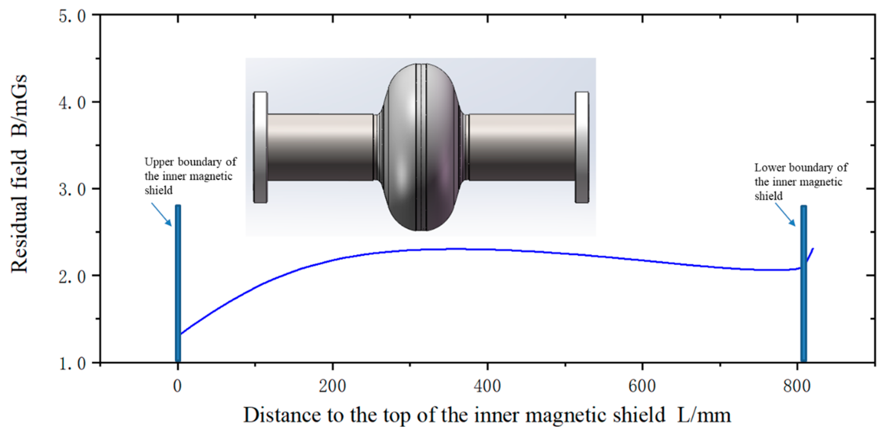
2.1.2. Residual Magnetic Field Simulation

The high ambient magnetic field at the location of the superconducting cavity can significantly decrease the RF performance of the cavity significantly. Equation (1) [33] provides the additional surface resistance R m a g due to the cavity-trapped magnetic field, where B e x t represents the trapped field, B c 2 denotes the upper critical field, and R n is the normal state surface resistance. For conventionally processed 1.3 GHz Nb cavities, B c 2 = 240   m T , R n = 1.7   m Ω , a n d   R m a g = 0.35 × B e x t m G   n Ω [33], as follows:
R m a g = B e x t 2 B c 2 R n
The trapped magnetic field is positively correlated with the ambient magnetic field. To address this issue, two magnetic shields were designed for the cryostat, and the material was permalloy 1J79. Figure 3 presents the simulation results of the environmental magnetic field at the axis of the superconducting cavity using CST Studio Suite® (Dassault Systemes, Pairs, France). The maximum magnetic field is 2.4 mG, and the environmental magnetic field on the surface of the superconducting cavity is consistently lower than this value. If the ambient magnetic field of 2.4 mG is fully trapped by the Nb cavity, the resulting additional R s is 0.84 nΩ, which does not significantly affect the performance of the superconducting cavities. In the experiments, the magnetic fields monitored by the three magnetometers were sometimes higher than this value, due to the additional dynamic ambient magnetic field generated when cooling down or turning on the heaters.

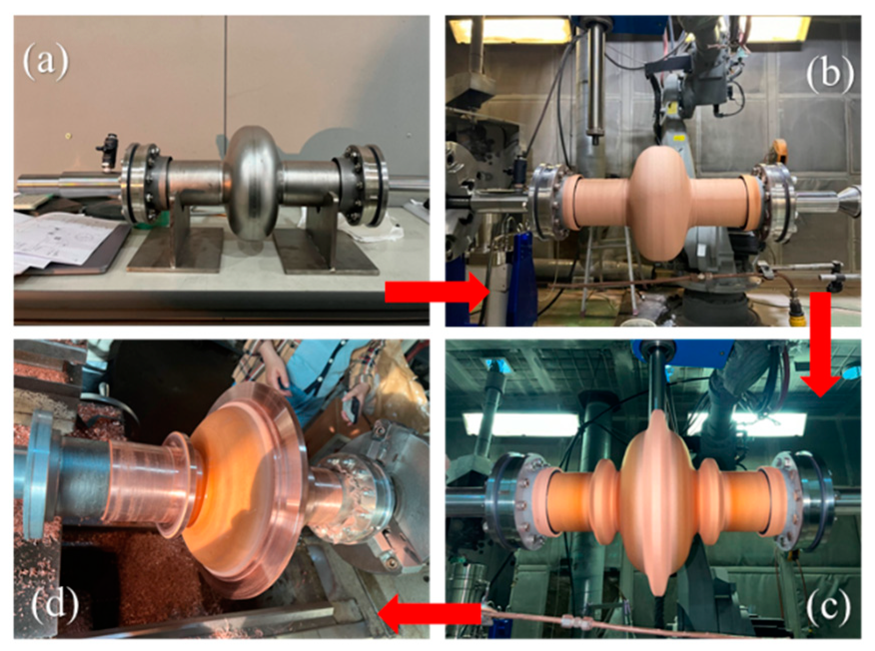
2.2. Superconducting Cavities Treatment

2.2.1. Nb3Sn Inner Coating

Two 1.3 GHz TESLA-type single-cell Nb cavities (2.6 mm thickness, RRR > 300), numbered NS04 and NS03, were used for experiments in this paper. Nb3Sn thin films were successfully prepared on the inner surface of the two cavities using tin vapor diffusion. Prior to the deposition, the Nb cavities were treated with buffered chemical polishing (BCP) and high-pressure water rinsing (HPR). Three evaporation boats made of tungsten were placed at different heights along the center axis inside the superconducting cavity with different weights of tin, supported by fine Nb wires. The nucleating agent SnCl2 was placed in a tungsten crucible with an independent heater. The cavities were placed in a high-temperature vacuum furnace and were heated to different temperatures to undergo nucleation, coating, and annealing processes. The specific process parameters are shown in Table 2. The results of the vertical test in LHe are shown in Figure 4. The maximum E a c c reached 17.3 MV/m for the NS04 cavity and Q 0 exceeded 1.1 × 10¹⁰ at low E a c c for the NS03 cavity.

2.2.2. Surface Treatment outside the NS04 Cavity

Two separate experiments were conducted using NS04 and NS03, each with distinct treatments applied to the outer surface of the superconducting cavities.
For the NS04 cavity, OFC hoops and straps were used to connect the cryocooler’s 4 K stage to the cavity, as illustrated in Figure 5. Four Cu hoops were wrapped around the ellipsoidal section, while two additional hoops were clamped to the upper and lower beam tubes, respectively. Figure 5b shows the actual hoops and straps. To mitigate the pressure on the cavity caused by the contraction of the hoops, the straps were unrolled and padded between the hoops and the cavity. The cavity was mounted vertically on the G-10 base in the cryostat, and then we performed the RF test after turning on the cryocoolers to cool it down, as detailed in Part 3.

2.2.3. Surface Treatment outside the NS03 Cavity

The relatively low E a c c achieved in NS04 cavity tests was primarily attributed to insufficient thermal stability and thermal uniformity, which is presented in Section 3.1. To solve this problem, a cold spraying technique was used to deposit a 3.5 mm thick Cu layer on the outer surface of NS03 cavity. Cold spraying is capable of creating a bond between Nb and Cu with a strength exceeding 40 MPa. In order to guarantee the bonding and to avoid deformation of the cavity, instead of sandblasting, we first cold sprayed a Cu base layer of 300 μm with He gas. Subsequently, a Cu layer of about 3.2 mm was deposited in eight passes using N2, and three flanges were sprayed at the equator and near the irises to facilitate the connection with the Al plate. The powder used for spraying was 99.95% pure, spherical Cu powder with a particle size of 15–40 μm. Prior to spraying, the cavity was sealed with an adhesive ring and the interior was filled with 0.12 MPa Ar gas to protect the Nb3Sn film. During the spraying process, we used N2 to cool the cavity, in order not to exceed 100 °C so we could minimize the oxidation of the Cu layer and the effect on the Nb3Sn film. All deposition processes were finished in 1 day. The cavity was then machined; Figure 6 shows the deposition and machining processes.
In the NS03 cavity test, we used high-purity Al (purity > 99.999%, 5N) plates with a high thermal conductivity instead of OFC straps. Four Al plates were used to connect the cavity to the cryocoolers and were bent in a C-shape to reduce vibration transfer from the cryocoolers. Two 5N Al rings were assembled on both sides of the equatorial Cu flange to enhance the circumferential heat conduction of the superconducting cavity, and the equatorial flange was also connected to the beam tube flanges with 5N Al plates to increase the axial heat conduction. The connections were all connected using 316 L screws, spacers, and silicon bronze nuts, and 0.1 mm thick indium foils were padded on the contact surface. The preloading force of the bolts was 10 N·m. Apiezon N grease was applied to the contact surface between the Al plates and the cryocoolers, and indium foils were not used to enable easy disassembly. After the machining process, the cavity was ultrasonically cleaned with anhydrous ethanol, and subjected to HPR in a class 100 clean room. Indium wire with a 2 mm diameter was used to seal the cavity with 316 L flanges, which was then pumped to 8 × 10⁻⁵ Pa vacuum. The installation of the 5N Al thermal links was then completed in the clean room. The cavity was then mounted in the cryostat for a horizontal test. In this cryostat, a horizontal test allows for shorter thermal links, which facilitates enhanced thermal conduction. Figure 7 shows the installation of the cavity in a clean room and its placement in the cryostat. Eleven thermometers were mounted on the cavity, thermal links, and 2nd stage of one cryocooler. Three mutually orthogonal cryogenic flux-gate magnetometers were arranged at different positions on the equator of the cavity. Four heaters (metal film resistors) were installed on the thermal connections. Figure 8 shows the approximate mounting location of the thermometers, magnetometers, and heaters.
We tested the mechanical properties and thermal conductivity of cold sprayed Cu. We fabricated three samples with a 2 mm thick Cu layer cold sprayed with N2 on a Nb substrate and tested the bond strength between Nb and Cu using a tensile method. The average bond strength reached more than 58.4 MPa, and fracture occurred at the glue bond rather than between Nb and Cu. Figure 9 shows a metallographic sample of the Nb–Cu bonding interface and the bond strength test results of the three samples. We also carried out Scanning Electron Microscope (SEM) measurements on the morphology of the sprayed Cu, and the Cu particles underwent obvious plastic deformation, which implies a good bonding force. The Cu-coated cavity was cooled down to 4 K and heated up to 300 K without any peeling or cracking of the coating. Figure 10 shows the SEM image of the sprayed Cu.
The electrical and thermal conductivity of the sprayed Cu were measured using a physical property measurement system (PPMS, Quantum Design). Cu samples were sprayed with 99.9% pure Cu powder and were stripped and cut into rectangular pieces, placed on a sample stage, and cooled down from room temperature to 4 K after making electrodes, and the electrical conductivity was measured during the cooling process. Similarly, thermal conductivity measurements were made at several selected temperature points during the cooling process, and 20 measurements were taken at each temperature point and averaged. The residual resistivity ratio (RRR) for 300 K–4 K, calculated using electrical conductivity, was 21. The thermal conductivity of Cu at 4 K was 249.6 W/(m·K), three times that of Nb. Figure 11 shows the installation of the samples with the measurement results of electrical and thermal conductivity. At 4 K, 5N Al has a high thermal conductivity [34], making it ideal for manufacturing thermal links for superconducting cavity conduction cooling. We measured the thermal conductivity of the Al plates used in the experiments using the “two heater” method [35,36], which exceeded 1500 W/(m·K) at 4 K. Figure 11b shows the installation for thermal conductivity measuring of Al plates, and Figure 11d contains the results of the measurements.

3. Results Analysis

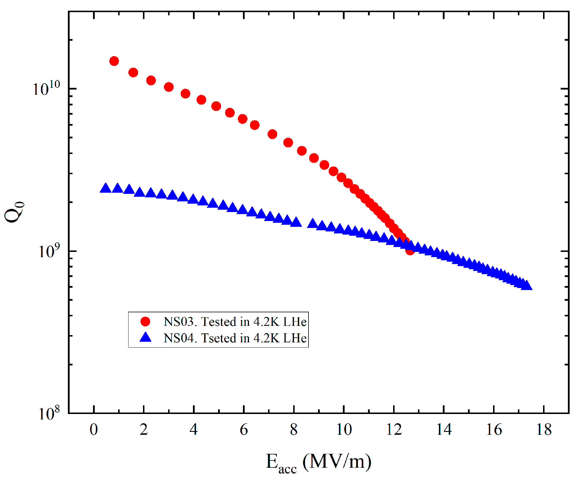
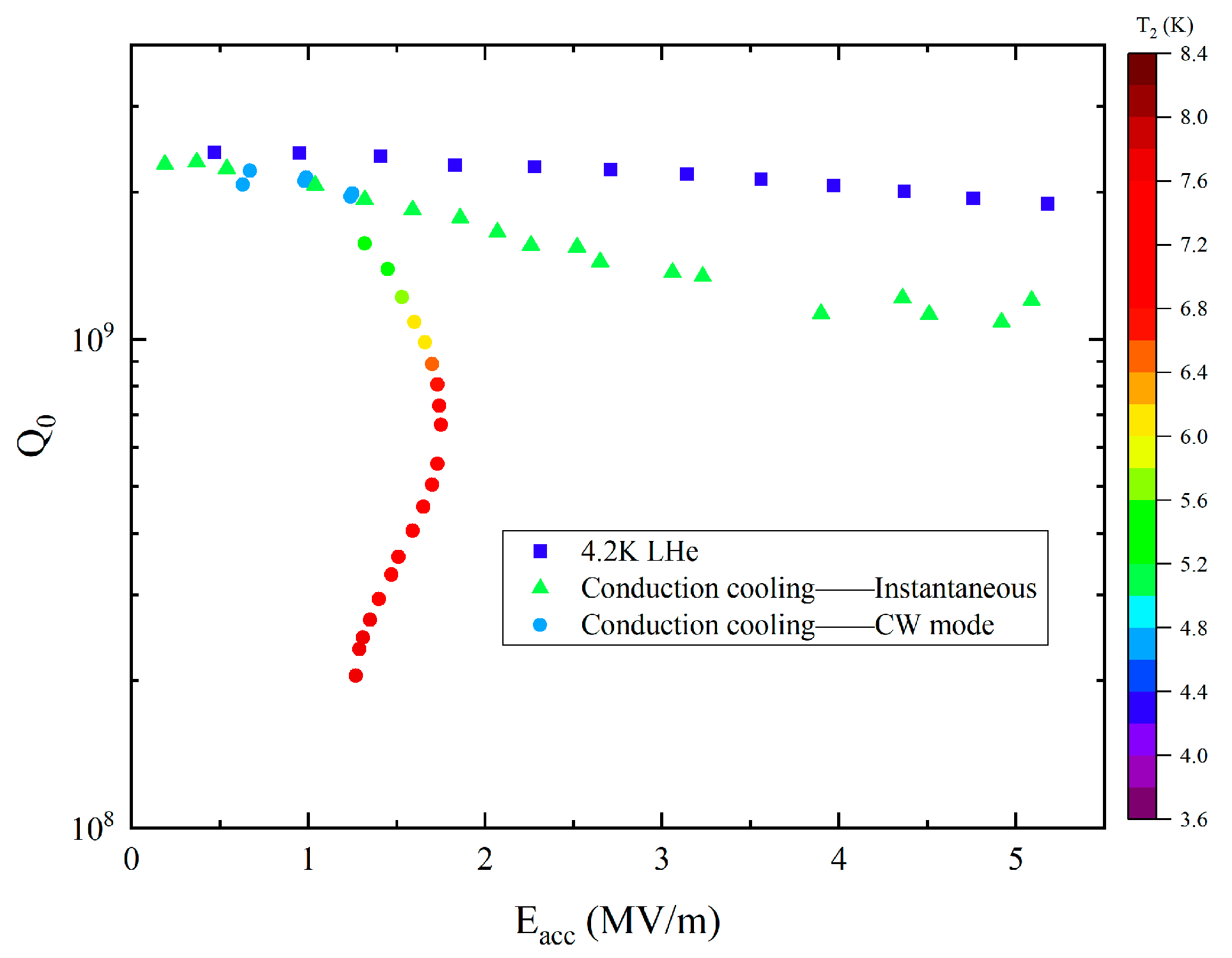
3.1. NS04 Cavity Test Results

In the first test, a total of approximately 100 h of cooling was performed, and the vacuum in the cryostat was as low as 1 × 10⁻⁷ Pa at low temperatures. The end of the beam tube was cooled down to about 5.4 K ( T 1 ), and the ellipsoidal portion was cooled down to 4.0 K ( T 2 ). During the initial RF test, the cavity temperature rose fast after loading RF power, so we collected data points when adding instantaneous power. The average temperature ( T a v g = ( T 1 + T 2 ) / 2 ) of the cavity was cooled to 5 K before each power load, and Q 0 and E a c c were measured immediately after loading power, followed by power shutdown. When the cavity was re-cooled to 5 K, the power was increased and the above operation was repeated. Due to power limitations, the maximum instantaneous E a c c measured during the test was 5.09 MV/m and the instantaneous Q 0 was 1.2 × 10⁹. After reaching the maximum transient E a c c , the power loading was maintained and the cavity temperature was finally stabilized at 9 K for T 1 and 6 K for T 2 , at which time E a c c was 1.25 MV/m and Q 0 was 2.1 × 10⁸, and the RF loss in the cavity ( P l ) was 0.936 W. The cavity was operated for more than 10 min at this operating point.
After the test, a temperature cycle through T c was performed by turning off the cryocoolers until T 1 and T 2 exceeded 25 K. Then, the cryocoolers were power-cycled on and off to slowly lower the cavity temperature to 17 K, below which the cryocoolers were kept on. The cavity was cooled to the base temperature, with T 1 = 5.4   K , T 2 = 4.0   K . During this cooling process, the thermal gradient at either side of the equator along the axial direction of the cavity temperature at 17–19 K was reduced from the original ~40 K/m to 12 K/m. A subsequent RF test in CW mode was performed, which involved loading power and waiting for the cavity to thermally equilibrate, followed by a slow increase in power, with each equilibrium point stabilizing for more than 10 min. The E a c c of the cavity reached a maximum value of 1.75 MV/m when the forward power was 1.37 W. At this time, the Q 0 was 6.7 × 10⁸, the P l was 0.573 W, and the T 2 increased to 5.5 K. Continuing to increase the power, the Q 0 decreased rapidly due to the increased temperature of the cavity, and the E a c c decreased as well. When P l was increased to 0.937 W, E a c c and Q 0 reached 1.31 MV/m and 2.3 × 10⁸, respectively, and the T 2 increased to 5.9 K. Figure 12 shows the Q 0 E a c c curves for the NS04 cavity for these two tests, as well as the curve for the vertical test in 4.2 K LHe (for comparison, only test points below 5 MV/m are plotted).

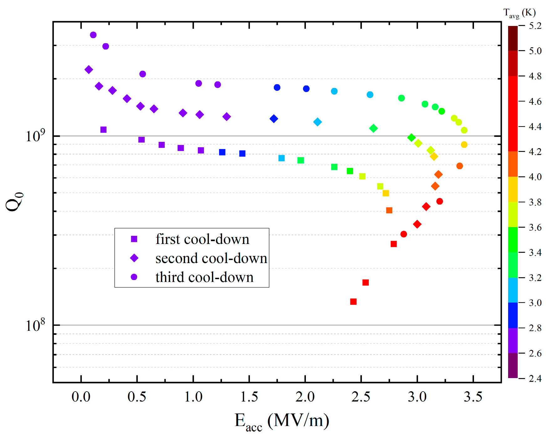
3.2. NS03 Cavity Test Results

The NS03 cavity underwent an RF test after 72 h of cooling. The cavity was cooled to about 2.58 K, with a temperature difference of less than 0.1 K. The ambient magnetic field before cooldown had the following conditions: B x = 14   m G , B y = 1.1   m G , and B z = 1.56   m G . During the cooldown, B m a x reached a maximum of 120 mG due to thermal currents. We performed RF tests in CW mode under three cooling conditions: the first was direct cooling without controlling the cooling rate, the second was two cycles of cooling by switching the cryocoolers on and off between 30 K and 12 K, and the third was the slow control of the cooling rate at 0.06 K/min using the heaters, after the cavity was warmed up to 25 K, with the heaters turned off after cooling down to 15 K. The cavity temperatures and ambient magnetic fields for these three cooling processes are given in Figure 13, and the corresponding cavity surface temperature gradients and ambient magnetic fields at 18 K are given in Table 3. The cavity was cooled to a base temperature of 2.58 K before each RF test, and the measured Q 0 E a c c curves under the three cooling conditions are given in Figure 14, with the points on the graphs being the thermal stability points.
The overall lower measured Q 0 and E a c c may be due to the fact that the film was partially damaged or contaminated during transportation and processing, which will be discussed in Part 5. Nevertheless, a relatively good Q 0 E a c c curve was measured under the third cooling condition. The Q 0 was over 3 × 10⁹ at low E a c c . The E a c c reached a maximum value of 3.42 MV/m when the forward power was loaded to 3.04 W. At this time, the Q 0 was 1.1 × 10⁹, the P l in the cavity was 1.372 W, and the T a v g stabilized at 3.86 K. Continuing to increase forward power, both Q 0 and E a c c showed a decrease.

4. Discussion

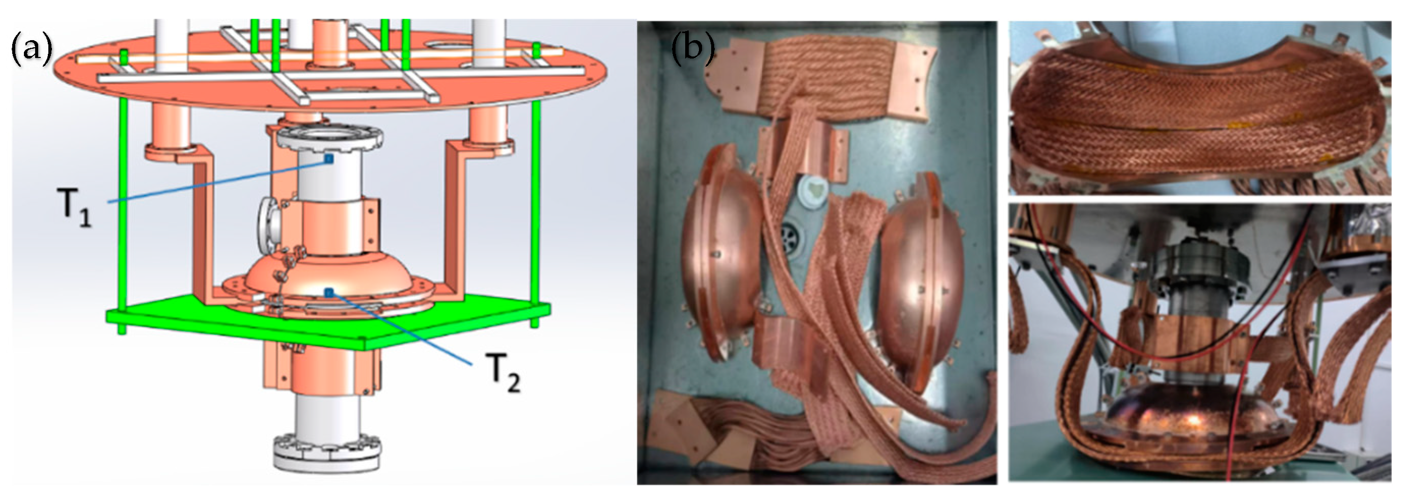
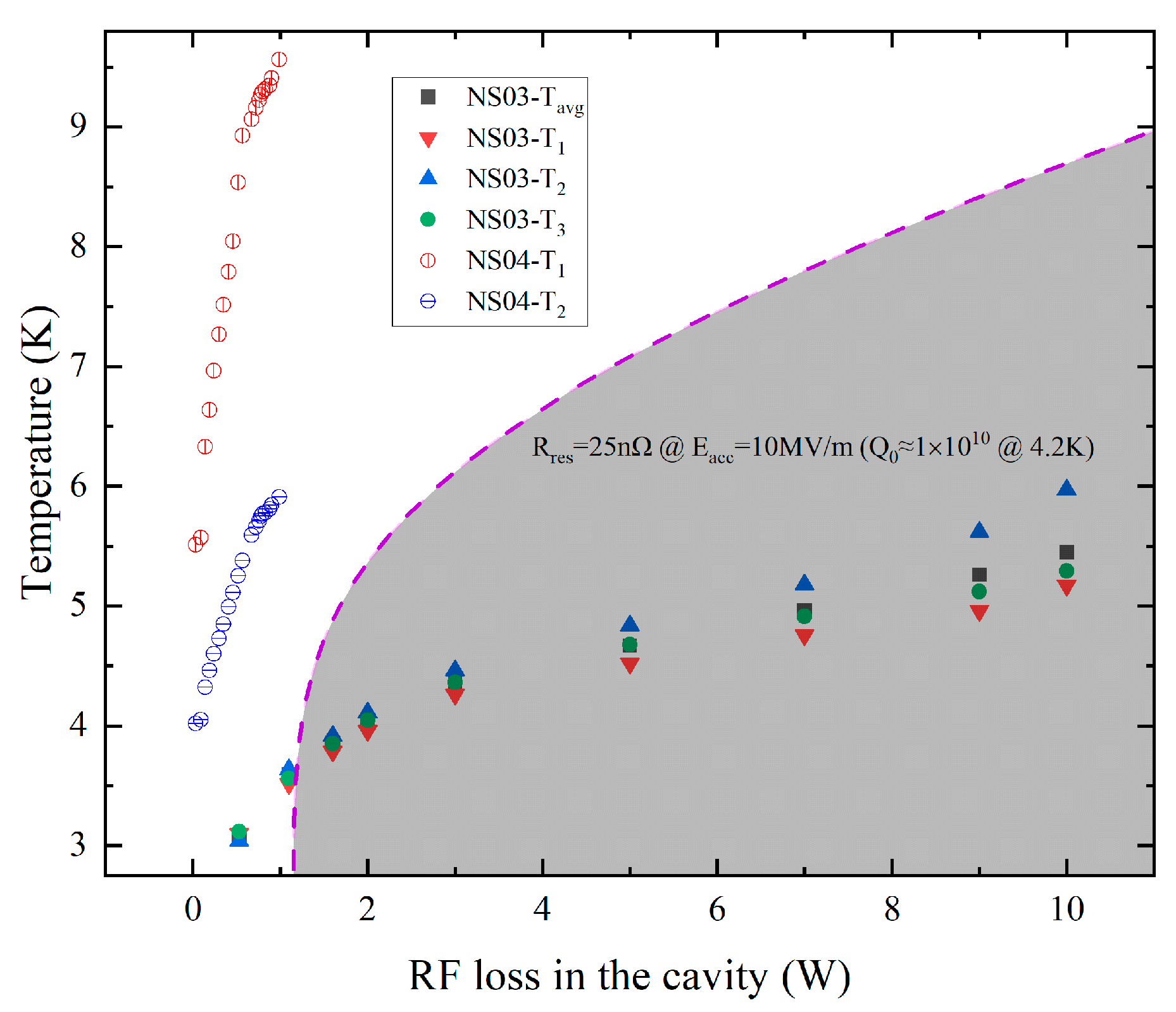
4.1. Thermal Stability and Uniformity

In order to verify the thermal stability and uniformity of the NS03 cavity, we conducted long-time CW tests under different P l conditions, and Figure 15 contains these results, with the points on the graph in steady states. The cavity could be operated stably in CW mode at a P l of at least 10 W. We compared the variation in cavity temperature with P l , and the results are shown in Figure 16. At the same P l , the T a v g of the Cu- clamped cavity is significantly lower and the cavity permitted a larger P l . In addition, as P l increases, the temperature difference ( T d ) between the equator and the end of beam pipe of the NS04 cavity gradually increases, approaching almost 4 K at P l of 1 W. In contrast, the T d of the NS03 cavity could be maintained at around 0.5 K when P l is below 7 W. At a P l of 10 W, the maximum temperature difference in the NS03 cavity was 0.8 K. The shaded area in Figure 16 indicates that the thermal stability of the cavity is sufficient to operate the cavity at 10 MV/m. Cold sprayed Cu treatment distinctly improved the thermal stability and thermal uniformity of the cavity. The P l of the NS03 cavity has a sufficient margin, which indicates that thermal stability is not the main limiting factor for low gradient.

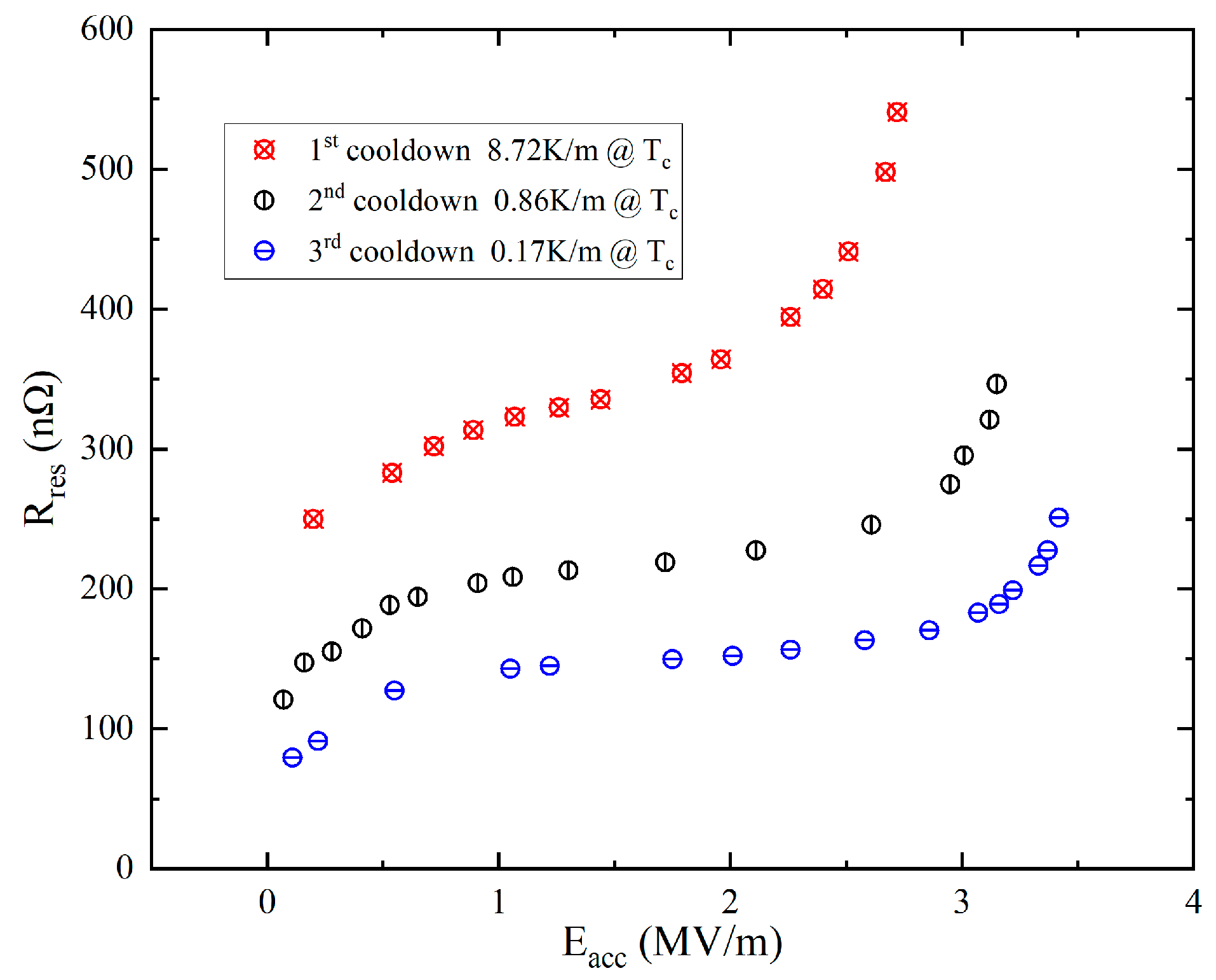
4.2. Effect of Cooling Rate on RF Performance of Nb3Sn Cavity

Minimizing the thermal gradient across the cavity during cooldown, particularly during the superconducting transition, is crucial for optimizing the RF performance of the cavity. Due to the thermoelectric effect, thermal currents will be generated between the Nb/Nb3Sn bimetallic structures, which in turn generates magnetic fields, which may be trapped by the cavity at T c , resulting in an increase in R s and worse cavity performance [37,38] Although this effect is more pronounced at high E a c c , it is also reflected in our experiments. For NS04 cavity, at nearly the same P l (0.936 W and 0.937 W), the E a c c and Q 0 of the Nb3Sn cavity after temperature cycling are slightly higher than those obtained after the initial cooldown. For the NS03 cavity, the surface resistance ( R s ), the BCS surface resistance ( R B C S ), and the residual surface resistance ( R r e s ) were calculated for three cooling conditions. The R s of Nb3Sn cavity can be calculated from the experimental data using Equation (2) [33], where G is the geometric factor of the cavity, and G is 270 for 1.3 GHz TESLA cavity used in the experiment. The theoretical calculation formula of R s is Equation (3) [33], and R B C S is the temperature-dependent BCS resistance, which can be calculated using Equation (4) [33] for a Nb3Sn cavity, where f is the resonant frequency and T is the cavity temperature. The R B C S of the Nb3Sn cavity is 2.6 nΩ and 10 nΩ at 4.2 K and 5 K; R r e s is the main source of R s in the experiment. After subtracting the R B C S , we obtain the curve of R r e s with E a c c , as shown in Figure 16. The controlled slow cooling near the T c reduced the temperature difference over the cavity, resulting in the smaller trapped flux due to the thermal current and lower R r e s , and the performance of the cavity was significantly improved.
Controlling the power of the heaters allows the cavity to have a smaller temperature gradient during cooling, but the current of the heaters increase the ambient magnetic field, which may in turn increase R r e s . Therefore, it is necessary to use heaters with a large resistance in order to reduce the heating current and to rationally arrange the location. In this paper, the heaters were placed in the thermal links away from the cavity instead of on the cavity to minimize the magnetic field generated by the heaters. The magnetometers showed significant increases in the ambient magnetic field when the heaters were used individually, but there was no significant change in the magnetic field when all four heaters were used at the same time, which may be due to the fact that the symmetrical placement of the heaters allowed the generated magnetic fields to cancel each other out, which also allowed the R r e s to be significantly reduced. Overall, this arrangement and use of heaters is effective.
R s = G Q 0
R s = R B C S + R r e s
R B C S = 9.4 × 10 5 f 2 T e 2.2 T c T

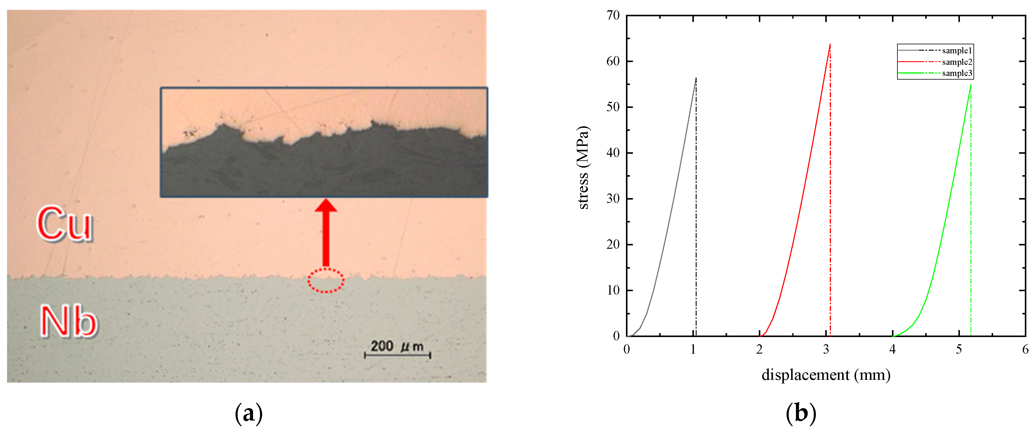
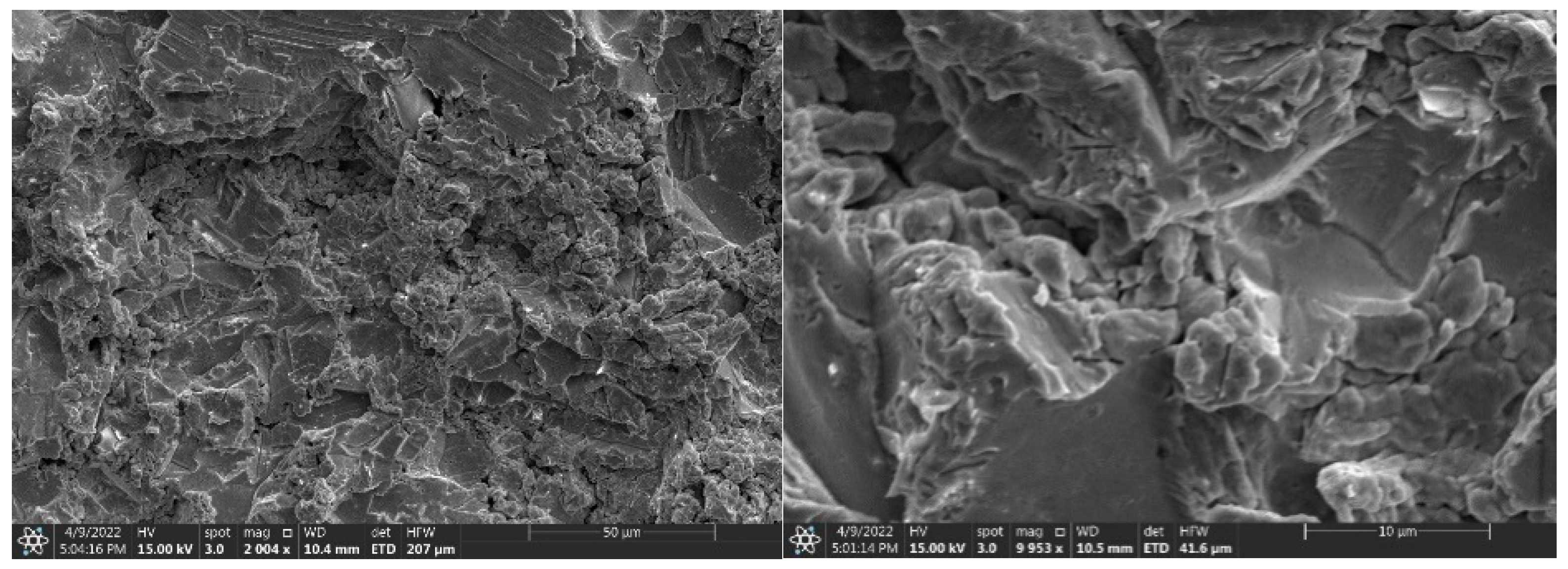
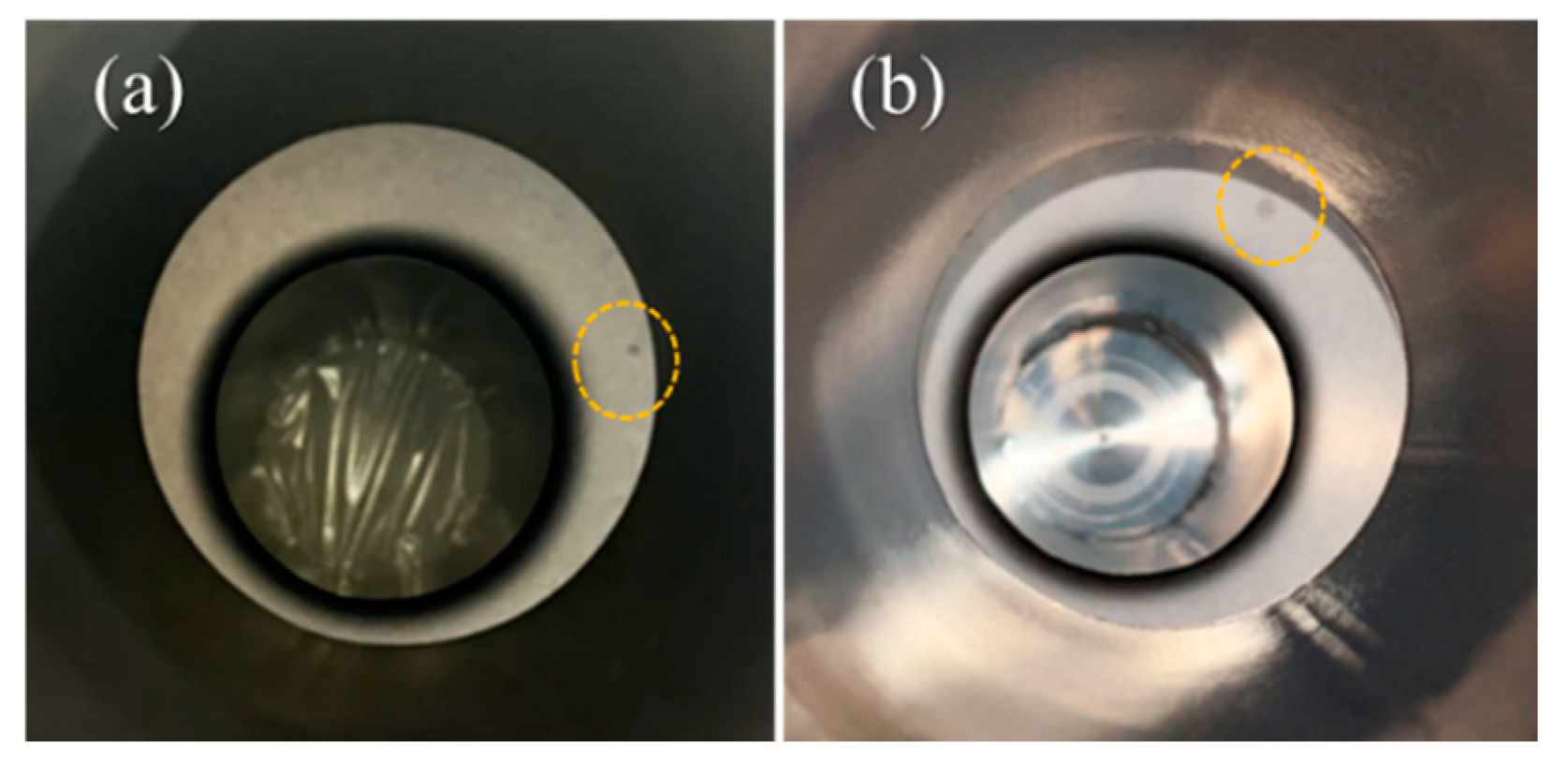
4.3. Causes of Performance Degradation of NS03 Cavity

Obvious degradation of the RF performance under conduction cooling tests of the NS03 cavity was observed. Due to the lack of a clean environment in the cold spray shop and the need to change the clamping tooling, the cavity was exposed to air several times before spraying, resulting in contamination such as oil. Figure 17 shows a visible contamination or defect that was still present in the cavity, despite the HPR treatment prior to testing. This may be the reason that the temperature on the side of the RF test with the defect ( T 2 ) was higher than the other side ( T 1 ). In addition, the cavity is poorly concentric due to multiple high-temperature treatments, and the cavity may have undergone minor deformation during high-speed rotation when processing. Cold shrinkage of the Cu layer at low temperature may also lead to film damage, but according to G. Ciovati’s work [26], this should not be the main reason. Overall, these causes of cavity performance degradation should be avoidable in subsequent experiments.

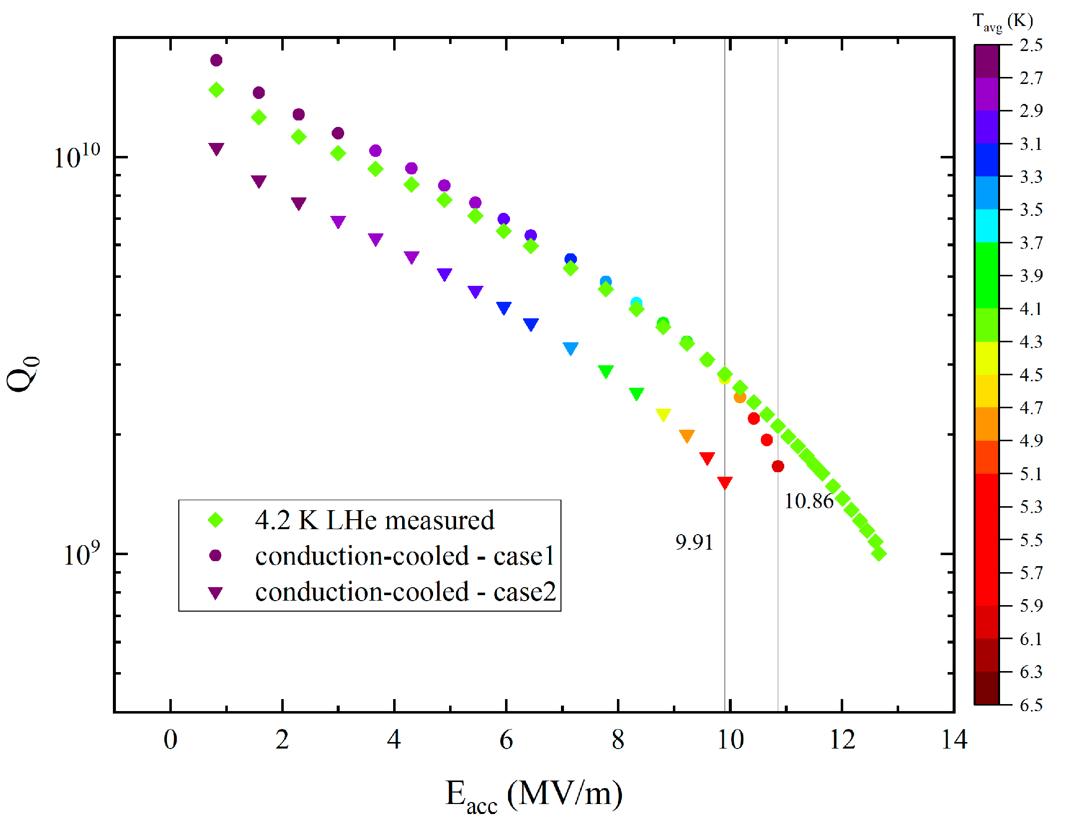
4.4. Simulation of RF Performance of NS03 Cavity

To examine the conduction-cooling RF performance of NS03 cavity when the film was not damaged or contaminated, electromagnetic–thermal simulations were performed using the following boundary conditions: (a) P l as a function of H τ , R r e s , and T s (Nb3Sn film temperature), as shown in Equation (5) [33]; (b) the temperature-dependent load curve of SRDK-418D cryocooler provided by the manufacturer; and (c) 0.1 W heat leakage from RF cables and the base.
P l = 1 2 × R s | H τ | 2 d S = 1 2 × ( 9.4 × 10 5 f 2 T e 2.2 T c T + R r e s ) × | H τ | 2 d S
There are a few assumptions made in the simulation: R B C S is calculated using Equation (3) and does not change with E a c c ; the R r e s at different E a c c is from the test in 4.2 K LHe; the contact thermal resistance ( R c ) between Al and Al and Al and Cu is 2 × 10⁻⁴ (K·m2)/W and does not change with temperature. Since R r e s comes from a limited number of gradient points, the goal of our simulations is to examine whether the conduction-cooled NS03 cavity can be stabilized at these gradient points. We calculated two cases, where the R r e s under conduction cooling is exactly the same as the test in LHe and the R r e s doubles due to insufficiently controlled cooldown or other causes. The Q 0 E a c c curves obtained for both cases are shown in Figure 18.
Figure 19 contains the results of the simulation, showing that the maximum E a c c will be at least 10.86 MV/m and 9.91 MV/m in case 1 and case 2, and a larger E a c c will not be able to converge the solution, i.e., the cavity will not be able to operate at the next gradient point. At low E a c c , P l is very small, and the T a v g is lower than 4.2 K. Therefore, in case 1, the Q 0 will be higher than that in LHe. With the increase in E a c c and the rise in T a v g , Q 0 will decrease gradually, and when the T a v g is more than 6 K, the increase in P l will be significantly faster than that of the increase in the cooling capacity, which leads to a sharp decrease in the Q 0 . In the simulation results of case 1 and case 2, the T a v g is higher than that measured at the same P l . This may be because the thermal conductivity of the Cu used in the simulation was measured on sample pieces that were sprayed without N 2 cooling and with a lower purity of 99.9% Cu powder used. The actual Cu shell on the NS03 cavity has a lower oxygen content and higher thermal conductivity than the sample pieces. Figure 19 gives the temperature distribution of the cavity operating at the 9.91 MV/m in case 2, with a P l of 8.1 W, T a v g of 5.7 K, and a maximum temperature difference of 0.18 K over the cavity. Since the Cu shell enhances the thermal stability of the cavity, and we have achieved the same temperature gradient as in LHe cooling with the synergistic control of the four heaters, we believe that this treatment on NS03 allows the Nb3Sn cavity to operate at 10 MV/m.

5. Conclusions

We have successfully designed and constructed an LHe-free cryostat with a remarkably low heat leakage of 0.02 W at 4 K, which can be used for RF testing of superconducting cavities. We performed RF tests on two Nb3Sn cavities, achieving stable CW operation and verifying the feasibility of a superconducting cavity operating under conduction cooling.
We propose a novel treatment of a cold-sprayed Cu layer and flanges on the outer surface of the cavity, which can significantly improve the thermal stability and uniformity of the cavity. Although the Cu shell obtained in this way has a lower thermal conductivity, it can be prepared quickly and has a time advantage over electroplated Cu. By reasonably arranging four heaters and controlling the power, a slow cooling near 18 K was realized, and the temperature gradient on the cavity was lower than 0.2 K/m, which significantly improved the RF performance of the cavity.
The simulation results show that the cavity sprayed with Cu treatment and the thermal links of 5N Al can satisfy the E a c c of 10 MV/m under conduction cooling. Due to our lack of experience, the cavity was contaminated and damaged to some extent during handling and processing, which is the main reason for the lower RF performance than that tested in LHe, and these can be avoided in the subsequent experiments.

Author Contributions

Conceptualization, M.R., L.L., J.H., K.Z., X.Y. and S.H.; methodology, M.R., L.L., J.H., G.W., Z.W. and D.W.; software, M.R., G.W. and H.S.; validation, M.R., L.L. and J.H.; formal analysis, M.R. and J.H.; investigation, M.R.; resources, S.Q., F.W., L.F., F.J., F.Z., K.Z., X.Y. and S.H.; data curation, M.R.; writing—original draft preparation, M.R.; writing—review and editing, M.R., J.H. and L.L.; visualization, M.R.; supervision, J.H., L.L. and S.H.; project administration, S.H., X.Y. and K.Z.; funding acquisition, S.H., X.Y. and K.Z. All authors have read and agreed to the published version of the manuscript.

Funding

This research was funded by the State Key Laboratory of Nuclear Physics and Technology, Peking University, grant number: NPT2023ZX04.

Institutional Review Board Statement

Not applicable.

Informed Consent Statement

Not applicable.

Data Availability Statement

The data presented in this study are available on request from the corresponding author.

Acknowledgments

The authors would like to thank Ningxia Orient Superconductor Technology Co., Ltd. (OSTEC) for the cavity fabrication and postprocessing. We would like to thank Plasma Giken Co., Ltd. for their technical support in cold spraying. The support from the Guangdong Institute of Laser Plasma Accelerator Technology, China, is also greatly appreciated.

Conflicts of Interest

The authors declare no conflicts of interest.

References

  1. Workshop on Energy and Environmental Applications of Accelerators. 2015. Available online: https://www.osti.gov/biblio/1358082 (accessed on 20 July 2024).
  2. Henning, W.; Shank, C. Accelerators for America’s Future. 2010. Available online: https://science.osti.gov/-/media/hep/pdf/files/pdfs/Accel_for_Americas_Future_final_report.pdf (accessed on 20 July 2024).
  3. Chmielewski, A.G. Electron Accelerators for Environmental Protection. Rev. Accel. Sci. Technol. 2011, 4, 147–159. [Google Scholar] [CrossRef]
  4. Schoenlein, R.; Elsaesser, T.; Holldack, K.; Huang, Z.; Kapteyn, H.; Murnane, M.; Woerner, M. Recent Advances in Ultrafast X-Ray Sources. Philos. Trans. R. Soc. A 2019, 377, 20180384. [Google Scholar] [CrossRef] [PubMed]
  5. Dohmae, T.; Umemori, K.; Yamanaka, M.; Watanabe, Y.; Inoue, H. Investigation of In-House Superconducting Radio-Frequency 9-Cell Cavity Made of Large Grain Niobium at KEK. Nucl. Instrum. Methods Phys. Res. A 2017, 875, 1–9. [Google Scholar] [CrossRef]
  6. Reschke, D.; Gubarev, V.; Schaffran, J.; Steder, L.; Walker, N.; Wenskat, M.; Monaco, L. Performance in the Vertical Test of the 832 Nine-Cell 1.3 GHz Cavities for the European X-Ray Free Electron Laser. Phys. Rev. Accel. Beams 2017, 20, 042004. [Google Scholar] [CrossRef]
  7. Gonnella, D.; Aderhold, S.; Burrill, A.; Daly, E.; Davis, K.; Grassellino, A.; Grimm, C.; Khabiboulline, T.; Marhauser, F.; Melnychuk, O.; et al. Industrialization of the Nitrogen-Doping Preparation for SRF Cavities for LCLS-II. Nucl. Instrum. Methods Phys. Res. A 2018, 883, 143–150. [Google Scholar] [CrossRef]
  8. McGee, K.; Kim, S.; Elliott, K.; Ganshyn, A.; Hartung, W.; Metzgar, E.; Ostroumov, P.; Popielarski, L.; Popielarski, J.; Taylor, A.; et al. Medium-Velocity Superconducting Cavity for High Accelerating Gradient Continuous-Wave Hadron Linear Accelerators. Phys. Rev. Accel. Beams 2021, 24, 112003. [Google Scholar] [CrossRef]
  9. Belomestnykh, S. Superconducting Radio-Frequency Systems for High-β Particle Accelerators. Rev. Accel. Sci. Technol. 2012, 5, 147–184. [Google Scholar] [CrossRef]
  10. Kelly, M. Superconducting Radio-Frequency Cavities for Low-Beta Particle Accelerators. Rev. Accel. Sci. Technol. 2012, 5, 185–203. [Google Scholar] [CrossRef]
  11. Pudasaini, U.; Ciovati, G.; Eremeev, G.; Kelley, M.; Parajuli, I.; Reece, C. Recent Results from Nb3Sn-Coated Single-Cell Cavities Combined with Sample Studies at Jefferson Lab. In Proceedings of the 10th International Particle Accelerator Conference (IPAC2019), Melbourne, Australia, 19–24 May 2019; JACOW Publishing: Geneva, Switzerland, 2019; pp. 3066–3069. [Google Scholar]
  12. Hillenbrand, B. The Preparation of Superconducting Nb3Sn Surfaces for RF Applications. 1980. Available online: https://accelconf.web.cern.ch/srf80/papers/srf80-3.pdf (accessed on 20 July 2024).
  13. Work on Nb3Sn Cavities at Wuppertal. In Proceedings of the Third Workshop on RF Superconductivity, Argonne, IL, USA, 14–18 September 1987; JACoW Publishing: Geneva, Switzerland, 1987; pp. 503–532.
  14. Mueller, G.; Kneisel, P.; Mansen, D.; Piel, H.; Pouryamout, J.; Roeth, R.W. Nb3Sn Layers on High-Purity Nb Cavities with Very High Quality Factors and Accelerating Gradients. In Proceedings of the 5th European Particle Accelerator Conference (EPAC*96), Sitges, Spain, 10–14 June 1996; JACoW Publishing: Geneva, Switzerland, 1996; pp. 2085–2087. [Google Scholar]
  15. Posen, S.; Liepe, M. Advances in Development of Nb3Sn Superconducting Radio-Frequency Cavities. Phys. Rev. Spec. Top.-Accel. Beams 2014, 17, 112001. [Google Scholar] [CrossRef]
  16. Posen, S.; Liepe, M.; University, C. Nb3Sn-Present Status and Potential as an Alternative SRF Material. In Proceedings of the 27th Linear Accelerator Conference, LINAC2014, Geneva, Switzerland, 31 August–5 September 2014; JACOW Publishing: Geneva, Switzerland, 2014; pp. 431–436. [Google Scholar]
  17. Porter, R.; Arias, T.; Cueva, P.; Hall, D.; Liepe, M.; Maniscalco, J.; Muller, D.; Sitaraman, N. Next Generation Nb3Sn SRF Cavities for Linear Accelerators. In Proceedings of the 29th Linear Accelerator Conference (LINAC’18), Beijing, China, 16–21 September 2018; JACOW Publishing: Geneva, Switzerland, 2019; pp. 462–465. [Google Scholar]
  18. Posen, S.; Lee, J.; Seidman, D.N.; Romanenko, A.; Tennis, B.; Melnychuk, O.S.; Sergatskov, D.A. Advances in Nb 3 Sn Superconducting Radiofrequency Cavities towards First Practical Accelerator Applications. Supercond. Sci. Technol. 2021, 34, 025007. [Google Scholar] [CrossRef]
  19. Yang, Z.; Huang, S.; He, Y.; Lu, X.; Guo, H.; Li, C.; Niu, X.; Xiong, P.; Song, Y.; Wu, A.; et al. Low-Temperature Baking Effect of the Radio-Frequency Nb 3 Sn Thin Film Superconducting Cavity. Chin. Phys. Lett. 2021, 38, 092901. [Google Scholar] [CrossRef]
  20. Jiang, G.; Wu, S.; Yang, Z.; He, Y.; Ye, Y.; Guo, H.; Li, C.; Xiong, P.; Li, L.; Huang, S.; et al. Understanding and Optimization of the Coating Process of the Radio-Frequency Nb3Sn Thin Film Superconducting Cavities Using Tin Vapor Diffusion Method. Appl. Surf. Sci. 2024, 643, 158708. [Google Scholar] [CrossRef]
  21. Dong, C.; Lin, Z.; Sha, P.; Liu, B.; Ye, L.; He, X. Preliminary Research of Niobium Cavity Coating with Nb3Sn Film at IHEP. Phys. C Supercond. Its Appl. 2022, 600, 1354107. [Google Scholar] [CrossRef]
  22. Chen, Q.; Zong, Y.; Wang, Z.; Xing, S.; Wu, J.; Dong, P.; Zhao, M.; Wu, X.; Rong, J.; Chen, J. First Results of Nb3Sn Coated Cavity by Vapor Diffusion Method at SARI. Coatings 2024, 14, 581. [Google Scholar] [CrossRef]
  23. Wang, G.; Quan, S.; Lin, L.; Ren, M.; Hao, J.; Wang, F.; Jiao, F.; Zhu, F.; Huang, S.; Yan, X.; et al. Nb3Sn Cavities Coated by Tin Vapor Diffusion Method at Peking University. Appl. Sci. 2023, 13, 8618. [Google Scholar] [CrossRef]
  24. Takahashi, K.; Ito, H.; Kako, E.; Konomi, T.; Okada, T.; Sakai, H.; Umemori, K. First Nb3Sn Coating and Cavity Performance Result at KEK. In Proceedings of the 20th International Conference on RF Superconductivity (SRF’21), East Lansing, MI, USA, 28 June–2 July 2021; JACOW Publishing: Geneva, Switzerland, 2022; pp. 27–31. [Google Scholar]
  25. Dhuley, R.C.; Posen, S.; Geelhoed, M.I.; Prokofiev, O.; Thangaraj, J.C.T. First Demonstration of a Cryocooler Conduction Cooled Superconducting Radiofrequency Cavity Operating at Practical Cw Accelerating Gradients. Supercond. Sci. Technol. 2020, 33, 06LT01. [Google Scholar] [CrossRef]
  26. Ciovati, G.; Anderson, J.; Balachandran, S.; Cheng, G.; Coriton, B.; Daly, E.; Dhakal, P.; Gurevich, A.; Hannon, F.; Harding, K.; et al. Development of a Prototype Superconducting Radio-Frequency Cavity for Conduction-Cooled Accelerators. Phys. Rev. Accel. Beams 2023, 26, 044701. [Google Scholar] [CrossRef]
  27. Ciovati, G.; Cheng, G.; Pudasaini, U.; Rimmer, R.A. Multi-Metallic Conduction Cooled Superconducting Radio-Frequency Cavity with High Thermal Stability. Supercond. Sci. Technol. 2020, 33, 07LT01. [Google Scholar] [CrossRef]
  28. Stilin, N.A.; Holic, A.; Liepe, M.; Porter, R.D.; Sears, J.; Sun, Z. RF and Thermal Studies on Conduction Cooled Nb3Sn SRF Cavity. Eng. Res. Express 2023, 5, 025078. [Google Scholar] [CrossRef]
  29. Dhuley, R.C.; Gonin, I.; Kazakov, S.; Khabiboulline, T.; Sukhanov, A.; Yakovlev, V.; Saini, A.; Solyak, N.; Sauers, A.; Thangaraj, J.C.T.; et al. Design of a 10 MeV, 1000 kW Average Power Electron-Beam Accelerator for Wastewater Treatment Applications. Phys. Rev. Accel. Beams 2022, 25, 041601. [Google Scholar] [CrossRef]
  30. Ciovati, G.; Anderson, J.; Coriton, B.; Guo, J.; Hannon, F.; Holland, L.; LeSher, M.; Marhauser, F.; Rathke, J.; Rimmer, R.; et al. Design of a Cw, Low-Energy, High-Power Superconducting Linac for Environmental Applications. Phys. Rev. Accel. Beams 2018, 21, 091601. [Google Scholar] [CrossRef]
  31. Stilin, N.; Conklin, H.; Gruber, T.; Holic, A.; Liepe, M.; O’Connell, T.; Quigley, P.; Sears, J.; Shemelin, V.; Turco, J. Conduction-Cooled SRF Cavities: Opportunities and Challenges. In Proceedings of the 21th International Conference on RF Superconductivity (SRF’23), Grand Rapids, MI, USA, 25–30 June 2023; JACOW Publishing: Geneva, Switzerland, 2023; pp. 973–977. [Google Scholar]
  32. Kubiczek, K.; Durandetto, P.; Capra, P.P.; Francese, C.; Lanzillotti, M.; Roncaglione, L.; Kampik, M.; Sosso, A. Direct Calibration of a True-Rms Ac Voltmeter against a He-Free Pulsed Josephson Standard. Measurement 2024, 236, 114981. [Google Scholar] [CrossRef]
  33. Padamsee, H.; Knobloch, J.; Hays, T.; Wilson, P.B. RF Superconductivity for Accelerators; Wiley: Hoboken, NJ, USA, 1998; Volume 52, ISBN 0-471-15432-6. [Google Scholar]
  34. Woodcraft, A.L. Recommended Values for the Thermal Conductivity of Aluminium of Different Purities in the Cryogenic to Room Temperature Range, and a Comparison with Copper. Cryogenics 2005, 45, 626–636. [Google Scholar] [CrossRef]
  35. Didschuns, I.; Woodcraft, A.L.; Bintley, D.; Hargrave, P.C. Thermal Conductance Measurements of Bolted Copper to Copper Joints at Sub-Kelvin Temperatures. Cryogenics 2004, 44, 293–299. [Google Scholar] [CrossRef]
  36. Dhuley, R.C.; Ruschman, M.; Link, J.T.; Eyre, J. Thermal Conductance Characterization of a Pressed Copper Rope Strap between 0.13 K and 10 K. Cryogenics 2017, 86, 17–21. [Google Scholar] [CrossRef]
  37. Hall, D.L. New Insights into the Limitations on the Efficiency and Achievable Gradients in Nb3Sn SRF Cavities. Ph.D. Thesis, Cornell University, Ithaca, NY, USA, 2017. [Google Scholar]
  38. Miyazaki, A.; Delsolaro, W.V. Two Different Origins of the Q-Slope Problem in Superconducting Niobium Film Cavities for a Heavy Ion Accelerator at CERN. Phys. Rev. Accel. Beams 2019, 22, 073101. [Google Scholar] [CrossRef]
Figure 1. Cryostat model drawing and installation process.
Applsci 14 06350 g001
Figure 2. Temperature distribution at steady state for two thermal shields obtained by simulation: (a) outer shield and (b) inner shield.
Applsci 14 06350 g002
Figure 3. Magnetic field distribution on the center axis of the cryostat obtained by simulation; the horizontal axis is the distance from the top of the inner magnetic shield, and the superconducting cavity is located at a distance of about 100 to 520 mm from the top.
Applsci 14 06350 g003
Figure 4. Q 0 E a c c curves of the two Nb3Sn cavities tested in 4.2 K LHe.
Applsci 14 06350 g004
Figure 5. (a) the NS04 cavity is placed on a G-10 base, and the ellipsoid is clamped to the beam tube with Cu hoops. (b) OFC hoops, straps and cavity actually installed.
Applsci 14 06350 g005
Figure 6. (a) Pictures taken during the deposition and machining processes: sealed cavity, (b) sprayed base layer, (c) sprayed 3.2 mm Cu layer and 3 flanges, (d) machining process.
Applsci 14 06350 g006
Figure 7. (a) Al plates and rings for thermal links, (b) indium foils were inserted in positions of the thermal links on the cavity, (c) cavity with thermal links installed, and (d) cavity placed in the cryostat for testing.
Applsci 14 06350 g007
Figure 8. Approximate mounting location of the thermometers ( T 1 T 11 ), magnetometers ( M a g 1 M a g 3 ), and heaters ( H 1 H 4 ).
Applsci 14 06350 g008
Figure 9. (a) Metallographic samples of niobium–copper bonding interface; (b) stress–displacement relationship with stroke between Nb and Cu during stretching process.
Applsci 14 06350 g009
Figure 10. Surface morphology of sprayed Cu on Nb samples with significant deformation of Cu particles.
Applsci 14 06350 g010
Figure 11. (a) Cu sample and PPMS sample stands, (b) installation for thermal conductivity measuring of Al plates, (c) resistance measurements and electrical conductivity calculations for Cu sample, (d) thermal conductivity of Cu samples and 5N Al plates used in experiments.
Applsci 14 06350 g011
Figure 12. The Q 0 E a c c curves of the Nb3Sn cavity for RF testing under different conditions. The color of the data points shows the T a v g of the cavity.
Applsci 14 06350 g012
Figure 13. Cavity surface temperature and ambient magnetic field variations under three cooling conditions: (a) direct cooling without controlling the cooling rate, (b) two cycles of cooling by switching the cryocoolers on and off between 30 K and 12 K, and (c) using the heaters to control the cooling rate. The location of the thermometer and heater is shown in Figure 8.
Applsci 14 06350 g013
Figure 14. Q 0 E a c c curves under the three cooling conditions. The color of the points indicates the average temperature of the cavity, and each point was at steady state during the measurement.
Applsci 14 06350 g014
Figure 15. Variations in cavity temperatures with P l for CW tests. The dashed line indicates the cavity temperature versus P l for the 1.3 GHz TESLA single cell cavity at R r e s of 25 nΩ, and E a c c of 10 MV/m. At a cavity temperature of 4.2 K, Q 0 is about 1 × 10¹⁰.
Applsci 14 06350 g015
Figure 16. R r e s E a c c curves of RF tests on NS03 cavity.
Applsci 14 06350 g016
Figure 17. Contamination or defect in the vicinity of the cavity iris: before cold spraying (a), after alcohol sonication and HPR (b).
Applsci 14 06350 g017
Figure 18. Q0Eacc curves of Nb3Sn cavity obtained by vertical testing in 4.2 K LHe and simulations of different conditions. The diamonds are test results in 4.2 K LHe. The circles are case 1: Rres is identical to that measured in LHe. The triangles are case 2: Rres is twice that measured in LHe. The color of the points indicates the average body temperature of the cavity.
Applsci 14 06350 g018
Figure 19. Temperature distribution obtained by simulation at 9.91 MV/m in case 2, (a) cavity and thermal links; (b) temperature distribution on the cavity only.
Applsci 14 06350 g019
Table 1. Heat leakage (W) in each temperature zone of the cryostat obtained by simulation.
PathwayPosition50 K10 K4 K
RadiationVacuum vessel—outer thermal shield42.4-
Outer thermal shield—inner thermal shield 0.393
Inner thermal shield—SRF cavity 0.001
ConductionG10 or titanium rods0.30.240.003
RF cables0.60.170.013
Thermometer leads0.10.0060.001
Total 43.40.8090.018
Table 2. Deposition parameters for two Nb3Sn cavities.
CavityTin Weights/gTin Chloride Weights/gNucleation Temperature/°CNucleation Time/minCoating Temperature/°CCoating Time/minAnnealing Temperature/°CAnnealing Time/min
NS040.6 + 0.8 + 1.03500270115080110060
NS030.2 + 0.5 + 0.835003001200180110060
Table 3. Cooling rate, cavity temperature gradient, and ambient magnetic field near 18 K under three cooling conditions.
CooldownCooling Rate/
K/min
Temperature Gradient/K/m B x /mG B y /mG B z /mG
12.558.724.046.71−2.47
212.390.869.79−1.60−1.35
30.060.1710.15−1.08−0.81
Disclaimer/Publisher’s Note: The statements, opinions and data contained in all publications are solely those of the individual author(s) and contributor(s) and not of MDPI and/or the editor(s). MDPI and/or the editor(s) disclaim responsibility for any injury to people or property resulting from any ideas, methods, instructions or products referred to in the content.

