1. Introduction
The development of electric vehicle (EV) battery charging has seen significant progress since the introduction of EVs in the late 19th century. Initially, early EVs faced challenges like a limited driving range and slow charging. However, advancements in battery technology and charging infrastructure have transformed EVs into a practical transportation option for many. Early EVs used lead-acid batteries, which had low energy density and needed frequent charging. In the mid-20th century, nickel-cadmium (NiCd) batteries became common, offering better energy density and a driving range of about 60 miles per charge, though they charged slowly and did not last long. In the 1990s, nickel-metal-hydride (NiMH) batteries took over as the main EV battery technology. They had higher energy density, allowing for a range of up to 100 miles per charge, and could charge faster with a longer lifespan. Today, lithium-ion (Li-ion) batteries are the most widely used in EVs. They have even higher energy density, providing a range of up to 300 miles per charge, along with fast charging and durability. As battery technology has improved, so has the charging infrastructure. Initially scarce, charging stations are now plentiful worldwide, with many supporting various EV models. Additionally, there are different charging options available to suit different needs, including Level 1 for overnight charging and Level 3 for quick charging during long trips [
1,
2].
Regarding On-Board Charger (OBC) topologies, the most used is the two-stage topology composed of an AC-DC converter stage to guarantee PFC, followed by a DC-link capacitance and a DC-DC converter stage that offers galvanic isolation and manages the battery charging process. Usually, the AC-DC stage is a step-up topology that boosts the DC-link voltage at a fixed value higher than the peak value of the grid voltage, i.e., above 340 V in 230 V AC. The DC-DC stage is usually implemented using series LLC resonant or Phase-Shifting Full Bridge (PSFB) converters that are responsible for charging the battery for the whole battery voltage range, i.e., 200–450 V for a 400 V battery [
1,
2,
3,
4,
5,
6,
7]. However, in the series LLC resonant converter, a wide voltage range of the battery pack implies that the converter operates frequently away from the resonant frequency, which results in the resonant current waveform being far from the ideal sinusoidal waveform and a decrease in the efficiency of the LLC. Also, the efficiency of PSFB topologies decreases when the system operates far away from the nominal input-output voltage gain because of the loss of ZVS operation [
8,
9]. To avoid that, in [
9], the authors present a variable DC-link scheme that guarantees no variation of the nominal operating point despite battery voltage variation. The efficiency is higher, but it is limited by the available DC-link voltage range because of the use of a boost totem-pole AC-DC topology.
Buck-boost converter topologies arise as candidates to improve whole OBC efficiency because of their capacity to establish a DC-link voltage value higher or lower than the peak value of the voltage grid. However, two-switch buck-boost topologies such as Cuk or SEPIC are eliminated because they present high voltage stress and, therefore, have low efficiency at the OBC voltage levels [
10,
11,
12]. Four-switch topologies, consisting of a combination of boost and buck converters, offer low device stress and high efficiency when they operate as a buck or as a boost, making them a good candidate to implement a variable DC-link with an AC-DC PFC stage.
In [
13], the paper explores an advanced control scheme for a non-inverting buck-boost converter used in PFC applications. It emphasizes the reduction in current stress on the converter components, which significantly enhances overall efficiency. The buck-boost converter operates through a dual switch control mechanism, intricately balancing between the buck stage and the boost stage. The buck stage meticulously manages the input current, ensuring unity power factor (PF) operation, while the boost stage is tailored to minimize the current stress, reducing the wear and potential failure of the converter components. However, despite the advanced control scheme, it presents a discontinuous input voltage that is difficult for the design of the input filter. Another drawback is related to the expected efficiency that must not be so high due to the system always operating in the buck-boost mode, which implies that all the switches are always commutating.
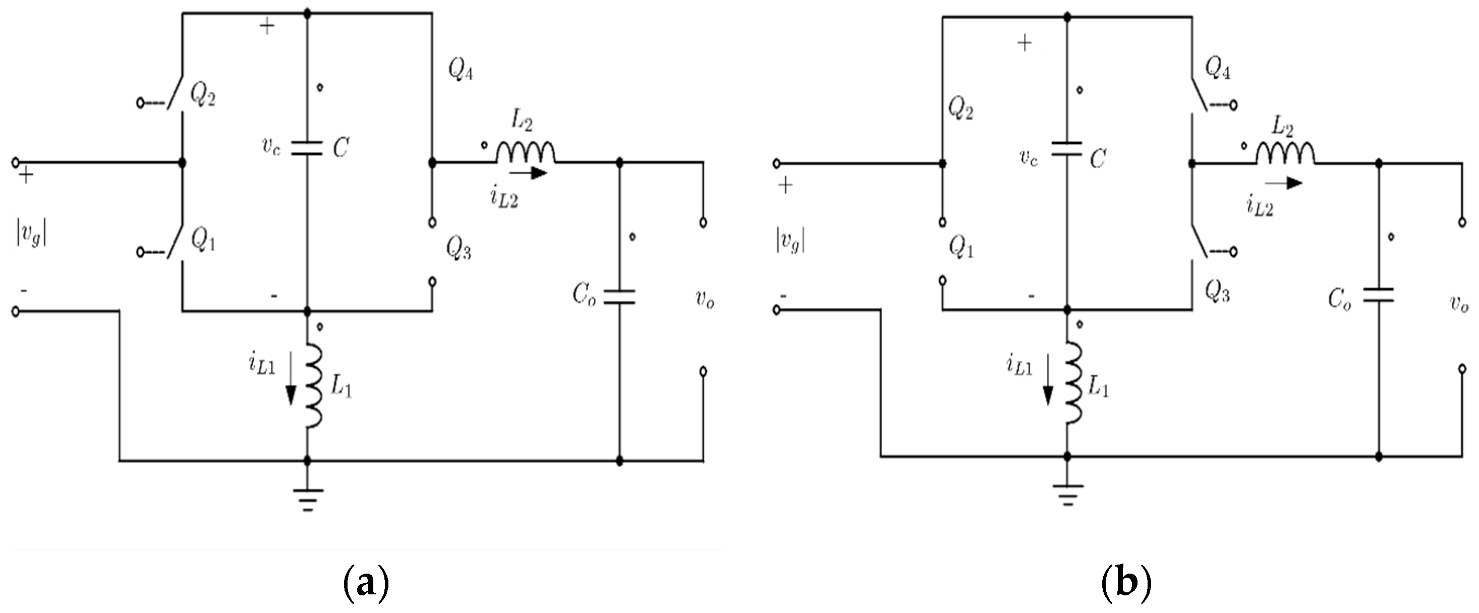
Other four-switch buck-boost converter candidates are the two-inductor topologies shown in
Figure 1, which implicitly include an input filter that ensures continuous input current. These kinds of converters present a fourth-order frequency response with two resonance peaks at frequencies lower than the switching frequency that can provoke internal oscillations.
The converter shown in
Figure 1a is presented as a novel PFC stage for EV battery charging in [
14]. The simulation results demonstrate a high PF of 0.99. Moreover, the converter can provide a wide range of output voltages. It emphasizes the converter’s potential in enhancing the efficiency of on-board battery chargers in EVs. The ability to maintain high power quality at the input while adapting to various battery voltages makes it a promising solution for the evolving EV industry. The paper concludes that this converter is an effective and adaptable solution for EV battery charging, offering high efficiency and versatility in meeting diverse charging requirements.
In [
15], there are a deeper analysis and control of the converter presented in [
14] and they are shown in
Figure 1a. The paper outlines the critical issue of Right-Half-Plane Zero (RHPZ) in the duty cycle to input current transfer function in the boost mode and the duty cycle to output voltage in both operating modes. This RHPZ presents limitations in closed-loop operation, leading to slower dynamics and suboptimal performance parameters. To overcome these limitations, the researchers explored various modifications in the converter’s design and parameters. An important development in this research is the incorporation of an RC-damping network. This network successfully addresses the RHPZ limitation, enabling a broader closed-loop bandwidth operation. A distinctive control strategy was devised and applied for both operational modes of the converter, demonstrating rapid transient response, minimal harmonic distortion, and high PF. The theoretical predictions made in the study were validated through simulated results using PSIM software. These results demonstrate the applicability and effectiveness of the proposed solutions in improving the performance of AC/DC converters for PFC applications.
This paper presents a deep dynamics and control analysis of the two-inductor four-switch buck-boost converter topology shown in
Figure 1b and its application as an AC/DC PFC stage of an OBC of an electric vehicle. This converter was previously addressed in [
16] without a detailed analysis for its instability. In this paper, the internal dynamics instability problem, due to high-Q oscillations, is solved using an RC-damping network rather than reducing the closed-loop system bandwidth, which represents the main contribution of this paper. This is a cost-effective solution, which allows the implementation of simpler controllers, avoiding the use of complicated control laws such as the one presented in [
13]. The proposed strategy enhances the PF and reliability of the converter. The simulation results validate the feasibility and effectiveness of the proposed analysis and control strategy.
In
Section 2, this paper introduces the different operation modes of the two-inductor four-switch boost-buck AC/DC converter of
Figure 1b, providing a comprehensive understanding of its circuitry. In the following section, state-space averaging and small-signal modeling are used in both boost and buck modes to realize a detailed analysis of the converter. Numerical analysis and simulation results confirming the internal dynamics instability are, respectively, delivered in
Section 4 and
Section 5. In
Section 6, the addition of an RC-damping network is analyzed. The corresponding numerical analysis is shown in
Section 7. In
Section 8 and
Section 9, this paper presents the control design and the corresponding simulations’ results, to finally summarize the conclusions of this paper in the last section.
2. Circuit Operation
This section will provide a detailed operation discussion on the AC/DC boost-buck PFC converter illustrated in
Figure 2. The analyzed converter has been specifically designed to function in CCM, where the ripple current is significantly smaller than the average current. It is important to note that the analysis of the converter assumes ideal components, including capacitors, inductors, diodes, and MOSFETs. No equivalent series resistance (ESR) or other parasitic effects are taken into consideration.
The sinusoidal input voltage is obtained from a passive 4 diodes’ rectifier, which is connected to the grid input voltage, which leads to a rectified sine wave. Two modes of operation for this converter where the power can transfer from the input to the output port occur according to the needed input and output voltages.
The first is the boost mode where output voltage is higher than input voltage. The switch
and switch
are the two primary switches for this mode.
Figure 3a can illustrate the simplified model for the boost switching model. During this mode, the switch
remains on while switch
remains off throughout the entire period. In the boost mode, inductor
and
serve as the energy transfer component. The converter operates in CCM, and has two states. Switch
is turned off while switch
is turned on in the first state. Simultaneously, charging for inductors
and
is starting and the intermediate capacitor C discharges. In the second state, switch
is turned on while switch
is turned off, allowing inductor
and
to discharge their energy and charge the intermediate capacitor C and the output capacitor
, respectively.
The second mode is buck where output voltage is lower than input voltage. The switch
and switch
are the two primary switches for this mode.
Figure 3b can illustrate the simplified model for the buck switching model. Conversely, switch
remains off while switch
remains on throughout the entire period. For this mode, the primary energy transfer component is inductor
. As the converter operates in CCM, the first state happens when switch
is turned off and switch
is turned on. The intermediate capacitor C discharges to the output load and inductor
charges. The second state occurs when switch
is turned on and switch
is turned off. At that moment, the intermediate capacitor
charges up and inductor
begins to discharge.
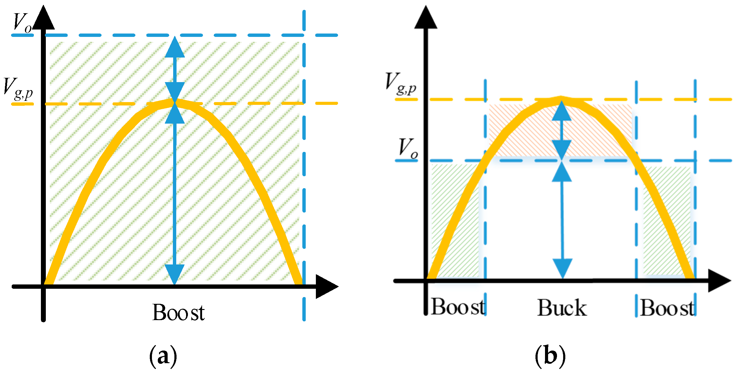
Due to the variable AC line input voltage, the converter operates in two distinct modes based on the output voltage requirements.
Figure 4 shows the operation principle for the converters, wherein the converter operates in the boost mode when
>
for the whole double line period. However, the converter operates in the buck mode, when
<
, for a portion of the double line. The rest of the period is working in the boost mode. Consequently, the converter utilizes approximately 75% of its operation in the boost mode and the remaining 25% operates in the buck mode.
3. Converter Analysis
To analyze the dynamics of the converter and develop small-signal models, state-space equations are derived for each mode of operation in this section. By analyzing the converter in both boost and buck modes separately, a comprehensive understanding of its behavior in different operating conditions can be obtained. This analysis will facilitate the design, control, and optimization of the converter for various applications.
3.1. State-Space Averaging and Small-Signal Model Analysis in Boost Mode
As mentioned, the converter operates in CCM, and the switching cycle of the converter consists of two states. The duty cycle represents the fraction of time during which the switch is on and is representing the time of the switch is off.
The state variables of the converter in the boost mode are the output capacitor voltage
, intermediate capacitor voltage
, inductor current
, and second inductor current
as depicted in
Figure 3a. Under small-ripple approximation, assuming
is positive and follows a rectified sine waveform, an analysis of the different converter switching states yields average state-space equations that describe the operation in the boost mode. These equations capture the relationships between the state variables, input voltage, output voltage, and control parameters, which can be expressed as
where
is the output resistance calculated from the output power
and average output voltage
.
Equations in (1) are inherently nonlinear due to the presence of multiplication between time-varying variables. Therefore, the linearization of the equations is necessary to facilitate the analysis. The steady-state values of the converter variables are obtained by equating the differential equations to zero. Additionally, it is assumed that the variations in
occur at a much slower rate compared to the converter dynamics, and the converter bandwidth is at least ten times lower than the switching frequency. Consequently, the converter operates in proximity to an equilibrium point, allowing it to be represented linearly. The converter dynamics around the equilibrium point can be represented as
where variables
express the dc equilibrium point or the steady-state values and the other terms
represent small variation around the steady-state values.
The obtained equilibrium points (steady-state values) are the following:
In this converter, the control objectives involve regulating the average voltage output and reshaping the line current through control of the input current . To achieve these control objectives, two transfer functions need to be calculated: , which represents the relationship between the duty cycle and the rectified input current , and , which represents the relationship between the duty cycle and the output voltage .
By calculating the transfer functions and , the converter’s control system can be designed and analyzed using classical control techniques.
These two transfer functions are expressed as follows:
where
- -
represents the small-signal variation in the rectified input current.
- -
represents the small-signal variation in the output voltage.
- -
represents the small-signal variation in the duty cycle.
3.2. State-Space Averaging and Small-Signal Model Analysis in Buck Mode
Like the boost mode in CCM, the duty cycle
is representing the time of the controlled switch
being on and
is representing the time of the controlled switch
being off.
Figure 3b presents a simplified model of the converter operating in the buck mode. Similar to the modeling procedure for the boost mode, the same approach will be followed to establish the needed transfer functions in the buck mode.
The average state-space model for the buck mode can be expressed as follows:
The steady-state values of the converter variables in the buck mode can be obtained by setting the different differential equations in (5) as equal to zero. The steady-state representation of the variables is as follows:
These steady-state values indicate the equilibrium points of the system in the buck mode, where the converter operates under stable and balanced conditions.
Similar to the boost mode, two transfer functions are expressed as follows:
where
represents the small-signal variation in the duty cycle.
4. Numerical Analysis
Table 1 represents the converter parameters that will be used for the numerical analysis. For the boost mode, the output voltage is 400 V, and 300 V for the buck mode. In circuit design, reactive elements such as inductors and capacitors were carefully selected to achieve specific ripple criteria. For boost mode operation, inductance
can be calculated from
where
is the inductor and
is the current ripple.
is the maximum input voltage.
However, for the buck mode, the second inductor
can be calculated from
where
is the second inductor and
is the current ripple.
The output capacitor
can be calculated from the following [
17]:
where
is the output power,
is the line angular frequency, and
is the peak-to-peak output voltage ripple.
Under small-ripple assumption, the intermediate capacitor voltage ripple must be similar to the output voltage ripple. With this ripple choice, the discontinuous capacitor voltage mode is avoided.
Figure 5a,b display the Bode plots for the transfer function
and
in the boost mode. The pole-zero mappings of these transfer functions are shown in
Figure 5c and
Figure 5d, respectively. It is observed that transfer function
is the minimum phase and has no RHPZ but the
transfer function has RHPZ.
Furthermore, these transfer functions exhibit high resonance undamped peaks occurring between 1 kHz and 3 kHz. These two resonance peaks below switching frequency appear in fourth-order two-inductor converter topologies under small-ripple assumption. These high resonance peaks can lead to system instability by causing oscillations and amplifying harmonic signals at their central frequencies. Managing the non-minimum phase system can be challenging, but one approach is to decrease the bandwidth and push the cut-off frequency away from the resonance undamped frequency to improve stability.
Figure 6a,b depict the Bode plots for the transfer functions
and
in the buck mode. The pole-zero mappings of these transfer functions are shown in
Figure 6c and
Figure 6d, respectively. Similar to the boost mode case, the Bode plots of the buck mode transfer functions also exhibit a high undamped resonance frequency around 3 kHz. Moreover, in this case, both transfer function
and
demonstrate a minimum phase characteristic.
The analysis of these transfer functions and their corresponding Bode plots provides insights into the frequency response characteristics of the converter in both the boost and buck modes. Therefore, to see the effects of these high undamped behaviors in the duty cycle to input current and duty cycle to output voltage transfer functions and the non-minimum phase characteristic of , simulation for the time response behavior of the converter is conducted in the next section.
5. Simulation Results
After the small-signal model analysis of the converter in the previous section, the controller can be designed to achieve the desired converter performance. In
Figure 7, a showcase steady-state waveform in different operating modes is presented wherein
Figure 7a illustrates the boost mode, while
Figure 7b displays the buck-boost mode. Each plot includes the input voltage
, input current
, output voltage
, and output current
at full load. In both modes, the regulation of the output voltage is achieved, demonstrating the converter’s ability to maintain stability and the desired output voltage level. For both modes, the PFs are more than 0.98, with 4.7% THD for the buck mode, and 3.4% THD for the boost mode.
In addition to the observed stable operation and satisfactory performance of the converter, it is important to note that there may still be underlying internal problems that require further investigation. Despite the min-phase characteristic of the transfer function relating the duty cycle to the input current transfer function, the system exhibits internal dynamics instability. This instability arises as an oscillation in the intermediate voltage in both the boost and buck modes. The Bode plots for both modes illustrate the presence of a resonance frequency range between 1 kHz and 3 kHz. This resonance frequency is also evident in the time domain waveform, manifesting as internal dynamic oscillation. The internal dynamics instability can have significant implications for the converter’s overall performance and stability. It can lead to issues such as output voltage fluctuations, reduced efficiency, and potential system damage. Managing and mitigating this instability is crucial to ensure the reliable and robust operation of the converter.
Simulation results further support the presence of high-Q oscillations caused by an internal poorly damped resonance.
Figure 8 illustrates the intermediate capacitor
waveform in the boost mode, while
Figure 9 depicts the waveform in the buck mode. Each figure includes two subplots: (a) showcasing the intermediate capacitor
waveform, which reveals the high-Q oscillations behavior, and (b) displaying the normalized Fast Fourier Transform (FFT) of the intermediate voltage
, highlighting the resonance frequency that aligns with the Bode plot, where the high-Q oscillations’ behavior occurs. These simulation results provide visual evidence of the internal poorly damped resonance with the observations made in the frequency domain analysis.
The presence of high-Q oscillations, as evident from the waveform and FFT analysis, emphasizes the importance of addressing these oscillations to ensure the stable and efficient operation of the converter. Efforts to address internal dynamic oscillation can involve various control techniques. One approach is to reduce the bandwidth by adjusting the control parameters to push the resonance frequency away from the closed-loop system bandwidth. This helps to dampen the oscillations and improve stability. Additionally, active control strategies, such as feedback control or adaptive control algorithms, can be implemented to actively regulate the intermediate voltage and suppress the internal dynamics oscillations. Another approach, which will be applied and analyzed in this work, is the introduction of a passive snubber RC circuit to damp this resonance.
6. Boost-Buck Converter Using Snubber RC Circuit
To mitigate the internal instability caused by high-Q oscillation peaks, a solution is proposed in the form of an RC snubber circuit. This section focuses on the introduction of the RC snubber circuit to dampen the resonance peak.
Figure 10 presents the modified converter configuration with the addition of a damping RC circuit (
,
) connected in parallel to the intermediate capacitor C. The RC snubber circuit is strategically placed to provide effective damping of the resonance oscillations. Other options are reducing the gain and the bandwidth of the controller. The proposed method is a simple and cost-effective solution to mitigate the high-Q oscillation peaks.
The subsequent analysis will involve the small-signal modeling of the converter in both buck and boost modes. This modeling approach enables the evaluation of stability and operational regions. By incorporating the RC snubber circuit into the system, it is expected that the damping effect will suppress the high-Q oscillation peaks, leading to improved stability and overall system performance. Through the investigation of the small-signal models and stability analysis, the effectiveness of the RC snubber circuit in enhancing the stability of the converter will be assessed.
6.1. State-Space Averaging and Small-Signal Model Analysis in Boost Mode with RC
This section will discuss the state-space average equations for the converter shown in
Figure 10 for the boost mode with the RC-damping circuit, which can be derived and expressed as follows:
The DC equilibrium equations can be expressed as follows:
The two transfer functions, the duty cycle to rectified input current and the duty cycle to output voltage , are obtained after linearization around the equilibrium point and will be used for the numerical analysis in the next section.
6.2. State-Space Averaging and Small-Signal Model Analysis in Buck Mode with RC
Similar to the boost mode, the buck mode with damping RC state-space average equations can be expressed as
The DC equilibrium equations can be expressed as
Finally, the two transfer functions, the duty cycle to rectified input current and the duty cycle to output voltage , are obtained and will be used for the numerical analysis in the next section.
7. Numerical Analysis
After obtaining the expressions for
and
in both modes of operation with the inclusion of the damping RC circuit, their Bode plots and pole-zero mappings will be analyzed. The parameters from
Table 1 are used, along with the parameters of the damping RC circuit (i.e.,
and
. Those values are obtained by generating a script code using MATLAB to find the combination values between
and
, which dampens the system high-Q oscillation peak using the system transfer functions
and
.
Figure 11a,b depict the Bode plots for the boost mode transfer functions
and
. The corresponding pole-zero mappings are shown in
Figure 11c and
Figure 11d, respectively. In
Figure 11a, due to the damping effect of the RC circuit, the high-Q oscillation peak is effectively damped. Additionally, the Bode plot of the voltage transfer function
shown in
Figure 11b presents a minimum phase characteristic.
Similarly,
Figure 12a,b display the Bode plots for the buck mode transfer functions
and
. The corresponding pole-zero plots are shown in
Figure 12c and
Figure 12d, respectively. The analysis of the Bode plots and pole-zero mappings confirms that the addition of the damping RC circuit successfully eliminates the resonance that provokes
oscillations and the RHPZ in the
transfer function in the boost mode.
8. Control Design
In the design of the small-signal model for the converter, the closed-loop small-signal block diagram is illustrated in
Figure 13. This section focuses on the design of the current controller
and the voltage controller
to achieve the desired control objectives. As shown, the converter consists of two loops: the inner current loop and the outer voltage loop. Therefore, the design process begins with the inner current loop by designing
It worth noting that
is the voltage sensor gain for the output voltage, which equals to
.
To ensure a consistently high PF by reshaping the input current waveform in all operational modes, it is essential for the inner current loop to possess a wide bandwidth, facilitating fast responses. Additionally, its crossover frequency must be kept below the switching frequency . In terms of robustness, the phase margin of the inner current loop should be greater than 45° to guarantee stability.
The inner current loop gain is a good approximation below the switching frequency and around the input voltage. This loop gain varies with the input voltage and must have sufficient stability margins for that variation.
In the boost mode, the current control transfer function
is a proportional and integral (PI) controller with a first-order low-pass filter, which has a cut-off frequency (
) at the switching frequency. The equation can be expressed as follows
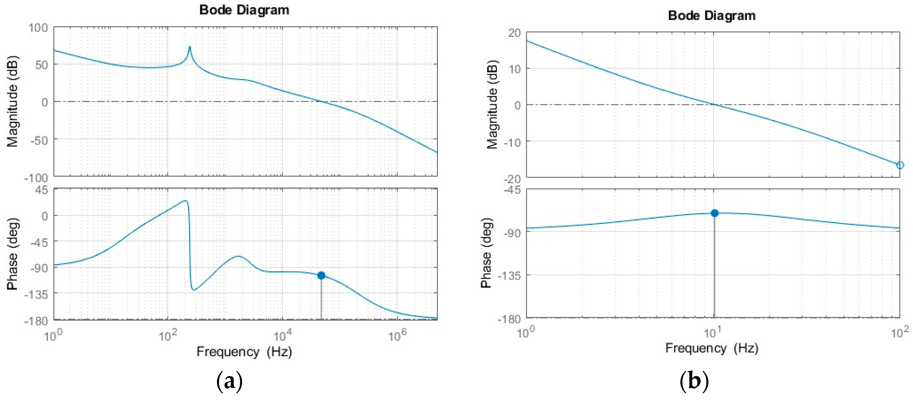
Figure 14a illustrates the current loop gain transfer function, showing a crossover frequency occurring near 110 kHz, accompanied by a phase margin of 64°.
The inner current loop can be closed and its transfer function for the closed-loop transfer function
will be
The external voltage loop, which is slower to respond, is sensitive to fluctuations in the input voltage that occur at twice the line frequency, often referred to as the double line frequency. The loop’s performance as a voltage regulator is accurately approximated only at frequencies lower than this double line frequency. Consequently, to ensure stability and adequate response, the crossover frequency for this loop must be set below the double line frequency and should be paired with a phase margin exceeding 45 degrees. The design of the output voltage controller, denoted as
, is formulated by employing the current reference to output voltage transfer function
, which is derived using
. This approach facilitates the management of the output voltage in the face of input variations and preserves system stability across the operating range. The voltage transfer function
can be expressed as follows
The voltage control loop’s transfer function, designated as
, is tailored to achieve a phase margin of 87° at a crossover frequency of 4 Hz, as depicted in
Figure 14b. This specification ensures that the system maintains stability and a timely response to changes in load or input voltage. The phase margin value of 87° provides a buffer above the minimum acceptable margin of 45°, contributing to the robustness of the control loop against variations in system parameters or external disturbances.
The selection of a 4 Hz crossover frequency, well below the double line frequency, allows the control loop to effectively mitigate the influence of an input voltage ripple and ensures a stable output voltage, which is essential for the reliable operation of power electronic systems. The transfer function for voltage control
is structured as a first-order system with an integrator and a zero at a low frequency, which can be expressed as
To streamline control operations, the same
and
transfer functions are utilized for both the buck and boost modes. This simplification contrasts with the approach taken in the referenced work [
14,
16], where distinct controller loops are implemented for each mode, leading to increased complexity and computational demand in the digital control system.
Figure 15a,b illustrate the Bode plots for the loop gain of the current and voltage transfer functions in the buck mode.
Figure 15a shows a bandwidth of 46 kHz and an almost 75° phase margin.
Figure 15b presents the Bode plot for the voltage loop gain, revealing a bandwidth of 10 Hz and a phase margin of 109°. These plots demonstrate the stability characteristics of the control system in the buck mode.
Figure 16 illustrates the schematic of a block controller used for managing a power conversion system with a dual-loop structure: one for current control and another for voltage control. The diagram indicates the process flow, starting with the sensing of the absolute input voltage
, output voltage
, and rectified input current
. These sensed values are fed into the control system for processing.
Initially, the peak of the input voltage is determined using a peak detector circuit. The sensed input voltage is then divided by this peak value to produce a normalized rectified sine waveform, termed as the voltage reference . This normalization is crucial for creating a reference that follows the input voltage’s shape but maintains a consistent magnitude, which is necessary for subsequent control actions.
The sensed output voltage is then compared with a predetermined fixed reference voltage. The objective here is to regulate the average output voltage to this fixed reference, and this is accomplished through the voltage control compensator . The compensator adjusts the system to correct any deviations from the desired output voltage.
Subsequently, the output from is multiplied by the normalized rectified sine waveform voltage reference . This multiplication yields the reference current that the current controller compensator will use to shape the rectified input current accordingly. By comparing the actual rectified input current with this reference current, the system ensures that the input current waveform is sculpted to closely match the voltage waveform, thereby achieving a high PF and efficient energy usage.
The control signals for the gates of the switching devices are generated through a dual-comparison mechanism involving a Sawtooth waveform with a 1 V amplitude. The top comparator utilizes the output from and the Sawtooth waveform to create control signals for the buck switches, which operate at the system’s switching frequency. In contrast, the bottom comparator drives the boost switches by first subtracting 1 V from the output voltage and then comparing this modified signal with the same Sawtooth waveform. This methodical generation of gate signals ensures that the buck and boost switches are driven correctly to regulate the power flow in the converter.
9. Simulation Results
To thoroughly assess the effectiveness and practicality of the suggested power conversion approach, simulation tests were executed using the PSIM software platform. These tests are pivotal for verifying theoretical design choices and for predicting system behavior under various conditions. The simulation setup integrates the power stage as delineated in
Figure 10 with the control circuitry detailed in
Figure 16, following the specifications listed in
Table 1. To enhance the realism of the simulation, equivalent series resistances (ESRs) are assigned to the inductors and capacitors to reflect actual component losses, and the switching elements are modeled to encompass their non-ideal behaviors. Additionally, parasitic effects are factored into the diode models.
Figure 17 showcases the boost mode’s steady-state behavior by illustrating the waveforms of the intermediate voltage
alongside its Fast Fourier Transform (FFT) analysis. The FFT is instrumental in identifying the spectral components of the voltage waveform, providing insights into the harmonic content and the effectiveness of the snubber circuit in mitigating high-frequency oscillations.
Similarly,
Figure 18 presents the steady-state waveforms and FFT analysis for the buck mode. When operating at full load and with the RC snubber circuit in place, both
Figure 17 and
Figure 18 offer a comparison to previous states depicted in
Figure 8 and
Figure 9. The inclusion of the snubber circuit is particularly noteworthy as it addresses the intermediate voltage
internal dynamic stability issues, a critical aspect for the reliable operation of power converters.
One of the key observations from the simulation is the absence of internal dynamic instability concerns in both operational modes, which is an essential criterion for a successful design. Furthermore, the FFT distribution for demonstrates uniformity, indicating that the snubber circuit effectively suppresses undesirable harmonic frequencies, thereby validating the design’s efficacy. This uniformity in the frequency spectrum signifies that the voltage across the intermediate stage does not exhibit excessive harmonic distortion, which could otherwise impact the performance of the power stage and the load it drives.
These simulations confirm that the proposed design operates as intended, with the power stage and control circuit working harmoniously to manage the load dynamically without introducing instability or significant harmonic distortion. The results serve as a proxy for real-world performance, offering confidence in the proposed solution’s viability for practical applications.
Figure 19 presents the boost mode steady-state waveforms of the output voltage
, output current
, input voltage
, and input current
at full load. The peak input voltage is 300 V and the output voltage is 400 V while the output current equals 8 A at full load. The input current and voltage waveforms highlight how the input current waveform precisely follows the referenced current and persists in the phase with the input voltage. This harmony makes a low distortion factor with 3.7% THD and 0.99 PF.
Figure 20 shows buck mode steady-state waveforms of output voltage
, output current
, input voltage
, and input current
at full load. The peak input voltage is 300 and the output voltage is 200 V, while the output current is 8 A. The waveforms illustrate how the input current waveform is in phase with the input voltage, exhibiting low distortion. The PF is measured to be 0.99 with 4.3% THD, indicating efficient power utilization.
It should be noted that simulation findings indicate that the resistor
dissipates approximately 3.2 W, which constitutes about 0.2% of the total power in the buck converter mode. This power loss is calculated from the buck mode, which exhibits the highest voltage ripple due to the low output voltage, as shown in
Figure 18. The power loss is determined by multiplying the voltage across the resistor
by the current flowing through it.
For boost mode operation, the design is aimed for a maximum current ripple of 12% and a voltage output ripple of 8%. These criteria were chosen based on considerations of circuit stability and performance. However, this design choice results in the buck mode exhibiting a voltage ripple of 12% due to the lower output voltage, while the current ripple is at 3%. This trade-off ensures optimal performance across different operating modes of the circuit. The output voltage ripple can be controlled by adjusting the value of the output capacitance to meet the application requirements. In this simulation, the output capacitor is set to 800 μF; for a lower voltage ripple, a higher output capacitor could be used.
These simulation results provide valuable insights into the performance of the converter with the implemented RC snubber circuit. The waveforms demonstrate the ability of the converter to regulate the output voltage, maintain high PF operation, avoid internal dynamic problems, and control the output voltage ripple within acceptable limits. The simulation outcomes support the effectiveness of the proposed solution in achieving the stable and efficient operation of the converter under various load conditions.
10. Conclusions
This study contributes to the advancement of AC/DC converter design for PFC applications, providing valuable insights into the analysis, control, and optimization of converter systems. The findings pave the way for improved converter performance, ultimately enhancing the efficiency and reliability of power conversion in various applications. The comprehensive evaluation of a power conversion approach using PSIM software simulations yields encouraging results, affirming the design’s effectiveness and practicality. The simulations, integral for corroborating theoretical decisions and forecasting system behavior under diverse scenarios, utilized realistic parameters for enhanced accuracy. This included incorporating equivalent series resistances (ESRs) in inductors and capacitors, modeling switching elements with Level 2 characteristics to account for non-ideal behaviors and considering parasitic effects in diodes. Such meticulous modeling ensures a closer reflection of real-world conditions.
A significant outcome of the simulation is the effective harmonic suppression observed in both boost and buck modes. The Fast Fourier Transform (FFT) analysis of the intermediate voltage demonstrates the snubber circuit’s proficiency in mitigating high-Q oscillations and reducing unwanted harmonic frequencies. This is crucial as it implies minimal harmonic distortion in the voltage, a key factor for the efficient performance of the power stage and the load. Stability and efficiency are other highlights of the simulated design. The absence of internal dynamic stability issues in both operational modes, coupled with high PFs (0.99 in boost and buck mode), underscores the design’s capability to dynamically manage the load without inducing instability or significant harmonic distortion. Additionally, the converter’s ability to maintain stable and regulated output voltage under full load conditions, with a controlled output voltage ripple, is a critical aspect for reliable power converter operation.
However, the introduction of a snubber circuit, while beneficial in eliminating the high-Q oscillations, brings additional losses, especially across the resistor . This necessitates an optimization trade-off to ensure minimal efficiency loss while maintaining desired performance and stability. In conclusion, these simulation results provide the vital confirmation of the proposed design’s functionality, indicating that the power stage and control circuit work in harmony. They affirm the converter’s ability to handle various load conditions effectively, maintaining stability, efficiency, and a controlled output voltage ripple, thus offering a reliable and practical solution for real-world applications.


