1. Introduction
Terahertz (THz) waves, which lie between microwaves and infrared waves with frequencies ranging from 0.1 to 10 THz, hold significant application value in fields such as medicine, security detection, and communication. Advancements in THz technology [
1] have opened up new possibilities for the creation of innovative THz devices, with THz metamaterial absorbers emerging as a particularly crucial device category. Efficiently absorbing THz waves is a key ability of THz metamaterial absorbers, playing a crucial role in utilizing THz waves for various applications. In the realm of infrared detection, the utilization of these devices can lead to the development of highly sensitive THz sensors. By manipulating the structures of materials, one can effectively achieve the shielding and concealment of THz waves in the realm of electromagnetic invisibility [
2]. When it comes to sensor technology [
3], THz metamaterial absorbers find application in the precise handling and transmission of THz waves. Hence, the progress in the realm of THz metamaterial absorbers [
4] brings about significant implications, paving the way for enhanced applications across diverse domains. Since Landy et al. [
5] proposed metamaterial absorbers based on electromagnetic resonators in 2008, research has rapidly progressed, leading to various absorber designs, including single-band [
6], multi-band [
7,
8], and wide-band [
9] absorbers. Although these absorbers have achieved some success in electromagnetic wave control, the metal–dielectric–metal sandwich structure is still used, which makes the shape and size of the absorber relatively fixed. Given the inherent rigidity of this configuration, it restricts the absorber’s ability to adapt its absorption performance dynamically to specific needs. The inflexibility of this configuration hinders the absorber from adapting its performance in real-time to cater to distinct needs, consequently restricting the effective utilization of metamaterial absorbers in situations demanding immediate performance modifications. Proposals have been made for absorbers that can be adjusted and tuned over a wideband range, utilizing materials such as graphene [
10], semiconductors [
11], liquid crystals [
12,
13], and phase-change materials [
14]. Interestingly, the utilization of VO
2 in broadband absorbers for adaptable absorption without significant frequency shifts is notable, owing to its electrical conductivity modulation techniques via thermal [
15,
16], electrical [
17,
18], or photoexcitation [
19,
20] methods. For example, Song et al. [
21] introduced a novel design, a wideband absorber utilizing VO
2, that demonstrates a remarkable capacity to modulate terahertz band absorption levels, ranging from 5% to a full 100%, yielding a significant relative bandwidth of 71% for absorption rates exceeding 90%. A configuration utilizing liquid crystal [
22] materials and employing metal disc and metal elliptical disc structures was conceptualized by researchers. In 2017, there was a notable accomplishment in achieving optimal absorption [
23] across three distinct frequency ranges. Through the manipulation of the voltage applied to the liquid crystal material, it becomes feasible to adjust the peak frequency of absorption [
24], leading to the potential for dynamic optimization of absorption capabilities. Broadband absorbers in the terahertz range are widely used in many fields. They can be used for antenna design and electromagnetic compatibility analysis in wireless communication systems, as well as in terahertz wave imaging systems and sensors, such as medical imaging, security checks, food quality testing, and other fields. Broadband absorbers in the terahertz range are also of great significance for studying the absorption and transmission characteristics of materials and can be used in the fields of materials science and optics.
Utilizing the special properties of VO
2 thin films, absorbers constructed with metamaterial capitalize on the distinct temperature phase transition characteristics of VO
2, disrupting the impedance matching conditions when triggered thermally [
25] and achieving a profound modulation effect. Displaying promising potential, absorbers containing VO
2 sub-wavelength structures exhibit remarkable capabilities in achieving high absorption modulation over a wide range of frequencies. In comparison to conventional multilayer absorbers, VO
2-based absorbers offer a simpler, ultra-thin, and dynamically adjustable solution, leading to enhanced modulation speed and reduced structural complexity [
26,
27,
28,
29]. Switching VO
2 from an insulating state to a metallic state (and vice versa) requires a temperature change of about 50 °C, which takes about tens of picoseconds and depends on various factors such as the thickness of the film and carrier density. Recent studies have shown that by combining multiple VO
2 thin films, faster switching speeds and wider absorption bands can be achieved. In addition, a higher initial laser power can be used to accelerate the switching speed. As a result, the exploration and advancement of VO
2 broadband absorbers that are broadband, ultra-slim, and can be dynamically adjusted have emerged as a central focus in ongoing research, opening up new perspectives and opportunities for improving the effectiveness of metamaterial absorbers.
This work proposes a dynamically tunable, wideband, and efficient absorber based on the phase-change material VO2. When the conductivity of VO2 reaches 200,000 S/m in its metallic phase, it exhibits excellent absorption properties, exceeding 90% absorption across a broad frequency range of 2.4 THz to 11.0 THz. Additionally, near-perfect absorption of close to 100% is achieved at resonance frequencies of 3.0 THz, 7.1 THz, 8.7 THz, and 10.6 THz. By controlling the conductivity of VO2, a transition between the functionalities of a reflector and an absorber can be freely made, enhancing its flexibility and applicability. Equally noteworthy are the features of wide-angle absorption and polarization insensitivity exhibited by the absorber, which effectively broaden its practical applications and adaptability to diverse scenarios. The findings of this study offer valuable guidance for advancing the technology of sophisticated and high-efficiency broadband tunable devices, paving the way for the continuous progress of terahertz technology and its diverse applications.
2. Structure and Research Methods
Figure 1 illustrates the structure of a terahertz tunable broadband absorber using VO
2 in its unit cell. The depicted structure reveals its three-dimensional arrangement, progressing from the uppermost layer downwards. The structure consists of two VO
2 pattern layers and a continuous gold reflection layer separated by two dielectric layers. The period of the unit cell is
p = 35 μm, the thickness of the gold reflection layer is t
1 = 0.2 μm, and the conductivity of gold is σ
Au = 4.56 × 10
7 S/m. The thickness of the VO
2 pattern layer is t
3 = 0.1 μm and the thickness of the PTFE dielectric layer is t
2 = t
4 = 7.5 μm. The dielectric constant is 2.1 and the loss angle tangent tanδ = 0.0002. The parameters of the optimized structure are: d = 2 μm, p
1 = 30 μm, r
1 = 6 μm, and r
2 = 3 μm.
The key feature of this structural unit is that it has symmetry in both the x and y directions, which is also the intrinsic reason for its polarization insensitivity. The metasurface was developed to address some of the limitations of traditional metasurfaces, such as limited bandwidth, beam shift, high loss, etc., and one of its significant differences compared to other metasurfaces that are also used for the same purpose is its higher design flexibility and modulation capability. The geometry of the metasurface has an important influence on its absorption range, and the metasurface is usually composed of microscopic scale structures. In this paper, when the designed structure is asymmetrical or the structural parameters change, the absorption range will be affected and the performance will decline, and the structure and parameters presented in this paper can achieve the best absorption performance. Therefore, in the design of a metasurface, it is necessary to consider the shape, size, periodicity, and other factors of its micro–nano structure to achieve effective control and regulation of light waves and meet the requirements of having a specific absorption range.
In the THz frequency [
30] range, the dielectric constant ε(ω) of VO
2 can be represented by the Drude [
21] model:
where
= 12 is the high-frequency relative permittivity,
is plasma frequency, σ is conductivity of VO
2, ω is the angular frequency of THz waves, γ = 5.75 ×
rad/s is collision frequency, and
can be approximated as
, where
3 ×
S/m, and
= 1.4 ×
rad/s.
The temperature has a direct impact on the conductivity of VO2, thus, the simulation calculation in this work is mainly carried out for room temperature and high temperature (350 K). The conductivity of VO2 is set to σ = 200 S/m when T = 300 K. When the temperature increases to 350 K, VO2 exhibits a metallic state and its conductivity is σ = 2 × 10⁵ S/m. In the THz frequency range, the conductivity of VO2 may also be influenced by frequency. For example, in the THz frequency range, the electron transport in VO2 films may be influenced by the frequency. When the THz wavelength matches the characteristic scale of electron migration time and charge carrier density, it can trigger oscillation and cyclotron motion of charge carriers, leading to changes in conductivity. The variation in conductivity of VO2 films in the THz frequency range may also be related to surface plasmon resonance. When the THz wavelength matches the surface plasmon resonance frequency of the film, it can induce oscillation of surface charges and thereby affect the film’s conductivity. The changes in conductivity can also impact the absorption capability of VO2 films towards THz radiation, resulting in variations in absorption bandwidth. The absorbers designed were simulated using CST Microwave Studio simulation software (2022), following an analysis of the optical properties, a study was conducted on a dynamically adaptable absorber using terahertz metamaterials. During the simulation process, the frequency domain finite element method (FEM) was used, a frequency-domain solver with tetrahedral meshing was used in simulation and the cells per max model box edge were set to 10. The distance between the port and the material surface was set to greater than 1/4 of the center wavelength, the incident terahertz waves approached the absorber from the direction opposite to the surface along the -z-axis, and the incident wave had its electric field aligned with the x-axis and the magnetic field aligned with the y-axis. The boundaries were defined by the unit cells in the x-axis and y-axis directions, and open boundary conditions were defined in the z-axis direction.
The representation of the THz absorber’s absorptance is as follows:
where R(ω) and T(ω) represent the reflectance and transmittance, respectively, and
=
=
,
represent the reflection coefficient and transmission coefficient in the S-parameters. Since the thickness of the continuous metal film in the bottom layer of the structure is much greater than the skin depth of the THz wave inside it, the incident THz wave is completely reflected. Thus,
is always 0 and Equation (2) can be directly simplified into
=
3. Results and Discussion
The results of the simulation illustrate that the conductivity of VO
2 in the metallic phase reaches a level of 2 × 10
5 S/m, enhancing the absorber’s capacity for wideband absorption. Remarkably, the absorption performance is within the range of 2.4 THz to 11 THz. We introduce
fL = 2.4 THz and
fH = 11 THz into the formula
, and we can obtain a relative bandwidth of 128.4%. The absorption levels surpass 99% at the resonance point of 3.0 THz, 7.1 THz, 8.7 THz, and 10.6 THz, achieving perfect absorption. When VO
2 is in the insulating phase, the conductivity is 200 S/m, the absorbed amount is below 2%, while the reflection surpasses 98%. By adjusting the conductivity of VO
2 from 200,000 S/m to 200 S/m, the property of VO
2 changes from a metallic state to an insulating state, and a transformation occurs in the behavior of the absorber. Illustrated in
Figure 2, it is evident that control over the absorber’s absorption and reflection is highly precise and dynamic. With the ability to manipulate both parameters within the absorption bandwidth, the ability to toggle between absorption and reflection based on specific operational needs is made possible. It is worth mentioning that, in VO
2 metamaterial absorbers, when the temperature fluctuates within the transition zone, the conductivity of the VO
2 film also changes accordingly. This change may cause a shift in the threshold frequency of the absorber, thereby altering the position and width of the absorption bandwidth. In addition, temperature fluctuations may also affect the transmission characteristics of VO
2 thin films, thereby affecting their absorption capacity at specific frequencies. As a result, the capability of VO
2 in absorption tuning lies in the manipulation of conductivity through temperature variations within the terahertz range, offering increased versatility and adaptability for practical applications, increasing the versatility and functionality of the equipment.
The theory of impedance matching is employed to clarify the physical mechanism behind achieving broadband perfect absorption. Equation (3) can be used to represent the relative impedance of the absorber:
The magnetic permeability represented by μ and the dielectric constant represented by ε appear in Equation (3). Through simulation, S11 and S21 can be derived. As a result, the S-parameter inversion method can be used to determine both the real and imaginary components of the absorber’s relative impedance.
The correlation between the capacity to absorb and the relative impedance is demonstrated by the following equation:
In Equation (4),
Z0 is the effective impedance of the surrounding environment, the impedance value is effectively controlled by the absorber, and
Zr =
Z/
Z0 is the relative impedance between the absorber and air. When the effective impedance of the absorber matches the relative impedance of air,
Zr is equal to 1; thus, achieving ideal absorption is possible for the absorber. By evaluating the absorption spectrum and the real and imaginary components of the relative impedance using
S11 and
S21 with varying phases of VO
2, as shown in
Figure 3, we can find that the real part of the relative impedance is close to 1 and the imaginary part is close to 0 when VO
2 is in the metallic phase. It is demonstrated that within the frequency range of 2.4 THz to 11 THz, successful impedance matching has been accomplished between the absorber and air, attaining remarkable absorption efficiency. Conversely, during the insulating phase of VO
2, the values of the real and imaginary parts of the relative impedance are close to zero, indicating an interruption in impedance matching between the absorber and air. Due to this transformation, the absorber shifts from its absorption function to its reflection function. This transition allows the absorber to adapt its properties between absorption and reflection modes depending on different operational conditions, thereby enhancing its versatility and adjustability.
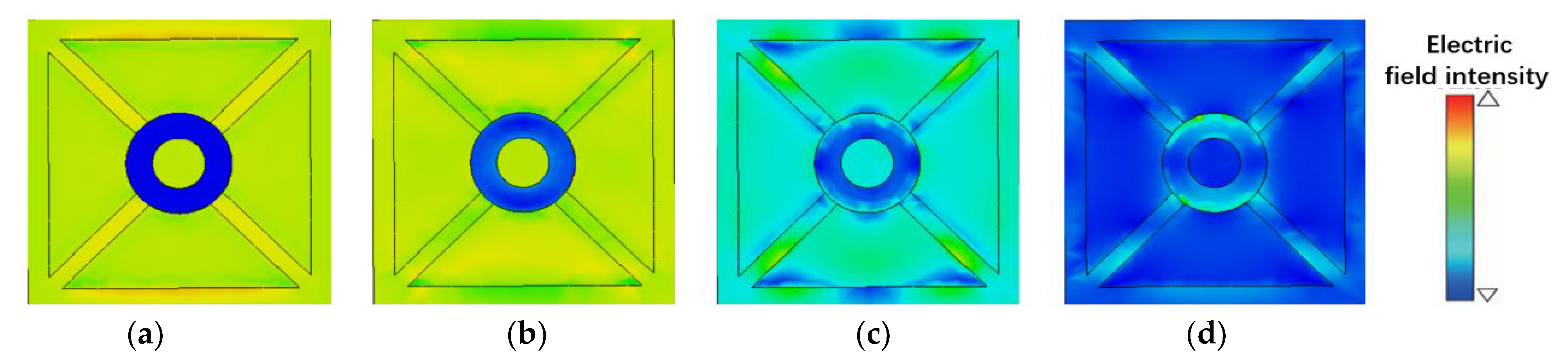
In order to further investigate the physical mechanisms of the metamaterial absorber, the electric field distribution in the z plane of the top-layer microstructure at the near-perfect absorption point of the absorber was studied when the conductivity of VO
2 is set to 200 S/m, 20,000 S/m, 80,000 S/m, and 200,000 S/m, as shown in
Figure 4. It is evident that at a conductivity of 200 S/m, VO
2 remains in an insulating phase, resulting in minimal electric field distribution on the resonant layer. This leads to terahertz waves easily penetrating through the resonant layer, resulting in a relatively minimal absorption. As the conductivity of VO
2 increases, the electric field tends to focus within the voids of the VO
2 design. Upon achieving an electrical conductivity of 200,000 S/m, there is a noticeable emergence of the electric field distribution surrounding the annulus. This leads to an increased influence of the resonating and reflecting layers on terahertz waves, resulting in a higher level of absorption. VO
2 exhibits sensitivity to variations in temperature, allowing for indirect control of its conductivity through temperature adjustments, resulting in a dynamic tuning capability for wideband absorbers. This feature is not attainable with conventional metal-based absorbers. Broadband absorbers utilizing VO
2 have the capability to switch actively between absorption and reflection, with the added feature of dynamic regulation through temperature management. This opens up new avenues for exploration in the realm of multifunctional THz devices.
In order to fully understand the influence of absorber structural parameters on its absorption characteristics, a detailed study was conducted on the absorption spectrum of the absorber structure under different parameters.
Figure 5a shows that there is a decrease in absorption observed at the 5 THz frequency for the absorber as the size r
1 increases. There is hardly any alteration observed in the absorption profile as the dimension r
2 is raised. This phenomenon is a result of the gradual reduction in the strength of the electric field at the outer perimeter of the ring when r
1 is adjusted, thereby diminishing the absorber’s reaction to incident THz waves and causing a drop in absorption. In contrast, modifications in r
2 do not impact the electric field strength at the outer edge of the ring. By examining the electric field discussed previously, it is evident that alterations in the electric field’s intensity are more pronounced at the perimeter of the circular structure. In contrast, during the insulating phase of VO
2, there is minimal distribution of the electric field within the VO
2 layer. Therefore, modifying the dimensions of the loop using either r
1 (the outer radius of the VO
2 ring) or r
2 (the inner radius of the VO
2 ring) does not exert a significant influence on the absorption rate due to the low sensitivity of the absorber configuration to THz waves. From
Figure 5, it can also be seen that when the values of r
1 or r
2 are changed, a small absorption peak appears near 9.6 THz. This may be due to the fact that when VO
2 is in an insulating state, its band structure becomes more separated, resulting in a significant enhancement of light absorption within a specific wavelength range.
Exploring the impact of varying polarization and incident angles on the absorber’s absorption capabilities holds significant importance. Absorbers exhibit insensitivity to polarization and can effectively absorb across a wide range of angles. The study delved into how the absorber performs at various polarization orientations and incident angles of incoming THz waves. By adjusting the THz wave’s polarization angle from 0° to 90°, we obtained the absorption spectrum of the absorber corresponding to various polarization angles. The absorption spectrum of the absorber under varying polarization angles is shown in
Figure 6a. This implies that the absorber is insensitive [
31] to polarization angle, a trait mainly attributed to the symmetry of its structure. This characteristic allows the absorber to remain unaffected by the polarization phase of the incident light. A separate investigation of the absorption spectrum was conducted under different polarization modes, namely TE and TM polarization. The results are shown in
Figure 6b,c. With an increase in the angle of incidence, the rate of absorption exhibits a decline. Nevertheless, across a broad range of incident angles up to 60°, the absorber demonstrated consistent absorption performance for both TE and TM waves. Over a spectrum of incident angles below 60°, the frequency range of 3–11.4 THz still exhibited a wide bandwidth for the TE polarization mode, in which the absorption exceeded 90%. In the TM polarization mode, the peak absorption of the broadband absorber could still be maintained above 90% when the incident angle was below 69°.
Compared to the work of others, the proposed THz absorber has certain advantages in terms of bandwidth, absorption rate, and angular stability, as shown in
Table 1 [
28,
32,
33,
34].


