Featured Application
This is the first time to be issued of a new clean agent can applied into wafer dicing process of silicon contaminant cleaning directly.
Abstract
A new cleaning agent for silicon contamination in the wafer dicing process was formulated in this research. Ammonium bifluoride was introduced as the main ingredient in the formula, and MSA and sulfuric acid were added as the solvent and buffer solution against metal corrosion. It was confirmed that the new formula cleaning agent could be used in the cleaning of silicon contamination from dicing. Silicon contamination is common in the wafer dicing process and consists of silicon powder and relevant metal particles during cutting, all of which are mixed with some adhesive residues. These contaminating particles on the IC surface are exposed to cleaning agents. However, while it is imperative to clean the wafer, the exposed surface is also vulnerable to damage from the solution. This further complicates the procedure because there is currently no ideal cleaning agent for the process. Our proposed formula hopefully provides an ideal chemical for use in wafer cleaning (SC-1, SC-2, BOE), since it uses a less toxic compound, ammonium bifluoride, which yielded good results during our experiments.
1. Introduction
In 1958, Bell Labs began using silicon wafers to make transistors in wafer, transforming all semiconductors into silicon-based products. As the manufacturing technologies of integrated circuits advanced, silicon transistors were applied in more sectors such as computers, mobile devices, automobiles, etc. With this transition to silicon-based semiconductors, they also developed a wafer dicing process that turned out to be a rather polluting and irreparable procedure, not to mention that production with this process was either a complete success or complete failure. Therefore, the race is on for engineers to improve the technique for better dicing quality and higher yields. Nevertheless, the process continues to be plagued by many uncontrollable factors, which are either human or machine in nature, and these do not include other, external factors such as water, power, gas, and air shortages that further contribute to the contamination and damage of the wafer surface. In addition, the lack of proper cleaning agents and procedures in the dicing industry has forced companies to discard a large number of dies (ICs), burdening them with financial costs and losses, as well as creating a negative impact on the environment.
1.1. Level of Silicon Contamination
In this study, we categorized the severity of contamination into three levels (Table 1). Level 1 includes deposits of contaminating fine powder around the bumps; given the granule size, this is by far the most difficult to remove using current technology. Level 2 comprises deposits of silicon contamination in non-bump areas, which are easy to remove using existing agents on the market. In Level 3 are the water marks left on the wafer surface; these are also easy to clean using existing cleaning agents on the market.

Table 1.
Three levels of silicon contamination.
1.2. EDX Analysis of Silicon Contamination
The contaminants from the dicing process can be analyzed by energy-dispersive X-ray spectroscopy (EDX) analysis (shown to include Si, Cu, N, and O elements), which may include not only solid elements or chips from the diamond blade but also adhesive residues from UV glue of tape or base film (Figure 1). The EDX analysis explains why it is difficult to remove these contaminants, especially those in Level 1, where fine powder of silicon is deposited around the bumps, shielding them from cleaning agents by shadow effect.
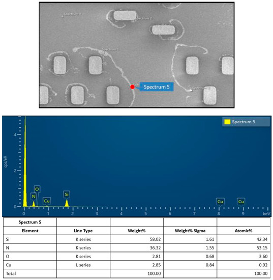
Figure 1.
EDX analysis of silicon contamination finding elements of Si, N, O, and Cu, all mixed with other residues from the dicing blade, taping, glue, etc.
1.3. History of Cleaning Agents in the Semiconductor Industry
The earliest known cleaning agent, SC-1, for semiconductors was first developed in 1970 by Kern and Buodinant of the Radio Corporation of America (RCA) [1], and the formula remains the most used agent for cleaning in the semiconductor manufacturing industry.
The formula of SC-1 is NH4OH:H2O2:H2O, mixed in the ratio of 1:1:5 to 1:2:7, and it can remove organic contaminants on wafers in an operating temperature range of 70–80 °C. Another formula, of SC-2, is HCl:H2O2:H2O, mixed in the ratio of 1:1:6 to 1:2:8, and it can remove inorganic contaminants on wafers in an operating temperature range of 70–80 °C. Given that wafers are pure silicon, the main ingredient in these cleaning agents is hydrofluoric acid (HF), which in its vapor form can remove the oxide layer on silicon wafers in the semiconductor IC process and can be combined with hydrogen peroxide (H2O2) or ammonia water (NH4OH) to enhance the cleaning. However, these formulas are not suited wafer the dicing process because the ingredients in these agents are corrosive to metals, including Al, Cu, Ni, Ti, TiW, Sn, etc., which are common elements used in the semiconductor manufacturing and packaging process (Figure 2).
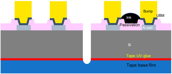
Figure 2.
Cross-sectional illustration of wafer after dicing, showing various materials exposed to the cleaning agent.
There are other cleaning methods, such as UV-ozone treatment, which was developed by Vig in 1985 [2]. Another method for cleaning the wafer involves using oxygen plasma cleaning [3]. However, despite the availability of these materials and methods to clean wafers, they are still not suited for cleaning after dicing.
2. Materials and Methods
2.1. Challenges of Cleaning the Contamination
As shown in Figure 2, the cross section of a wafer is exposed after dicing, making it susceptible to the actions of cleaning agents that target not only both the organic and inorganic contaminants (such as the passivation layer on the IC, aluminum metal (Al) trace, and a composite of copper metal (Cu), titanium (Ti), and titanium tungsten (TiW) metals), but also the residues from adhesive tapes, ink marks and other non-metal objects. Therefore, a suitable cleaning agent candidate should remove the silicon contaminants without disrupting the adhesiveness of the tape, i.e., have the properties of dissolving silicon but with non-corrosiveness to the wafer surface, which is, at best, contradictory in terms of function and makes it quite a challenge to develop a proper cleaning agent [4].
2.2. Types of Cleaning Agents for Wafer Dicing on the Market
There are many cleaning agents available on the market. Each supplier has their own specific formula and instructions, but regardless, they can be classified into four categories, as shown in Table 2. The first type is a pure solvent. The second type is an alkaline solution. The third type is an alkaline agent with surfactant. The fourth type is known as a photoresist stripper.
Table 2.
Four types of cleaning agents on the market that are applied to the dicing process.
In this study, we also tested the performance of seven types of commercial cleaning agents. It was found that both SP-700 stripper and buffered oxide etch (BOE) (HF + NH4F) effectively removed Level 1 silicon contaminants (Table 3), while the other agents failed.
Table 3.
Comparison of the performance of different cleaning agents.
Although the stripper was capable of removing Level-1 silicon contamination, it was more aggressive and corrosive, even against ink marks, tape adhesives residues, IC metals, etc. Therefore, to clean the contaminants on an IC surface, it is recommended to move the entire die away from the dicing frame to another special platform for manual cleaning. This process of relocating for decontamination and manual cleaning often delays the production process, in turn increasing financial costs or losses. BOE, on the other hand, is only aggressive and corrosive against metals. Thus, if a protective mechanism can be devised to shield the system from corrosion, BOE can be a potential agent for cleaning the wafer directly during the dicing process.
2.3. Formation of Contaminants
Silicon contaminants from dicing are similar in principle to residual water stains, as they both interfere with the function of the wafer [5,6]. The major difference involves the reactions that may occur at the interfaces between two substances. For example, reactions may take place between Si powder and water, as described in Equations (3) and (4).
Water stains are the most common type of contamination seen on a blank wafer. The formation has been described as follows in the literature [6]. When water droplets are on the wafer surface, the following two reactions will occur between the air and the water droplets, as well as between the water droplets and the wafer. First, O2 molecules in the air will dissolve into the water droplets, and together, they react with the silicon atoms on the surface of the wafer, as illustrated in Equations (1) and (2). The reactions are as follows:
2H2O + Si ⇌ SiO2 + 4H+ +4e−
Si +O2 ⇌ SiO2
The product, SiO2, will continue to react with water to produce silicic acid (H2SiO3) [6,7,8,9,10,11,12], as shown in Equations (3) and (4):
SiO2 + H2O ⇌ H2SiO 3
H2SiO3 ⇌ H+ + HSiO3−
As the water evaporates, the monomers of silicic acid in the water will gradually polymerize into dimer or trimer complexes to form insoluble polymers of polysilicic acid [6,7,8,9,10,11,12] that are deposited on the surface of the wafer. Polysilicic acid and silicon dioxide are the residual stains [13,14]. Similarly to the formation of water stains in the literature [6,15], the formation and characteristics of silicon contaminants from dicing are as detailed in Figure 3.
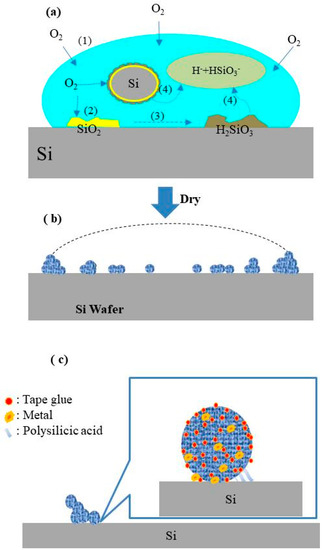
Figure 3.
The formation of silicon contamination on the wafers. (a) The chemical reaction mechanism of the formation of silicon contamination on wafer; (b) The Silicon contamination condition after water dried; (c) The assumed microstructure of silicon contamination.
Although silicon contaminants are similar to the water stains on the wafer surface, the aforementioned reaction of silicic acids will occur on both the water and contaminant surfaces, leaving residues of silicic acids on both sides. Given the presence of silicic acids on both surfaces as described by this mechanism, only an agent that dissolves silicic acid can remove the silicon contaminants (Table 3, test 4 and 7) [7,8,9,10,11].
2.4. Mechanism of Contaminant Cleaning
To summarize the results listed in Table 3, we assumed the bonding forces of silicon contamination to have include three sources, as follows:
- Silicic acid bonding
- Glue adhesive residue
- van der Waals forces
The major force comes from silicic acid bonding, since it is chemical bonding. The next force is that from the glue adhesive residue, which involves polar attraction. The last and minimal force is van der Waals force. As the results in Table 3 show, only agents that can dissolve silicic acid can remove the contamination.
The alkaline surfactant can clean Level 2 and Level 3 contaminants, but not those in Level 1. It is assumed that it can assist with Level-1 contaminant cleaning, but it is not the main agent for that purpose. Extra agitation is needed when cleaning the contamination; this agitation is believed to be effective against van der Waals forces.
Figure 4 is the assumed cleaning mechanism for silicon contamination, and it indicates which cleaning agents may be chosen. The main agent should have the ability of dissolve polysilicic acid. The next agent should be able to dissolve glue residue on contaminant particles but not attack the UV tape glue or ink marks. A dispersing agent may be used with the new cleaning agents, since preventing reprecipitation is very important and needs to be taken into consideration. Other additives such as metal protectants are key to whether a new cleaning agent can be used in the dicing process or not.
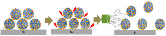
Figure 4.
There are two main steps in the process of cleaning silicon contamination: the first is to dissolve the bonds of polysilicic acid, the particle-to-particle bonds, and the bonds between the particles and the surface of the IC; in the second step, water spray or a brush is used to cause agitation between the contamination particles, thus aiding the silicon contamination removal efficiency.
2.5. Development of a New Cleaning Agent
Five targets needed to be achieved by the new cleaning agent developed in this research.
- Full cleaning of the silicon contamination (Levels 1 to 3)
- No IC trace (Al) corrosion remaining after cleaning process
- No more UBM under cut to enhance
- No gel residue
- In mark area, residue is more than 80% and is readable.
Existing agents used in the cutting process, such as the stripper and alkaline solvents, are mostly alkaline based. However, given the fact that the contaminants are primarily bound together by the interaction between water and silicic acid polymers (Figure 3), we would propose a cleaning agent based on the acidic properties of HF (BOE) [16].The chemical reactions involved are shown in Equations (5) and (6) below [17]:
SiO2 + 4HF + 2NH4F ⇌ (NH4)2SiF6 + 2H2O
SiO2 + 6HF ⇌ H2SiF6 + 2H2O
Since HF is highly toxic to the human body, we used NH4F-HF instead to verify the cleaning effect against silicon contamination [18,19,20,21].
The IC metal is mostly aluminum and must be protected during the manufacturing process. The role of sulfuric acid in the cleaning agent is to provide hydrogen ions (H+) in solution. Additionally, as noted in the literature, metal can be passivized when the sulfuric acid exceeds a specific concentration; that will be prevented from occurring during the cleaning process [5,22,23].
In addition to the silicon element, there are other contaminants such as the adhesive glue, the dicing tape, the metal chips from the blade and other materials from the IC dicing assembly line (passivation material, SiO2, Al, Cu, etc.) [24].
Therefore, in order to successfully remove these contaminants, a proper solvent, in addition to ammonium bifluoride as an ingredient, must be added [25], but must not be so strong as to erode away the exposed IC metals [22]. Methane sulfonic acid (MSA) was selected as the solvent for this research. Since it is a derivative of sulfate, it formed a buffer solution of sulfuric acid, which allowed us to control the release of hydrogen ions (H+) and adjust the acidic acid level and prolong the lifespan of the cleaning agent [5]. MSA has an R group, which is –CH3, giving it the ability to dissolve glues. The combination of the organic R group and an inorganic sulfate also gives it the properties of surfactant, further enhancing its cleaning strength [5].
For a comprehensive review, N-methylethylamine (MEA) and propylene glycol methyl ether acetate (PGMEA) were included in the testing list. Four groups of tests were planned for this research. The first was to test the performance of the alkaline (MEA) formula, the second to test the solvent-based formula (PGMEA), the third to verify the surfactant additive, and the fourth to study the acidic formulas assumed in Section 2.4 (ammonium bifluoride/sulfuric acid/MSA).
3. Results and Discussion
The combination of MEA and ammonium bifluoride rendered the cleaning agent ineffective in removing Level-1 contamination, but this preparation was good for the other concerns, such as leaving no CI trace corrosion, no UBM under cut, and no gel residue and not attacking ink marks.
The combination of propylene glycol methyl ether acetate (PGMEA) solvent and ammonium bifluoride (Figure 5) rendered the cleaning agent ineffective in removing Level-1 contamination as well as other contaminants such as glues from the dicing tape.
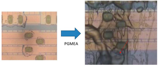
Figure 5.
PGMEA, as a solvent, not only obstructed ammonium bifluoride from cleaning Level-1 silicon contaminants (shown by the red arrow) but also dissolved the UV glue from the dicing tapes, leaving more residues on the IC surface.
As seen in Figure 6, ammonium bifluoride in acidic conditions (H2SO4 + NH4F-HF) could effectively remove Level-1 silicon contamination. This result proved the assumptions of Section 2.4.
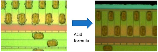
Figure 6.
Cleaning results with ammonium bifluoride in acid formula, with the right side showing clear removal of all contaminants.
In Test 3 of Table 4, the results confirmed that the combination of ammonium bifluoride in high concentration with sulfuric acid could effectively remove Level-1 contaminants (Figure 6), without corroding the aluminum metal [8,22]. Additionally, no signs of disruption of the adhesive materials from the dicing tape and ink dot were observed, but when the solution came in contact with under-bump metal (UBM), the peel-off of the bumps was noticeable (Figure 7).
Table 4.
Summary of Cleaning Performance for Si Contaminants.
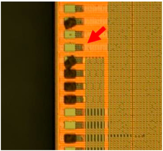
Figure 7.
Bump peeled off (at the red arrow) after 15 min of applying the cleaning agent in Test 3 of Table 4, with UBM being etched completely by such acidic formula.
The comparison of Test 3, 4, and 6 in Table 4 showed that the mixture of H2SO4 and NH4F-HF left the ultraviolet (UV) glue of the cutting tape and ink marks intact, while it only removed Level-1 silicon contamination. Higher concentrations of H2SO4 could indeed protect the aluminum metal, but not UBM (Ti/TiW) [5,26,27].
Test 5 in Table 4 found that the non-ionic surfactant additive did not remove the contaminants by a general ionic mechanism, as expected, but by the chemical reaction of micro-etching, as illustrated below in Equation (7) [5,26,28,29].
H2SiO3 + 6NH4F-HF → H2SiF6 + 3H2O + 6NH4F
The reaction product of H2SiF6 is soluble in water, so NH4F-HF could effectively remove the polysilicic acid to free the silicon powder from bonds with the wafer surface, which in turn could be easily removed [1,30]. The NH4F solution served as a chemical buffer to ammonium bifluoride, such that it slowed down and stabilized the etch efficiency [17,20].
When comparing Test 7 and Test 8 in Table 4, we found that methane sulfonic acid (MSA) could protect UBM metals, but the solution’s ability to remove contaminants was significantly reduced (possibly because without dissociation of ammonium bifluoride, silicon dioxide and polysilicic acid cannot be dissolved) [31]. Moreover, it was found that MSA did dissolve the dicing glue and ink marks, as expected (Test 7 in Table 4).
Table 4 lists a summary of the tests performed on the alkaline formula (Test 1), solvent base formula (Test 2), and formula with surfactant additive (Test 5), in this study of acidic formulas for cleaning agent.
When comparing the results of Test 3 and Test 8 in Table 4, we found that MSA could reduce the corrosion of UBM (Ti/TiW) during cleaning (Figure 8). This result means MSA may absorb on under-bump metal (Ti/TiW) surfaces during the cleaning process and prevent H+ and F− ions from penetrating and corroding the UBM. This result may be applied to the development of a UBM etchant.
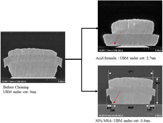
Figure 8.
Comparison of UBM under cuts after 15 min of applying cleaning agents of different formulas in acid formula and 30%MSA, revealing MSA as an inhibitor that protected UBM in acidic solution of ammonium bifluoride.
The results of Test 9 in Table 4 suggested the MSA concentration could prevent ink mark attack and lower ammonium bifluoride concentration would lead to lower under-bump metal (UBM) under cut.
4. Conclusions
The function of ammonium bifluoride is to free silicic polymers from the silicon contaminants on the IC surface by micro-etching. This will release the silicon contaminants from the wafer surface to be cleaned physically by the agent [18,25].
Sulfuric acid in the solution of the cleaning agent provides hydrogen ions (H+). As mentioned in the literature, a specific concentration of sulfuric acid will lead to the passivation of metal, such as in this case, the aluminum, which in turn prevents any corrosion of the metal during the cleaning process. Our test proved the hypothesis as well [22,23], which also implied that the formulas of cleaning agents in this study could be used to remove Si contamination, provided the cleaning time can be tightly controlled.
The corrosion-resistant properties of aluminum in the cleaning agent may be rendered ineffective by adding non-ionic surfactant. We speculated that the surfactant reduced the surface tension of the passive metal layer to create defects or micro-cracks, where acid would slip through to directly react with and corrode the pure aluminum metal.
The replacement of water with MSA could indeed stop the corrosion of the chip’s circuit metal (Al) and the under-bump metal (Ti/TiW). The possible explanation is that ammonium bifluoride cannot be dissociated in MSA and becomes shielded from corrosion, but it also loses the ability to remove silicon contaminants. However, we also found that MSA acted as an organic solvent to dissolve the UV glue on dicing tapes. In other words, MSA improves the cleaning strength of solutions used in removing organic materials, and given that Level-1 contamination does include adhesives such as the dicing tape, the presence of such an organic solvent will certainly assist in cleaning the silicon contaminants.
This study showed that MSA helped the under-bump metal (Ti/TiW) to resist corrosion by the cleaning agent, especially when the cleaning time was well-controlled, which translated to control of the UBM under cut. Based on these results, we confirmed that the proposed cleaning agent formula could be used in the cleaning of silicon contamination from dicing.
Author Contributions
Conceptualization, C.-Y.W.; methodology, C.-Y.W.; validation, C.-Y.W.; investigation, C.-Y.W.; writing—original draft preparation, C.-Y.W.; writing—review and editing, T.-H.T.; supervision, T.-H.T. All authors have read and agreed to the published version of the manuscript.
Funding
This research received no external funding.
Institutional Review Board Statement
Not applicable for studies not involving humans or animals.
Informed Consent Statement
Not applicable for studies not involving humans.
Data Availability Statement
Not applicable.
Acknowledgments
The authors are very grateful to Judy for supporting this research, and to the CHIPBOND Technology Development Team of John, Vincent, and Hsiang Chiu for machine operation and testing.
Conflicts of Interest
The authors declare no conflict of interest.
References
- Kern, W.; Puotinen, D.A. Cleaning solutions based on hydrogen peroxide for use in silicon semiconductor technology. RCA Rev. 1970, 31, 187–206. [Google Scholar]
- Vig, J.B. UV ozone cleaning of surfaces. J. Vac. Sci. Technol. A 1985, 3, 1027–1034. [Google Scholar] [CrossRef]
- Oehrlein, G.S.; Scilla, G.J.; Jeng, S.J. Efficiency of oxygen plasma cleaning of reactive ion damaged silicon surfaces. Appl. Phys Lett. 1988, 52, 907–909. [Google Scholar] [CrossRef]
- Brachmann, E.; Seifert, M.; Oswald, S.; Menzel, S.B.; Gemming, T. Evaluation of surface cleaning procedures for CTGS substrates for SAW technology with XPS. Materials 2017, 12, 1373. [Google Scholar] [CrossRef] [PubMed]
- Affrossman, S.; Daviot, J.; Holmes, D.; Pethrick, R.A.; Wilson, M. Molecular design for inhibition of titanium corrosion in resist cleaner systems. Corros. Sci. 2001, 43, 939–950. [Google Scholar] [CrossRef]
- Chen, X.; Xu, Y.; Zhang, S.; Isoya, S.; Shimao, S. Research on Surface Watermark Analysis of Wafer Cleaning Process. In Proceedings of the 2012 Conference on Society of Manufacturing Engineering—SME, Notre Dame, IN, USA, 4–8 June 2012. [Google Scholar]
- Sharafeev, S.M.; Pogrebenkov, V.M. Phase Formation Processes in Natural Magnesium Silicates of Various Structures by Ammonium Fluoride Treatment. Refract. Ind. Ceram. 2020, 61, 200–206. [Google Scholar] [CrossRef]
- Liu, X.; Liu, C.; Meng, C. Oligomerization of Silicic Acids in Neutral Aqueous Solution: A First-Principles Investigation. Int. J. Mol. Sci. 2019, 20, 3037. [Google Scholar] [CrossRef]
- Putz, M.V.; Russo, N.; Sicilia, E. On the applicability of the hsab principle through the use of improved computational schemes for chemical hardness evaluation. J. Comput. Chem. 2004, 25, 994–1003. [Google Scholar] [CrossRef] [PubMed]
- Putz, M.V. Density functionals of chemical bonding. Int. J. Mol. Sci. 2008, 9, 1050–1095. [Google Scholar] [CrossRef]
- Putz, M.V. Maximum hardness index of quantum acid-base bonding. MATCH Commun. Math. Comput. Chem. 2008, 60, 845–868. [Google Scholar]
- Putz, M.V. Chemical action concept and principle. MATCH Commun. Math. Comput. Chem. 2011, 66, 35–63. [Google Scholar]
- Mondal, B.; Ghosh, D.; Das, A.K. Thermochemistry for silicic acid formation reaction: Prediction of new reaction pathway. Chem. Phys. Lett. 2009, 478, 115–119. [Google Scholar] [CrossRef]
- Goto, K. Effect of pH on Polymerization of Silicic Acid. J. Phys. Chem. 1956, 60, 1007–1008. [Google Scholar] [CrossRef]
- Houston, M.R.; Maboudian, R.; Howe, R.T. Ammonium Fluoride Anti-Stiction Treatments for Polysilicic Microstructures. In Proceedings of the 8th international Conference on Solid-State Sensors and Actuators, and Eurosensors IX, Stockholm, Sweden, 25–29 June 1995. [Google Scholar]
- Williams, K.R.; Muller, R.S. Etching Rates for Micromachining Processing. IEEE J. Microelectromechanical Syst. 1996, 5, 256–269. [Google Scholar] [CrossRef]
- Blackwood, D.J.; Borazio, A.; Greef, R.; Peter, L.M.; Stumper, J. Electrochemical and Optical Studies of Silicon Dissolution in Ammonium Fluoride Solutions. Electrochem. Acta Print. Great Br. 1992, 37, 889–896. [Google Scholar] [CrossRef]
- Niwano, M.; Takeda, Y.; Ishibashi, Y.; Kurita, K.; Miyamoto, N. Miyamoto Morphology of hydrofluoric acid and ammonium fluoride-treated silicon surfaces studied by surface infrared spectroscopy. J. Appl. Phys. 1992, 71, 5646–5649. [Google Scholar] [CrossRef]
- Kalem, S. Synthesis of ammonium silicon fluoride crypto crystals on silicon by dry etching. Appl. Surf. Sci. 2004, 236, 336–341. [Google Scholar] [CrossRef]
- Gerischer, H.; Lübke, M. On the Etching of Silicon by Oxidants in Ammonium Fluoride Solution. J. Electrochem. Soc. 1988, 135, 2782. [Google Scholar] [CrossRef]
- Bahri, C.N.A.C.Z.; Ismail, A.F.; Majid, A.A. Synthesis of thorium tetra fluoride (ThF4) by ammonium hydrogen bifluoride (NH4HF2). Nucl. Eng. Technol. 2018, 51, 792–799. [Google Scholar] [CrossRef]
- Huang, J.J.; Lin, C.H.; Ho, Y.R.; Chang, Y.H. A study of aluminum oxide passivation films by liquid phase deposition and its application for ultraviolet solid-liquid hetero junction photodetectors. Surf. Coat. Technol. 2019, 391, 125684. [Google Scholar] [CrossRef]
- Mirhashemihaghighi, S.; Światowska, J.; Maurice, V.; Seyeux, A.; Zanna, S.; Salmi, E.; Ritala, M.; Marcus, P. Corrosion protection of aluminum by ultra-thin atomic layer deposited alumina coatings. Corros. Sci. 2016, 106, 16–24. [Google Scholar] [CrossRef]
- Chang, W.; Hsuan, T.T. Study on Anti-Degradation Methods of Silicon Cutting and Wafer Cleaning after Cutting; National Taipei University of Technology of Resource Engineering: Taipei, Taiwan, 2020. [Google Scholar]
- Peng, B.; Zheng, D.; Yu, Y. Method to remove wafer surface particles. IEEE J. Semicond. 2017, 38, 096004. [Google Scholar] [CrossRef]
- Ku, C.M.; Cheng, S. Factor Design for the Oxide Etching Process to Reduce Edge Particle Contamination in Capacitively Coupled Plasma Etching Equipment. Appl. Sci. 2022, 12, 5684. [Google Scholar] [CrossRef]
- Barkhudarov, P.M.; Shah, P.B.; Watkins, E.B.; Doshi, D.A.; Brinker, C.J.; Majewski, J. Corrosion inhibition using super hydrophobic films. Corros. Sci. 2008, 50, 897–902. [Google Scholar] [CrossRef]
- Tamura, H.; Ito, N.; Kitano, M.; Takasaki, S. A kinetic model of the dissolution of copper (II) oxide in EDTA solutions considering the coupling of metal and oxide ion transfer. Corros. Sci. 2001, 43, 1675–1691. [Google Scholar] [CrossRef]
- Said, M.; Nazeri, M.F.M.; Sharif, N.M.; Kheawhom, S.; Mohamad, A.A. Corrosion properties of Cu/Sn–3.0Ag–0.5Cu/Cu solder butt joints fabricated by conventional reflow and microwave hybrid heating. Corros. Sci. 2022, 208, 110641. [Google Scholar] [CrossRef]
- Hu, Y.; Fu, H.; Wang, J.; Sun, R.; Wu, L.; Liu, Y.; Xu, J.; Liu, J.; Peng, K.Q. Carbon induced galvanic etching of silicon in aerated HF/H2O vapor. Corros. Sci. 2019, 157, 268–273. [Google Scholar] [CrossRef]
- Hossain, S.T.; Johra, F.T.; Jung, W.G. Fabrication of Silicon Carbide from Recycled Silicon Wafer Cutting Sludge and Its Purification. Appl. Sci. 2018, 8, 1841. [Google Scholar] [CrossRef]


Disclaimer/Publisher’s Note: The statements, opinions and data contained in all publications are solely those of the individual author(s) and contributor(s) and not of MDPI and/or the editor(s). MDPI and/or the editor(s) disclaim responsibility for any injury to people or property resulting from any ideas, methods, instructions or products referred to in the content. |
© 2023 by the authors. Licensee MDPI, Basel, Switzerland. This article is an open access article distributed under the terms and conditions of the Creative Commons Attribution (CC BY) license (https://creativecommons.org/licenses/by/4.0/).