1. Introduction
Waveguide slot array antennas (WSAAs) are becoming increasingly important and necessary in many common applications. This guarantees outstanding advantages, such as high performance, low losses, high mechanical strength, high power handling, withstanding harsh temperature conditions, ruggedness, and reliability [
1,
2,
3,
4]. Additionally, with the continuous development of science and technology for practical electronic applications, it is required that the equipped antenna has the characteristics of being multi-function, multi-service, flexible, and intelligent.
In response to these factors, research and development efforts have concentrated on multi-band and multi-polarized antennas with notable improvements in system performance [
5,
6,
7]. Among them, antennas with polarization-agile ability can provide polarization information, such as abundant resolution, penetration, and reflection properties from observed targets. Therefore, in modern systems, such as radar, communication, and remote sensing at high frequencies, there is a requirement for dual-polarization with design goals for wide bandwidth, high gain, high efficiency, low sidelobe levels, and low cross-polarization [
8,
9,
10,
11,
12,
13].
In [
14,
15], dual polarization was produced on the same waveguide structure, with the input electronic signal traveling via the coupling slot and into the cavity. The complex structure with many overlapping layers included feed networks, coupling slots, electromagnetic field conversion cavities, and radiation slots. Making dual-polarized array antennas highly configurable and difficult to fabricate requires powerful fixation techniques based on sophisticated brazing and bonding facilities. For the sake of simplicity, the dual polarization of the WSAA is designed separately on two different waveguides.
Conventional rectangular waveguides have broad wall dimensions larger than 0.7
, so interlacing them on the same aperture to produce dual polarization is a significant obstacle as the distance between the radiating slot elements in the plane perpendicular to the waveguide axis are larger than 1
. This decreases the effectiveness of the dual-polarized array due to the formation of grating lobes during the scanning of the electromagnetic beam [
16]. In other words, it is difficult to produce effective radiation patterns in a dual-polarized array using conventional rectangular waveguides so that the grating lobes are not visible. An adopted structure that reduces the standard waveguide size is the ridged waveguide developed for both vertical and horizontal polarization.
In [
17], a VP array was produced from longitudinal slots engraved on the broad wall, and an HP array was produced from transverse slots on the narrow wall. The transverse slots have the advantage of producing a low degree of cross-polarization, which increases the polarization purity. However, this has the major disadvantage of having to be excited through the position and dimensions of the additional iris inside the waveguide near the transverse slots. However, integrating the auxiliary excitation elements inside the waveguide leads to a very difficult fabrication process because of the high machining accuracy requirements and the expensive manufacturing cost. The inclined slot suggested in [
18] takes the place of the transverse slot to ease fabrication challenges with a simple easy-to-design structure that achieves less than −25 dB cross-polarization in the Ka-band.
This result shows that the dual-polarized array has low polarization purity due to the characteristic influence of the inclined slot for the HP. In [
19,
20], the authors presented a V-shaped slot structure for an HP array with a good low level of cross-polarization achieved by the combination of the electromagnetic (EM) field perpendicular to both sides of the V-shape. The EM field complements the in-phase horizontal polarized components and eliminates the out-of-phase vertical polarized components. The excitation of the V-shaped slot is through the depth and inclination of the slot, without the need for additional resonant components. The combination of a V-shaped slot array for HP and a longitudinal slot array for VP achieves high polarization purity ideal for dual-polarized arrays.
However, the operating bandwidth is still limited, and this is also an inherent disadvantage for resonant waveguide slot arrays. One technique to increase the operating bandwidth is to separate an array into two consecutive subarrays on each side of the feed using a center feed. This also eliminates the beam squinting versus frequency due to the long line effects that occur with the end feed [
21]. To facilitate and ease the fabrication of waveguide slot array antennas, three-dimensional (3-D) metal-printing technology has been provided in [
22,
23,
24]. It unmistakably demonstrates great benefits, such as accurate machining, high manufacturing efficiency, low cost, and flexibility in structural design. More importantly, opting for monolithic 3-D metal printing helps avoid performance degradation and assembly errors.
In this paper, a compact 3-D metal-printed dual-polarized RWSAA is proposed with enhanced performance of wide operating bandwidth, low cross-polarization, high efficiency, and high isolation for X-band applications. In addition to the performance of the array, the configuration factor is also considered in order to provide strong stability with a simple structure, easy manufacturing, and low cost. The dimensions of the waveguides are miniaturized using ridged waveguides and are homogeneity aligned for both VP and HP. At the same time, the distance between the slot elements in the resonant array is also ensured for the horizontal plane. For VP arrays, standard longitudinal slots are employed, whereas V-shaped slots are utilized for HP arrays to create low cross-polarization.
The operating bandwidth is improved step by step in the design process by different methods implemented for both the radiated slots and the feed network. Utilizing the structure of periodic unit cells was studied for each pair of slots in VP and HP, separately, and combined with Elliott’s design equation to find the optimal resonance values for a 1 × 8-element linear array.
The central feeding networks are designed for each VP and HP linear slot array, separating an array into two subarrays to expand the operating bandwidth. A two-way power divider providing equal amplitude and a 180° phase difference is used for the two subarrays of VP. With a T-junction between the radiated waveguide and the coaxial-to-RWG transition in the lower layer, this is excited by a probe attached to the ceiling of the RWG. The HP array uses a direct feed from a coaxial-to-RWG transition that offers equal amplitude and phase to the two subarrays on either side and is excited with a probe attached to the ridge of RWG. The final optimized design of the 2 × 8-element dual-polarized array was fabricated by 3-D metal printing. Experimental measurement results are presented to confirm the validity of the design.
2. Antenna Array Configuration
The proposed geometric configuration for the dual-polarized RWSAA is shown in
Figure 1. The complete antenna structure is formed by a pair of linear RWSAAs with orthogonal polarization VP and HP arrays that operate simultaneously in the same X-band with a center frequency of 9.8 GHz. The radiation element of the two linear arrays is divided into two halves at the center of the waveguide, symmetrical in both the
x and
y directions with respect to VP but in the same direction with respect to the HP array as depicted in
Figure 1a. The VP linear array is performed by eight longitudinal slots etched on the upper broad wall of the RWG. The HP linear array is produced by the inclination of both sides of the V-shaped slot and is cut into the ridged broad wall of the RWG.
The V-shaped slot has a perpendicular electric field separated into VP and HP radiation components. The VP components are out-of-phase, so the radiation field is suppressed, while the in-phase HP components complement each other and achieve an ideal low cross-polarization level. The two linear arrays are interleaved with each other, so, in the z direction, the HP array is arranged one layer higher than the VP array to provide good polarization isolation and reduce the influence of mutual coupling between the radiation slot elements.
Figure 1b illustrates the inside structure of the RWG for each of the VP and HP linear arrays with a central feeding technique for the eight-element slot array. The VP array uses a two-way equal-split divider, which is a T-junction between the coaxial-to-RWG transition and the radiated RWG with the top of the coaxial probe attached directly to the ceiling of the RWG, whereas the HP array attaches the coaxial probe to the ridge of the radiated RWG. A pair of irises is needed near the coaxial probe to obtain good impedance matching.
From there, the detailed layer-by-layer structure of the proposed dual-polarized array is shown through the cross-section in
Figure 1c. This feeding method enhances the operating bandwidth, and the uniform mechanical grid structure of the pair of linear arrays has robust and light profiting. Furthermore, both the VP and HP are excited by two commercial SMA connectors with the coaxial probe feed from the bottom through a coaxial-to-RWG transition. The simple and compact feed structure provides good mechanical stability with low voltage to avoid electrical breakdown [
25].
The waveguide cross-sectional dimensions are denoted by , , and for the VP linear array, and , , and for the HP linear array. The waveguides are designed to be uniformly dimensioned with the same width and height to simplify the structure, reduce the hardware layer, and ease the manufacturing process. To contribute to the weight reduction of the array, adjacent waveguides share the same wall with a thickness of t. The waveguide resonant slot array is designed based on the strict requirement of spacing between radiated elements. Therefore, for dual-polarized RWSAA, the spacing between radiated slots needs to be considered simultaneously on both the VP and HP planes. This is to ensure radiation efficiency when combining dual polarized subarray models developed for a large array, and grating lobes are eliminated in the case of a scanned beam.
For the WSAAs, the radiating slots should be arranged with an element spacing of 0.5
along the
x and
y directions for uniform illumination. In our design, for simplicity, both VP and HP arrays are configured to have the same guided-wavelength
. Therefore, the slot element spacing is set as
=
= 0.5
= 0.5
= 0.5
, where
and
are the guide wavelengths in the radiating waveguide of the VP and HP array, respectively. As shown in
Figure 1d, the two ends of the radiated waveguide are terminated by two metal plates representing the short circuit, with the distance to the center of the last slot being
. Finally, the aperture size of the proposed dual-polarized RWSAA is 23.2 × 179.6 mm.
3. Antenna Design and Analysis Procedure
3.1. Compact Dual-Polarized Ridged Waveguide Array
Dual-polarized slotted waveguide array antennas have high power capability and mechanical stability. The configuration of the array must be decided to determine the unit cell dimensions and structure to be used during the design process. To ensure the array performance, the requirements for the spacing between radiating elements in the waveguide of a resonant array must be met. As a result, the dimensions of the waveguide need to be selected appropriately in the operating frequency band and must meet the compactness of the design. In
Figure 2, a comparison of three prototypes of air-filled waveguide structures is given, including a conventional rectangular waveguide together with two proposed compact RWGs for VP and HP.
In
Figure 2a, a conventional rectangular waveguide (WR-90) typically has an
A broad wall dimension of 0.75
and a
B narrow wall dimension of 0.33
at the highest frequency in the operation band. When two conventional rectangular waveguides are combined in the azimuth, they create a dual-polarized structure with a total size of approximately 1.2
, including the wall thickness. In this case, the distance between the waveguides is more than one wavelength, and the grating lobes in the azimuth plane completely overlap the visible region at any scanning angle [
17]. Therefore, it is difficult to produce effective radiation patterns in the HP using conventional rectangular waveguides so that the grating lobes are not visible.
Since the distance between the waveguides is limited to less than one wavelength, ridge loading should be used to achieve the required guided wavelength without exceeding the waveguide width limit. Two RWGs for VP and HP are proposed for dual-polarized arrays to miniaturize the waveguide dimensions and reduce the distance between elements in the array. The RWG width is limited by two factors: The first is that the effective operating bandwidth of the RWG is defined as the frequency range between the two cutoff frequencies in the fundamental propagation mode (dominant mode and second mode). The second is the distance of the adjacent linear arrays with respect to the radiation so that no grating lobes appear when the beam is scanned.
When the polarization scans along the waveguide axis, the spacing between the slot elements for the linear resonant array inside the waveguide should be half the guide wavelength, which means that = 0.5. To obtain uniformity between the beam squints in the VP and HP arrays, the guide wavelengths used in both polarizers must be the same. This forces the distance between the co-polarized waveguides to be equal when the scan polarization is perpendicular to the axis of the waveguide. Therefore, the optimal width for a pair of waveguides is = = 0.5 = 0.725 = 22.2 mm, and each RWG used for vertical and horizontal slots has a corresponding width of = = 0.327 = 10.008 mm, excluding wall thickness t = 1 mm.
The dominant and second mode determines the effective bandwidth of the waveguide prototypes TE10 and TE20, respectively. Since these modes are unaffected by changes in the waveguide height, the size of the array can be decreased by reducing the height of the RWG. The choices of height are limited by the vertically polarized elements. The height is chosen to be neither too small to produce bandwidth problems for slot excitations nor too large to restrict the range of radiative emissions from vertically polarized slots. The height of the optimal RWG is = = 0.25 = 7.66 mm.
As shown in
Figure 2b, the wave propagation constant curves represent rectangular waveguides and two RWGs. By tuning the size of the ridge to match the width of the RWG, the cutoff frequencies of the operating modes change. It can be clearly seen that, comparing RWGs and conventional rectangular waveguides in the first mode, the dispersion characteristics are almost the same but are more extended in the second mode, while the cross-section occupies only half. Thus, both RWGs and conventional rectangular waveguides achieve available bandwidth that is suitable for the design in the X-band.
3.2. V-Shaped Slot for Low Cross-Polarization
In the dual-polarized array, the VP linear array is easily achieved by cutting longitudinal slots into the broad wall surface of the RWG. In the HP linear array, the inclined slot is a potential solution to simplify the design without using additional sub-ingredients inside the waveguide to excite the resonant slot. However, excitation for slots using inclination suffers from several disadvantages. Along with the desired longitudinally polarized electric field, the inclination also creates an undesirable vertically polarized electric field. This increases the cross-polarization level of the dual-polarized array and reduces the performance of the antenna.
Figure 3 depicts the electromagnetic (EM) field distributions of the two proposed slot types for HP. It can be seen that the surface EM distribution for the inclined slots cutting into the ridged sidewall of the RWG is similar to that on the narrow wall of a conventional waveguide, and the radiated electric field of the V-shaped slot is a combination of a pair of inclined slots on the ridged side wall of the RWG. For each certain angle of inclination (
), the slots have an EM field distribution
E in two directions perpendicular to the coordinate axes
and
corresponding to VP and HP.
In
Figure 3a, with two linearly inclined slit arrays, the
components are suppressed due to being out of phase, while the
components are in phase, so they complement each other. Thus, the cross-polarization of a conventional inclined slot array can be suppressed by a pair of adjacent linear arrays with mirroring of the inclined slots. However, the distance (
) between the inclined slots in free space affects the performance of the cross-polarization suppression; with shorter
, better cross-polarization is achieved [
26]. From there, the inclined slots on the two waveguides are combined to create a V-shaped structure on a waveguide as shown in
Figure 3b.
Both sides of the V-shaped slot also have the same EM field distribution as do the separate inclined slots. The HP components are in phase, so the EM field radiation is uniformly combined, while the out-of-phase VP components are suppressed. With a shorter distance, the canceled EM radiated field obtains a better low cross-polarization and does not need to depend on the combination of adjacent linear arrays. Thus, the V-shaped slots achieve better performance than the inclined slots in eliminating the cross-polarization component.
3.3. Characterization of the Radiation Unit Cells
The dual-polarized array configuration and the arrangement of the two types of longitudinal and V-shaped slots were established for the VP and HP linear arrays, respectively. To achieve uniformity and optimization for both polarizers, a common design process was applied to each linear array. The periodic unit cell structure simulation method was used to analyze the characteristics of the radiation slot pairs, through Ansys high-frequency structure simulator (HFSS) software. This method assumes that the slot to be modeled is in an infinite array medium with identical elements and introduces an infinite array approach to characterize the slots.
For designs of planar arrays, the array can be considered infinite in both directions. Therefore, the simulation model for unit cells with the longitudinal slots for VP and the V-shaped slots for HP are shown in
Figure 4a,b, respectively. With the expectation of the exact same field distribution in the hypothetical environment of infinite arrays, periodic boundary conditions are applied to the free space boundaries facing each other. Specifically, if two facing boundaries are periodic, then one is chosen as the “Master Boundary”, and the other is selected as the “Slave Boundary”.
While the top boundary of the unit cell is designated as the radiation boundary, it is set up for multimode excitation through a Floquet port for periodic boundary conditions. This is based on the modal decomposition that the fields inside each unit cell of a large planar array possess. Simultaneously, the slots in the unit cell must be excited with equal amplitude and desired phase difference. Therefore, two TE10 dominant mode excitation wave ports are placed at each end of the RWG to obtain the required characteristic scattering parameters of the slot.
In the design of a resonant slot array antenna, in order to achieve radiation in the boresight, the slots etched in the broad wall must be spaced at a distance equal to half a guide wavelength. At the same time, adjacent slots have differences in symmetry along the transverse and longitudinal axes of the waveguide. Specifically, the longitudinal slots for the VP array differ in the offset direction, which is opposite to that of the adjacent slots.
The V-shaped slots for the HP array differ in the mirroring direction, which is inverse to that of the adjacent slots. This makes it necessary to use two slots inside a unit cell during the design process. This approach provides sufficient accuracy along with the influence between adjacent coupling slots, matching the slot parameter requirements when applied to large arrays. The boundaries of the air box surrounding the waveguide are defined as radiation boundaries except for the bottom boundary, which is defined as PEC and has a chosen dimension of 1× 1× 1.
For the slots on the RWG, an equivalent model is constructed with the slots as shunt admittances linked by sections of ideal transmission lines as illustrated in
Figure 4c. This model implies that the scattering from the slot is symmetrical with the backscattering (
B) equal to the forward scattering (
A).
A scattering analysis mechanism is required to control the radiated amplitude and phase of the slots, including the slot offset (), slot length (), slot depth (), and inclined angle (). The slot scattering matrix obtained after unit cell simulation is analyzed to derive the equivalent circuit parameter . The value y, which normalizes the characteristic admittance of the transmission line is given by the components of the two-port scattering matrix as follows: .
The slot parameters are tuned to obtain the imaginary part (
) representing zero normalized susceptance, and the real part (
g) representing the normalized conductance value of the characteristic normalized self-admittance (
y) (see
Figure 5). Once
y is determined, an efficient design process for the resonant slotted array developed by Elliott et al. is applied, which greatly reduces the computation and simulation for a large array. It considers the slots as two equivalent dipoles with mutual resistance compensation, including the single waveguide slot self-admittance, reciprocity theorem, and mutual coupling between two slots. Due to random presence, we use the first part of Elliott’s method for estimating the initial values of the slot lengths, slot deeps, and slot offsets in the linear array.
3.4. Parameter Extraction of Radiation Slots
The first parametric sweep is performed with the width of the radiation slot to find the initial optimal value for all slots in the antenna array. It is observed that the width of the slot has an effect on the bandwidth of the slot [
20], and the frequency sweeps are performed in the operating frequency region for three different slot widths of 1.5, 2.0, and 2.5 mm as shown in
Figure 5. The variation rate of self-admittance tends to increase as the slot width is larger but decreases the radiated power of the slot. When the slot is wider, the excitation distance between the elements will be larger, and the radiative effect on the slot will be smaller. This restricts the maximum power, which can be radiated by a slot in the array to a lower value. Therefore, the optimal parameter selected for the width of the slot is
= 2 mm.
For the longitudinal slots in the VP array, the iterative approach to find a valid set of initial slot parameters is as follows: an appropriate offset is chosen to perform a slot-length parameter sweep to obtain values for the normalized conductance and resonance length at the design frequency. The curves about
versus
and the obtained results for normalized resonant conductance
g are summarized in
Figure 6.
The normalized conductivity is uniform and proportional to the increase of the groove deviation and the resonance length as the mutual coupling effect between adjacent waveguides is reduced by the radiation waveguide structures of the HP array interwoven between the VP array, thereby increasing the isolation.
For the inclined slots in the HP array, through each value of inclination angle selected to sweep the resonant slot depth parameters, the resonance conductivity values are recorded. The extracted parameter curves about
versus
and the obtained results for
g are summarized in
Figure 7. It is found that the normalized admittance curves diverge with the increase of the tilted angle. Different from the VP array, the normalized conductivity of the HP array is inversely proportional to the increase in inclined angle but proportional to the increase in resonant depth. In order to excite each slot while being in phase and spaced by a half-guided wavelength, adjacent V-shaped slots are arranged symmetrically and in opposite directions.
Both the HP and VP linear arrays are designed to follow the uniform distribution array with a side lobe level (SLL) of 13.26 dB. The radiated power and resonant conductance of a slot are proportional to the square of the voltage excitation of the slot. The equivalent value of the resonant conductance is calculated as in [
17]:
where,
= 2 is the matching condition for the center feed of the linear slot array. The number of slots
N = 8, and
= 1 is the voltage excitation for each slot. Therefore, the normalized conductance of each slot is calculated as
=
. Once the slot conductance is known, the slot parameters can be determined based on the curves in
Figure 6 and
Figure 7. Thereby, the design parameters for the longitudinal slot are
= 19.15 mm and
= 1.25 mm and, for the V-shaped slot, are
= 4.0 mm and
= 23.75°.
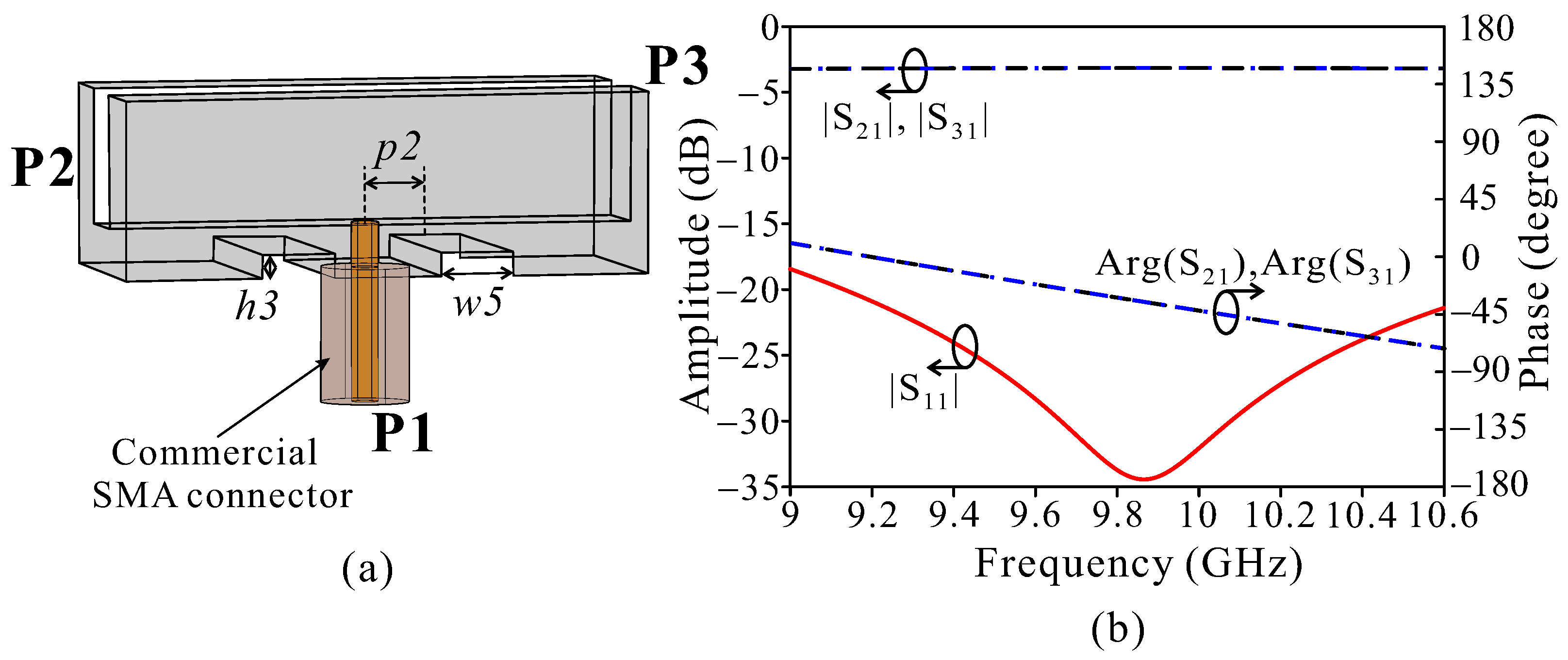
3.5. Design of Feeding Structure
For the VP array, central feeding is realized through a coaxial-to-RWG transition connected to a T-function power divider as shown in
Figure 8, where
Figure 8a is a two-way equal-split divider that offers the symmetrical left-half and right-half of the radiated waveguide and uses a tuned H-shaped coupling slot structure to ensure a signal phase difference of 180° over broadband. The discontinuous impedance induced at the junction of the power divider is matched to a metal step on the ridge of the feeding RWG.
The ridge height is properly increased in the proximity of the coupling slot to increase the equivalent capacity of the transmission line and, thus, reduce its impedance. The results of the power divider in
Figure 8b show good impedance matching
< −22 dB, and the out-of-phase simulate is 180° for the two output ports achieved over the full design frequency band of 9.4–10.2 GHz. Then, a coaxial-to-RWG transition is applied to use the SMA connector feed for the VP array as shown in
Figure 8c. The RWG is directly excited by the coaxial probe through a transition with a wideband short circuit and an impedance matcher with two irises symmetrically across the center of the coaxial probe above the ridge.
A wideband short circuit is created when the coaxial probe is attached directly to the ceiling of the RWG, reducing the reflection of incident waves to the input port. By tuning the position of the coaxial probe, combined with the appropriate size and distance of the iris pair, the bandwidth efficiency of the transition is enhanced.
Figure 8d shows the results of the transition in the design frequency band of 9.4–10.2 GHz, and matching impedance is achieved with
< −25 dB.
For the HP arrays, a feed is applied directly from the coaxial-to-RWG transition with an SMA connector as shown in
Figure 9. The coaxial probe is attached to the underside of the ridge in the radiated RWG as shown in
Figure 9a. The position of the coaxial probe is placed in the center of the radiated waveguide to ensure the equal amplitude and phase for the two sides of the subarray. The V-shaped slot radiation elements in the left-half and right-half of the waveguide are placed in the same direction.
A pair of symmetric irises on either side of the coaxial probe is added to expand the operating bandwidth of the transition.
Figure 9b shows that the feed of the HP array achieved good impedance matching
< −25 dB with equal amplitude and was in phase at the two output ports over the design frequency band of 9.4–10.2 GHz. The simple ridged waveguide slot array feed structure provided good operating performance with high mechanical strength, and low voltage around the feed to avoid electrical breakdown.
4. Experimental Results and Discussion
To verify the performance of the proposed dual-polarized array, a ridged waveguide array with 2 × 8 radiation slot elements in the X-band was optimized and fabricated for experimental measurements. The prototype was manufactured using three-dimensional (3-D) metal-printing technology with the material used to print the antenna being aluminum (with electric conductivity of 3.6 × 10⁷ S/m).
The 3-D printer software cuts the CAD drawing of the antenna structure into horizontal slices and translates each slice into a 2-D path for the nozzle head to follow. One of the advantages of 3-D metal printing in one block is that it minimizes the source of misalignment between parts, thus, achieving robustness and stability in the mechanical structure.
A photograph of the fabricated dual-polarized antenna array is shown in
Figure 10a with overall dimensions of 179.6 × 23.2 × 29.82 mm, which corresponds to 5.87
× 0.76
× 0.97
. To feed the fabricated antenna, two commercial SMA connectors (model number: PAF-S06-000) were used for each linear array.
Figure 10b shows the experimental setup for the measurement process of the scattering parameters using the two-port vector network analyzer (VNA, Model: Anritsu MS46122B, frequency ranges from 1 MHz to 20 GHz).
With Port 1 connected to the VP array and Port 2 connected to the HP array, the scattering parameters for reflection (
or
) and transmission (
or
) were recorded. Additionally, the gains and radiation patterns were examined inside an RF anechoic chamber with a far-field antenna measurement setup as shown in
Figure 10c. The chamber had dimensions of 16 × 11 × 9.5 m and a measurable frequency bandwidth of 400–24.5 GHz, with a standard gain horn source and the antenna under test (AUT) installed 12 m apart.
Figure 11 illustrates the measured and simulated results of the reflection coefficients versus frequency. The measured −10 dB impedance bandwidths were 9.24–10.44 GHz (12.2%) for the VP array and 9.26–10.36 GHz (11.2%) for the HP array, while the simulated results were 9.27–10.44 GHz (
) and 9.26–10.33 GHz (
) for the VP and HP arrays, respectively. The isolation in both the measured and simulated results between the input ports of the two polarization arrays is better than 40 dB in the operating bandwidth. The measured and simulated realized gains in the broadside direction versus the frequency are illustrated in
Figure 12. Within the impedance bandwidth, the measured realized gain of VP was from 12.5 to 14.6 dBi and, of HP, was from 13.5 to 15.5 dBi, which is lower than the simulated gain from 0.5 to 1 dBi. There is a slight deviation between the simulation and measurement results, which is mainly due to manufacturing errors. As in the 3-D printing fabrication process, additional losses due to surface roughness and geometrical tolerances in T-junction and radiation slots cannot be avoided.
To see the effectiveness of electromagnetic wave radiation, another important parameter to be considered is the antenna efficiency.
Figure 13 indicates the variation in the total antenna efficiency of the dual-polarized array with respect to frequency. From the figure, it can be seen that the efficiency of the antenna in both VP and HP polarization is almost uniform, and over 90% is achieved in the impedance bandwidth. Therefore, the antenna has good radiation efficiency and reduces the loss encountered while radiating.
Figure 14 compares the measured and simulated results of normalized radiation patterns at three different frequencies of 9.4, 9.8, and 10.2 GHz in both the
E plane and the
H plane. The measurement was performed at elevation angles ranging from −90° to +90°, for V and H polarizations along with cross-polarization. It can be seen that the measured radiation patterns have good agreement with the simulation. Due to the center feed structure, the main beam direction in the
E and
H planes stays in the broadside direction at all three frequencies. The radiation pattern of the VP array is shown in
Figure 14a with measured first sidelobe levels in the
H plane of −11.5, −13.3, and −10.3 dB at the three frequencies of 9.4, 9.8, and 10.2 GHz, respectively.
The cross-polarization level was better than −42 dB at the boresight in both the
E and
H planes over the entire operating bandwidth. Similarly,
Figure 14b shows the radiation pattern of the HP array, which, at the three operating frequencies, had measured first sidelobe levels in the
E plane of −7.2, −15.0, and −13.6 dB. The cross-polarization level in both the E and H planes was better than −40 dB at the boresight. The antenna 3D radiation patterns are shown in
Figure 15 at three different operating frequencies for both VP and HP linear polarization. Red represents the highest radiation level for the main lobe, and green represents the lower radiation level for the side lobe. The main lobe is at the boresight and remains stable throughout the wide operating bandwidth.
The performance comparison of various dual-polarized waveguide slot arrays is listed in
Table 1. It can be seen that the proposed design has a much wider bandwidth for both VP and HP polarization when compared with the published designs, while maintaining good radiated efficiency over a wide frequency band with low cross-polarization better than −40 dB on both
E and
H planes. Although the cross-polarization level mentioned in [
17] is better than −60 dB, this is only a simulation result that has not been verified by experimental measurements.
5. Conclusions
We designed, constructed, and experimentally verified dual-polarized X-band ridged waveguide slot array antennas. The proposed design has a compact and simple structure suitable for fabrication by 3D printing technology. The unit cell simulation method was applied to easily extract the slot characteristic parameters, from which the array configuration achieved fast and accurate results. Two orthogonal linear polarizations were performed with the longitudinal slot for the VP array and the V-shaped slot for the HP array arranged alternately to reduce mutual coupling and to obtain low cross-polarization.
The dual-polarized array achieved a wide operating bandwidth through a center feed technique that was specifically designed for each of the VP and HP linear arrays and excited with a coaxial probe attached directly to the RWG. The measured impedance bandwidths were 12.2% and 11.2% for the VP and HP arrays with peak realized gains of 14.6 and 15.5 dBi, respectively. The high isolation between the two polarizations was over 40 dB, and the low cross-polarization was better than −40 dB in both the E and H planes over the entire operating bandwidth.
The obtained results show that the proposed antenna had a wide bandwidth, good polarization purity in a compact aperture, and high mechanical structure stability, thus, being suitable for radar and communication applications. Furthermore, the proposed design shows the suitability for the subarray feeding system of a large antenna array. Therefore, this antenna is an attractive candidate for the development of large dual-polarization arrays in communication and radar systems.


