Article

Decoupled Control for Double-T Dc-Dc MMC Topology for MT-HVdc/MVdc Grids

1
Electrical Department, Universidad de La Frontera, Temuco 4780000, Chile
2
Electrical Department, University of Sheffield, Sheffield S10 2TN, UK
3
Electrical Department, Universidad de Concepción, Concepción 4030000, Chile
4
Electrical Department, Universidad de Magallanes, Punta Arenas 6200000, Chile
5
Electrical Department, Pontificia Universidad Católica de Valparaíso, Valparaíso 2340000, Chile
*
Author to whom correspondence should be addressed.
Appl. Sci. 2023, 13(6), 3778; https://doi.org/10.3390/app13063778
Submission received: 27 January 2023 / Revised: 4 March 2023 / Accepted: 9 March 2023 / Published: 16 March 2023
(This article belongs to the Special Issue Research and Development on DC-DC Power Converters)

Abstract

:

Featured Application

The control method proposed in this work can be applied to power converters operating in multi-terminal high-voltage dc systems.

Abstract

This paper proposes a decoupled control of a dc-dc modular multilevel converter (MMC) based on a double-T topology intended for multi-terminal high voltage direct current (MT-HVdc) transmission systems or emerging distribution systems operating in medium voltage direct current (MVdc). The aim of the proposed control strategy is to obtain an input current with reduced harmonic content and to eliminate the output ac common-mode voltage, which is not allowed in MT-HVdc systems. The control strategy consists of injecting two circulating ac currents and two dc currents that allow the energy balance between the arms of the converter and the general energy balance of the topology. The dc and ac currents are decoupled and allow control over load variations and reference changes in the dc-links. The proposed topology is mathematically modeled and the control method is then derived. Simulation results are presented to validate the proposed system.

1. Introduction

A fundamental aspect of electric power systems is the efficiency of transmission lines from generation centers to consumption ones. This problem has led to important research and technological development in recent years [1,2,3]. Currently, most of the transmission grids in the world are based on high-voltage alternating current (HVac). However, HVac grids present serious limitations when it comes to transmitting at large distances [3,4,5,6,7,8], then power transmission in HVdc is the preferred alternative and has been largely implemented in different electrical systems around the world [9,10,11,12]. For instance, the ± 1100 kV Ultra-HVdc line transmission in China [11] or the ± 650 kV Kimal-Lo-Aguirre HVdc transmission line in Chile [13]. In the future, it is expected there will be an increase in the number of long-distance HVdc transmission systems [14,15,16]. On the other hand, an important configuration in HVdc grids is the multi-terminal connection grids (MT-HVdc) [17,18,19]. An MT-HVdc grid consists of the interconnection of three or more HVdc sub-stations with different voltage magnitudes (see Figure 1).
In MT-HVdc grids, there could be bidirectional power flows between the different terminals, therefore dc-dc converters are required to adapt the voltage levels of the individual substations, as shown in Figure 1 [20].
In recent years, research has been carried out on dc-dc converters for HVdc systems [21,22,23,24] and recently for MVdc grids [23]. Several power converter topologies for HVdc systems have been reported in the literature [25]. In particular, modular multilevel converters are very attractive for this type of application [26,27], since they offer bidirectional power flow capability and low distortion in the input and output currents. Variations of the standard MMC structure have also been proposed, such as the resonant MMC [28,29,30,31], or the novel double-Y and double-Pi topologies [32,33,34,35].
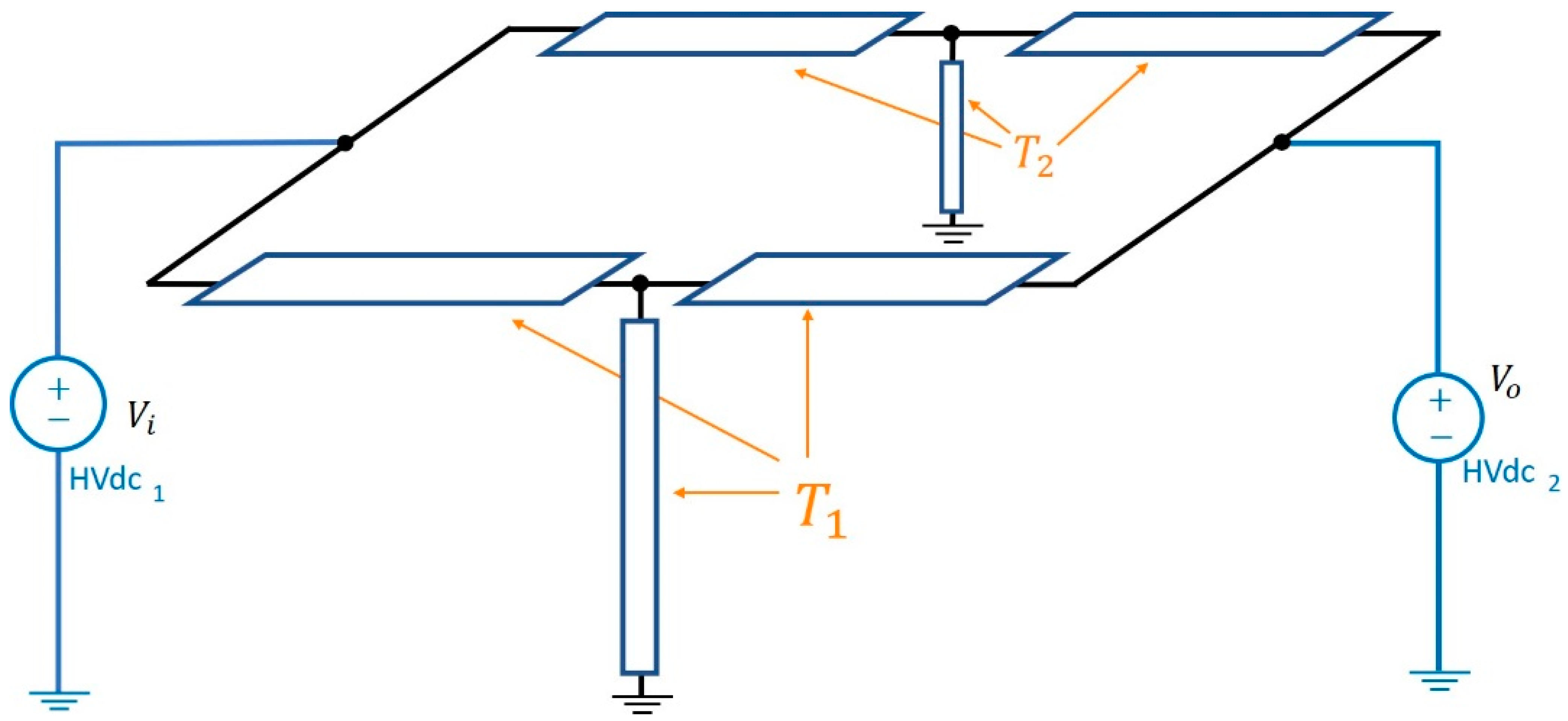
In this paper, a decoupled control strategy for a dc-dc converter intended for MT-HVdc applications is presented. The topology has been called double-T since it is built with two T-structures (see Figure 2). The proposed MMC operating with the presented control method exhibits the following features: no common-mode voltage at the converter output, the minimum number of cells to build the topology, and null ac components in the input current. The operating principle of the converter is described in detail as well as the proposed control strategy. Simulation results are presented to validate the control method and a sensitivity analysis is carried out to evaluate its performance under variations of the converter parameters.
The remainder of the paper is organized as follows. In Section 2 the mathematical model of the converter is presented. Section 3 describes the operating principle of the topology. The control strategy proposed is derived in Section 4 whereas the simulation results are presented in Section 5. In Section 6 Brief Sensitive Analysis is presented. Finally, the conclusions are stated in Section 7.

2. Converter Model

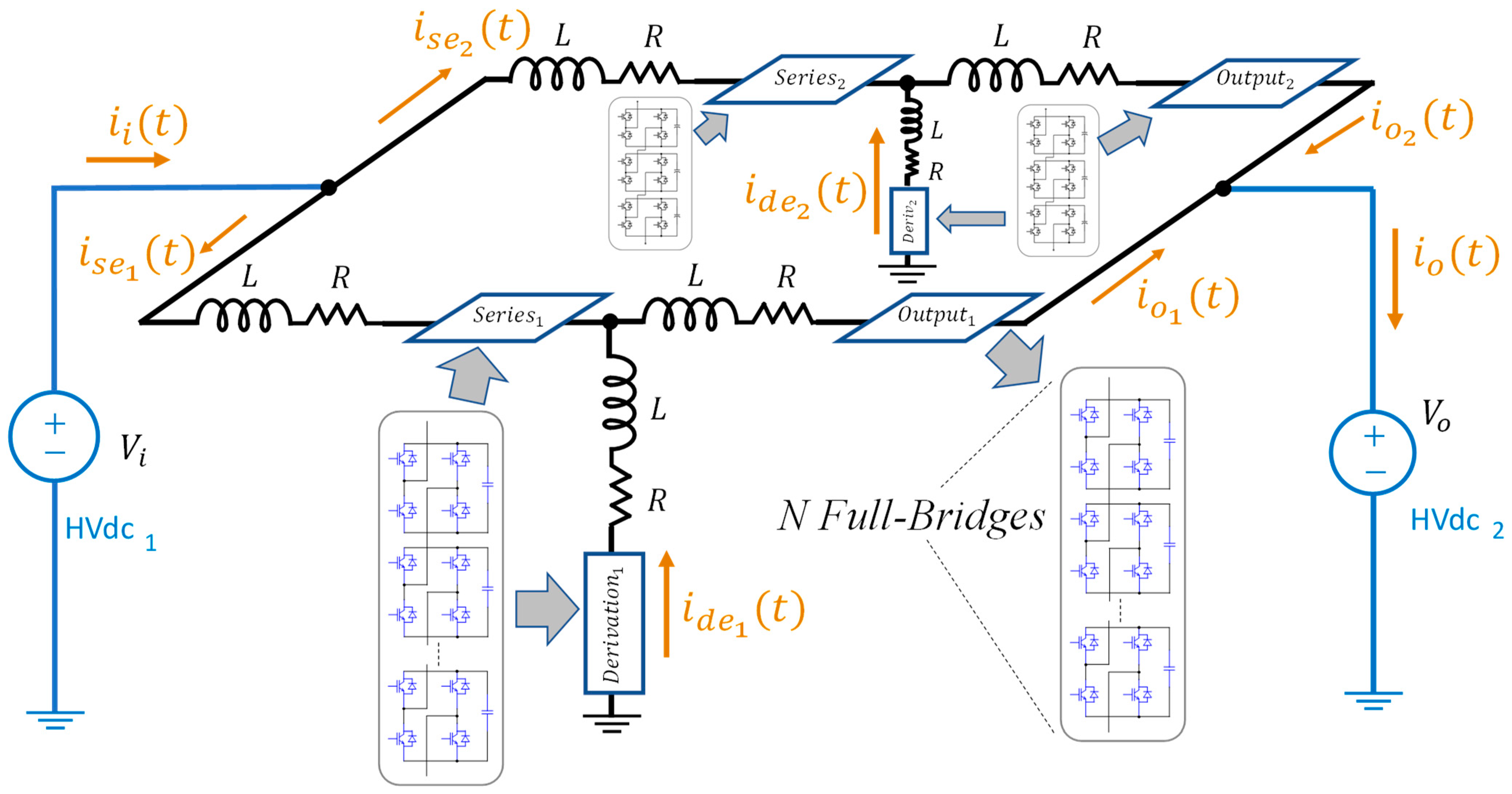
A schematic of the converter is shown in Figure 3. The converter is built with two T-structures ( T 1 and T 2 ) with three arms each. In turn, each arm is built with an inductor L and N cascaded H-bridges named series, derivation, and output stacks. The use of H-bridges in the stacks allows the possibility to operate with bidirectional power flow. Moreover, the inductors are required to couple the ac voltage components produced by each stack for current control purposes. The resistor R represents the equivalent resistance of the inductor and each T-structure is grounded through a derivation stack.
Figure 4 shows the average model of the converter in terms of the voltages and currents in each arm of the topology. Time-varying voltages v s e 1 , 2 t , v d e 1 , 2 t , and v o 1 , 2 t are produced by stacks series, derivation, and output, respectively. These time-varying voltages are dependent on the arm currents i s e 1 , 2 t , i d e 1 , 2 t , and i o 1 , 2 t , respectively. V i is the dc input voltage. V o is the converter output voltage which has a dc component and harmonics multiple of the switching frequency. In an MT-HVdc grid, V o is another terminal and can deliver power to V i .
Applying voltage and current laws to the meshes, then the main equations defining the average model can be derived:
V i = L d i s e 1 t d t L d i d e 1 t d t + R i s e 1 t i d e 1 t + v s e 1 t + v d e 1 t
V i = L d i s e 2 t d t L d i d e 2 t d t + R i s e 2 t i d e 2 t + v s e 2 t + v d e 2 t
0 = L d i d e 1 t d t + L d i o 1 t d t + R i d e 1 t + i o 1 t v d e 1 t + v o 1 t + V o
0 = L d i d e 2 t d t + L d i o 2 t d t + R i d e 2 t + i o 2 t v d e 2 t + v o 2 t + V o
i d e 1 t = i o 1 t i s e 1 t
i d e 2 t = i o 2 t i s e 2 t
i i t i d e 1 t i d e 2 t + i o t = 0
The voltages v s e 1 , 2 t , v d e 1 , 2 t and v o 1 , 2 t are defined in (8)–(10) where S i , s e 1 , 2 t , S i , d e 1 , 2 t and S i , o 1 , 2 t are the switching functions of each sub-module (H-bridge) of each stack of the topology. The value of the switching functions can be either −1, 0, or 1. Finally, C i are the capacitors of each sub-module.
v s e 1 , 2 t = j = 1 2 i = 1 N 1 C i i s e j t · S i , s e j t   d t
v d e 1 , 2 t = j = 1 2 i = 1 N 1 C i i d e j t · S i , d e j t   d t
v o 1 , 2 t = j = 1 2 i = 1 N 1 C i i o j t · S i , o j t   d t
From (1)–(7) it is possible to obtain the expressions for the instantaneous currents. Let x t = i o 1 t   i o 2 t   i s e 1 t   i s e 2 t T be the state vector of independent currents and u t = v s e 1 t   v s e 2 t   v d e 1 t   v d e 2 t   v o 1 t   v o 2 t T the control variables vector, the state-space model is given by:
d d t i o 1 ( t ) i o 2 ( t ) i s e 1 ( t ) i s e 2 t = R L i o 1 ( t ) i o 2 ( t ) i s e 1 ( t ) i s e 2 t + 1 3 L 1 0 1 0 2 0 0 1 0 1 0 2 2 0 1 0 1 0 0 2 0 1 0 1 v s e 1 ( t ) v s e 2 ( t ) v d e 1 ( t ) v d e 2 t v o 1 t v o 2 t + V i 2 V o V i 2 V o 2 V i V o 2 V i V o

3. Operating Principle

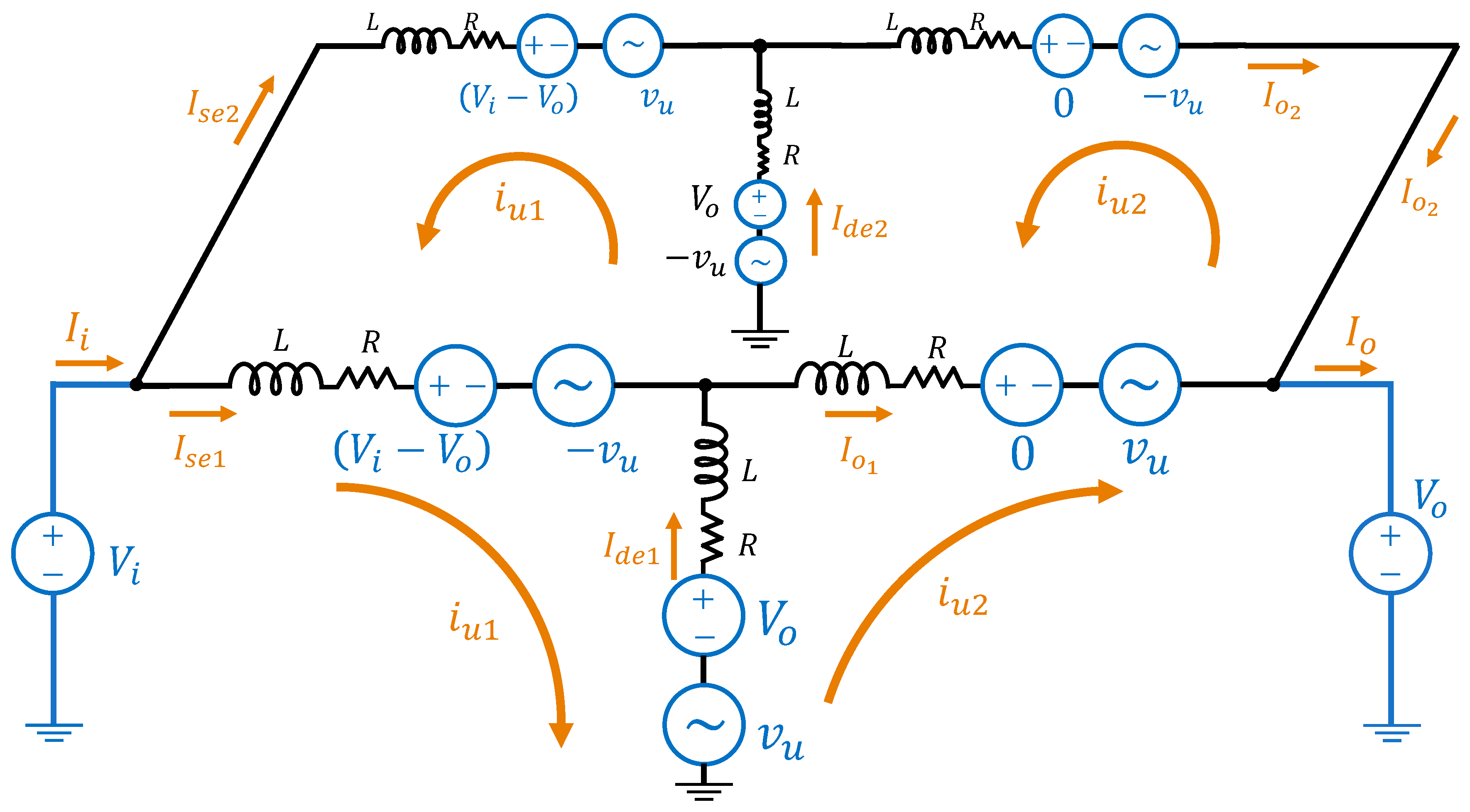
This work considers an approach based on the energy balance between the stacks of the converter. To achieve this balance ac and dc voltages and currents are employed to transfer energy to and from the different stacks. Figure 5 shows a simplified model using dc voltages V s e 1 , 2 , V d e 1 , 2 , V o 1 , 2 and ac voltages v s e 1 , 2 , v d e 1 , 2 , v o 1 , 2 that are produced by each stack, under steady-state operation. The dc voltages are obtained by applying voltage law to the arms of the topology; their values are V s e 1 , 2 = ( V i V o ) and V d e 1 , 2 = V o . For control purposes the dc voltages of the output stacks are zero. If V o 1 , 2 = 0 , the energy transferred by the output stacks due to dc components is minimized, and it is associated mainly to ac voltages and currents.
The ac voltages v s e 1 , 2 , v d e 1 , 2 , v o 1 , 2 have sinusoidal waveform as ± v u = ± V u sin 2 π f c t , where f c is a fundamental frequency. The sign of V u depends on the control objective and on the circulating current, in this case v s e 1 = v u , v s e 2 = v u , v d e 1 = + v u , v d e 2 = + v u , v o 1 = + v u and v o 2 = v u (see Figure 5). These ac voltages are intended to interact with the circulating ac currents i u 1 and i u 2 to achieve the energy balance of the converter.
The ac circulating currents can be expressed as i u 1 = I u 1 sin 2 π f c t and i u 2 = I u 2 sin 2 π f c t . These currents are aimed to allow the energy balance of the derivation ( i u 1 ) and output ( i u 2 ) stacks. Additionally, dc currents I s e 1 , 2 ,   I d e 1 , 2 ,   I o 1 , 2 circulate in all arms of the topology. The dc currents I s e 1 , 2 allow the energy balance of series stacks. Using expressions (1)–(7), neglecting the series equivalent resistance R of the inductor L and neglecting the product ω L which is comparatively small with respect to the product V I , it is possible to calculate the power equations of each stack as defined in (12)–(17). With the operating principle of the topology and the model defined in Section 2, the control strategy can now be derived as presented in Section 4.
P s e 1 = d W ¯ s e 1 d t = v s e 1 t · i s e 1 t d t = V i V o I s e 1 v u   i u 1
P d e 1 = d W ¯ d e 1 d t = v d e 1 t · i d e 1 t d t = V o I d e 1 + v u   i u 1 i u 2
P o 1 = d W ¯ o 1 d t = v 01 t · i o 1 t d t = v u   i u 2
P s e 2 = d W ¯ s e 2 d t = v s e 2 t · i s e 2 t d t = V i V o I s e 2 v u   i u 1
P d e 2 = d W ¯ d e 2 d t = v d e 2 t · i d e 2 t d t = V o I d e 2 v u   i u 1 + i u 2
P o 2 = d W ¯ o 2 d t = v o 2 t · i o 2 t d t = v u   i u 2

4. Control of the Double-T Converter

The control strategy is based on the average energy balance of all arms of the converter. The control scheme is composed by three stages: average energy control on each stack; current control with references obtained in the energy control; and stack internal control for the equalization of the dc-link voltage in each submodule.
A. 
Energy Balance of Stacks
Using expressions (1)–(4) and (11) and knowing that the independent currents of the topology are four, the control system is designed. Taking into account the energy balance approach, the energy of the series stack is controlled by I s e (see (12) and (15)) via a proportional–integral (PI) controller. For derivation stacks, the control action is performed by the ac current i u 1 whereas for output stacks, the energy control is carried out by the ac current i u 2 . It should be noted in Figure 5 that i u 1 and i u 2 circulate through both T-structures. Therefore, for the energy control of the converter, there are four PI controllers.
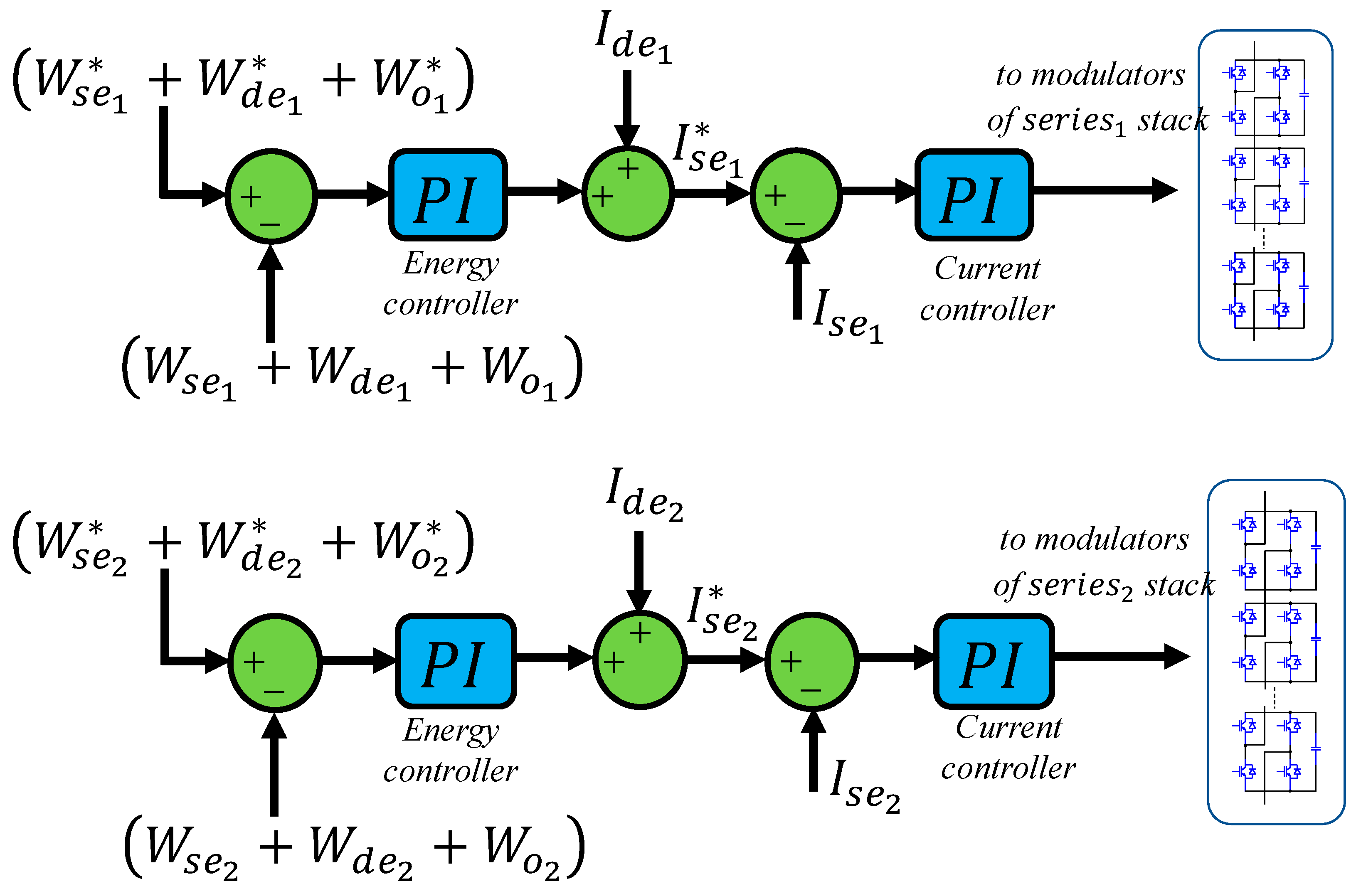
To impose the dc currents I s e 1 and I s e 2 from energy series1,2 controllers, another two PI controllers are used. As the energy control loops and the current control loops are nested, in this work they are decoupled using natural frequencies ω n of the controllers in a ratio of 1/70. The natural frequency of the series1,2 energy controllers is ω n e and the natural frequency of the current controllers is ω n c , then ω n c / ω n e = 70 . Figure 6 shows the control scheme for the energy balance of the series stacks.
To impose alternating currents i u 1 and i u 2 from energy controllers in derivation stacks, proportional–resonant ( P R ) controllers are used. In this work, the frequency used for i u 1 and i u 2 is f c = 500   Hz . This frequency should consider the “trade-off” between switching losses in the H-bridges and the dynamic response in the derivation energy balance controllers. Additionally, in this work, for the proposed operating point, the magnitude of v u is constant as V u = 0.7 V o . The value of V u is fundamental for the energy control of the derivation and output stacks. It is desired for V u to be high so that the dynamics of the control are fast, but it must not exceed the maximum output voltage to avoid overmodulation and the consequent voltage distortion. For the simulation study V u = 9.1   kV . Since the output direct voltage is V o = 13 k V D C , then V a r m = 13   kV + 9.1   kV = 22.1   kV is within the value that the converter arm can deliver. The maximum value to be delivered by the arm is V a r m m a x = 3   kV · 8 = 24   kV . Figure 7 shows the energy balance control scheme of the converter stacks.
B. 
Intra-Stacks Voltage Balance
The balance of the dc-links voltages of each stack is carried out by exchanging power between a quadrature current i q that circulates in addition to the energy balance currents. This current can be defined as i q = I q sin ω c t + π / 2 and is phase-shifted 90° with respect to i u 1 and i u 2 . Then, i u 1 + i q and i u 2 + i q are the currents circulating internally in the converter. Moreover, in each sub-module there is a voltage v b a l = V b a l sin ω c t + π / 2 that is in phase with the current i q . This allows exchanging power and generating the internal balance of the stacks keeping the dc-links of the N sub-modules with the same voltage. This voltage balance controller is based on a proportional (P) controller that receives the average value of the N dc-links voltages. The controller output is multiplied by sin ω c t + π / 2 and V b a l N is then generated. Finally, as i q is in quadrature with respect to the currents i u 1 and i u 2 , the intra-stack balance acts decoupled with respect to the energy control.
C. 
Decoupling Energy Balance Control
According to Equations (12)–(14), if these expressions are added, then (18) is obtained. In the same way, if (15)–(17) are added, the expression (19) is obtained.
P s e 1 + P d e 1 + P o 1 = V i V o I s e 1 V o I d e 1
P s e 2 + P d e 2 + P o 2 = v u   i u 2
Equations (18) and (19) are used to design the series stack energy controllers. The dc currents I d e 1 , 2 are added to obtain a feedforward compensation (see Figure 7). This leads to an improved energy balance dynamic of the dc-links of the series stacks. In the same way for the design of the derivation stacks energy control loops, if the (13), (14), (16), and (17) are added, the result is (20). In Figure 7 the implementation of the control strategy can be seen. For the control design of output stacks energy loops ( o u t p u t 1 and o u t p u t 2 ), as there is no power transfer of DC components, this decoupling principle does not apply.
P d e 1 + P o 1 + P d e 2 + P o 2 = 2 v u i u 1 V o I d e 1 + I d e 2

5. Simulations Results

Simulations are carried out considering the parameters in Table 1. Since 8 sub-modules per stack are used, the topology comprises a total of 48 H-bridges. The input and output voltage values have been defined for a typical MVdc distribution system.
Since the focus of this paper is on the control strategy for the double-T topology, the design aspects of the converter are not addressed in detail. However, general design procedures reported in [32,34,35] were followed.
Regarding the nomenclature used to show the results, the capacitor of the first H-bridge of the series1,2, derivation1,2, and output1,2 stacks will be called v c 1 s e 1 , 2 , v c 1 d e 1 , 2 and v c 1 o 1 , 2 , respectively.
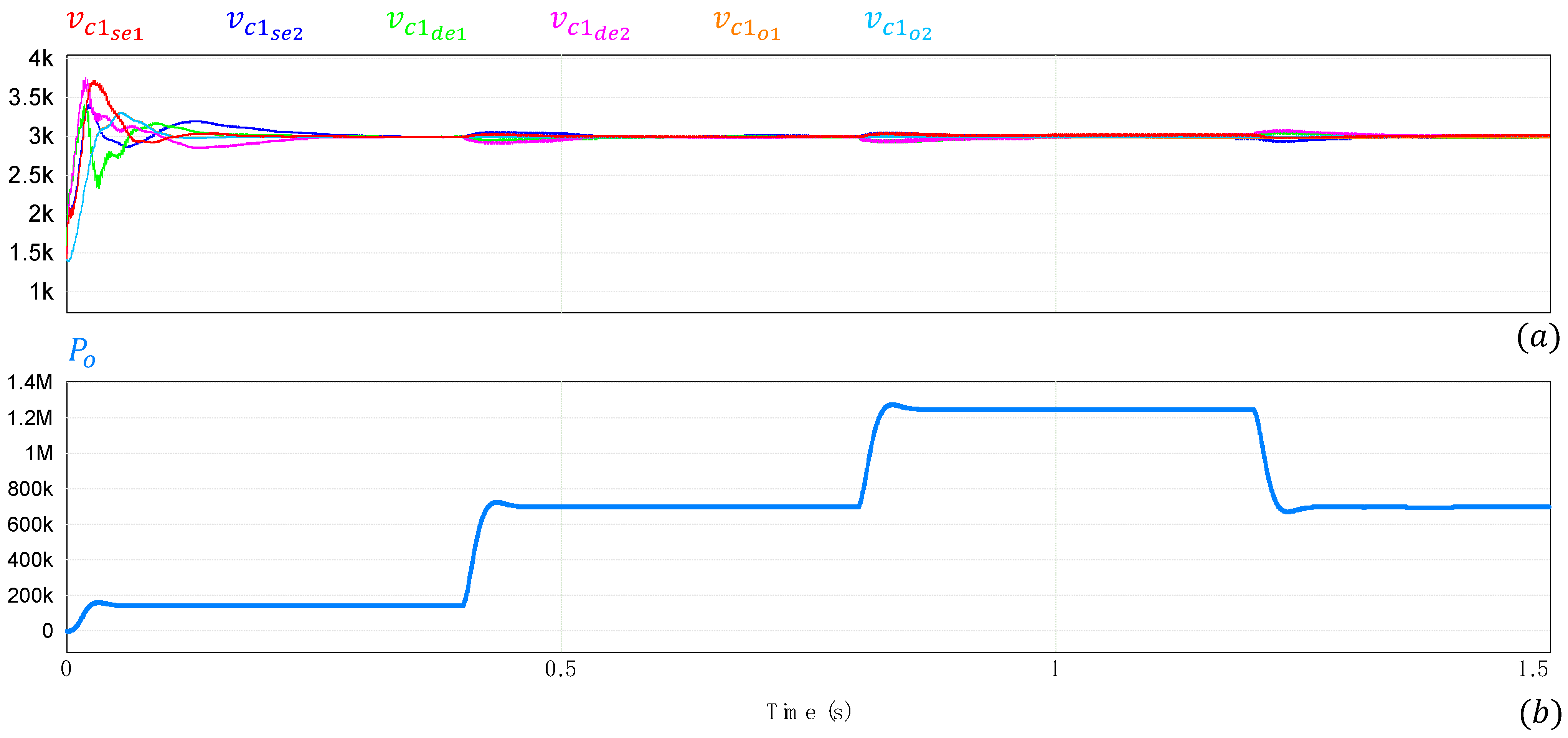
In the first test, simulations for load changes applied at t = 0.4 s, t = 0.8 s, and t = 1.2, are performed. Figure 8a shows one dc-link voltage per stack. As can be seen, the energy balance controller responds satisfactorily and very small variations in the dc-link voltages are obtained when the load changes. The voltage reference for all the dc-links has been set to 3 kV. Figure 8b shows the output power. From 0.8 to 1.2 s the output power is nominal.
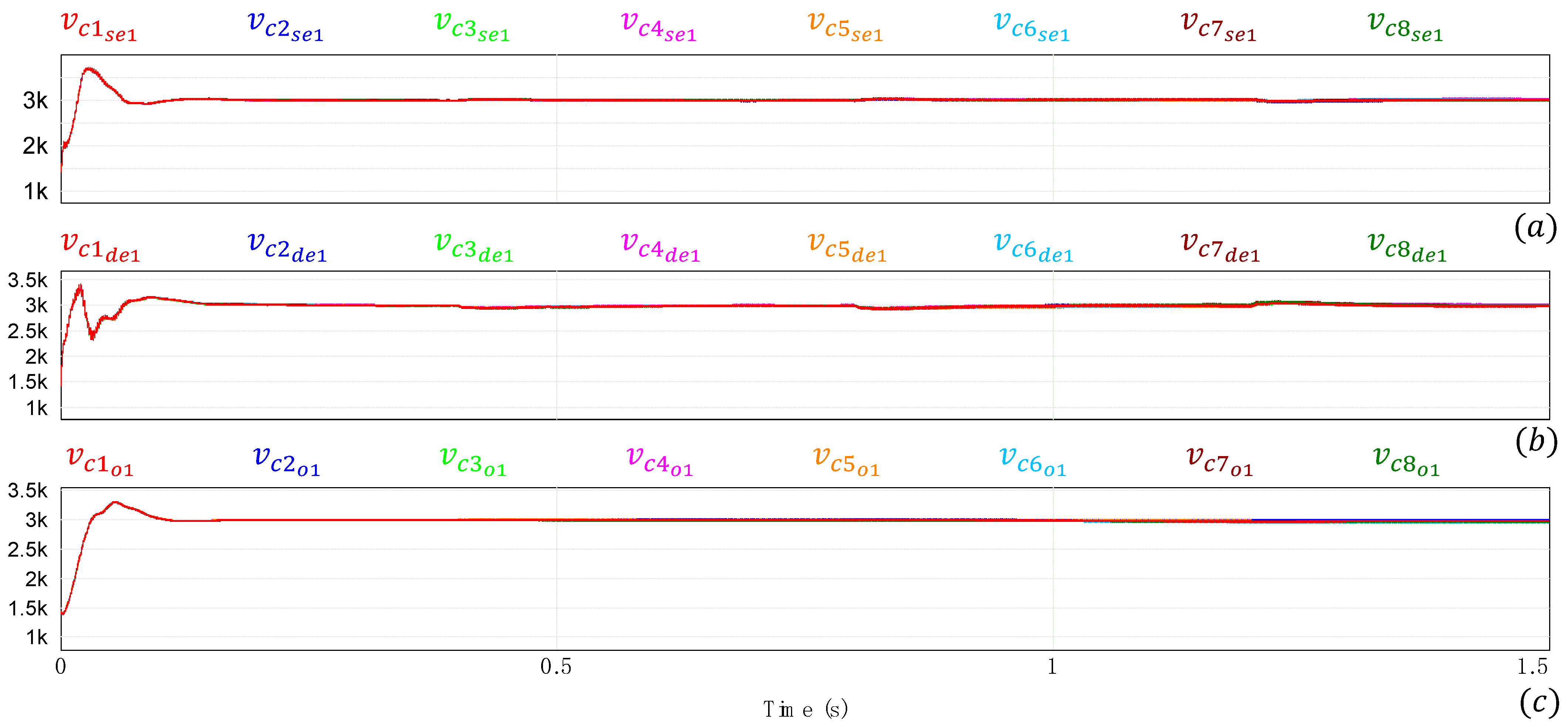
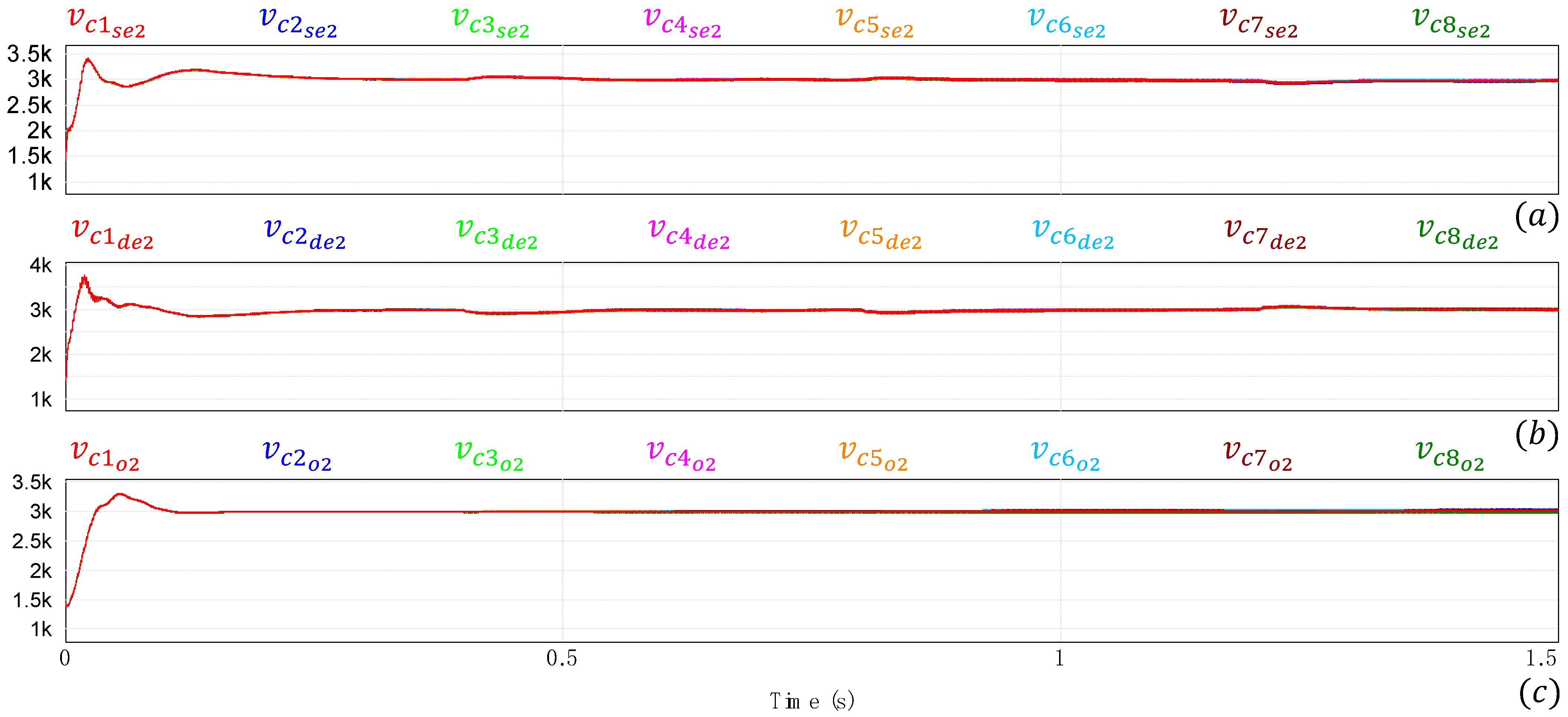
Figure 9 shows the 24 voltage waveforms of the dc-links of the T 1 structure whereas Figure 10 shows the dc-link voltages associated with the T 2 structure. An accurate response of the control scheme can be appreciated, with a minimum variation on the dc-link voltages when the load varies.
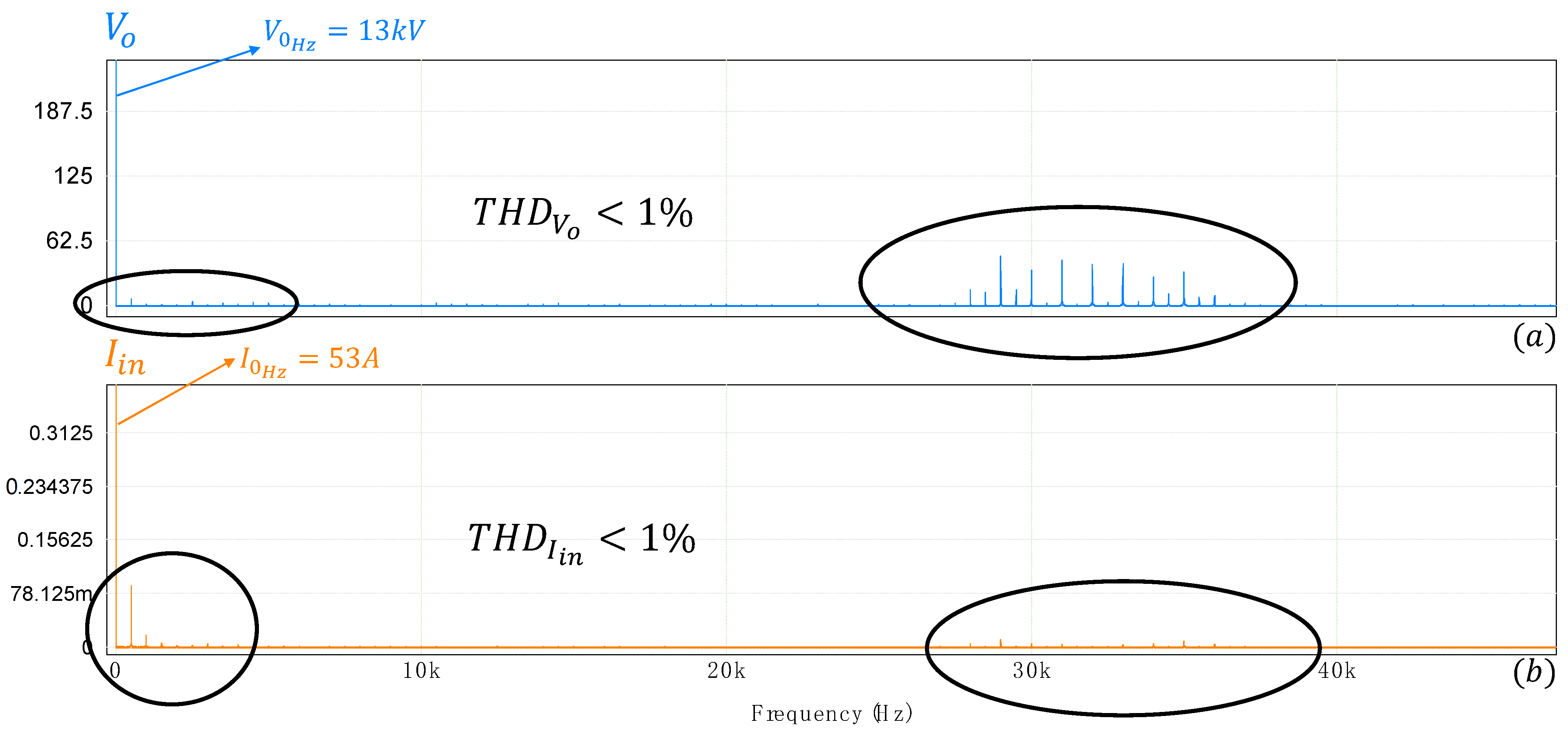
The converter output voltage and input current are shown in Figure 11, both presenting very low ripple. The spectra associated to these waveforms are shown in Figure 12. In both waveforms, the THD is lower than 1% with respect to the fundamental frequency, which in this case is 0 Hz. The average voltage value is V o 0 H z = 13   kV and the average current is I i n 0 H z = 53   A . As the number of sub-modules per stack are 8 and the switching frequency is 2   kHz , the harmonic components appear around 32   kHz (since the H-bridge doubles the equivalent switching frequency).
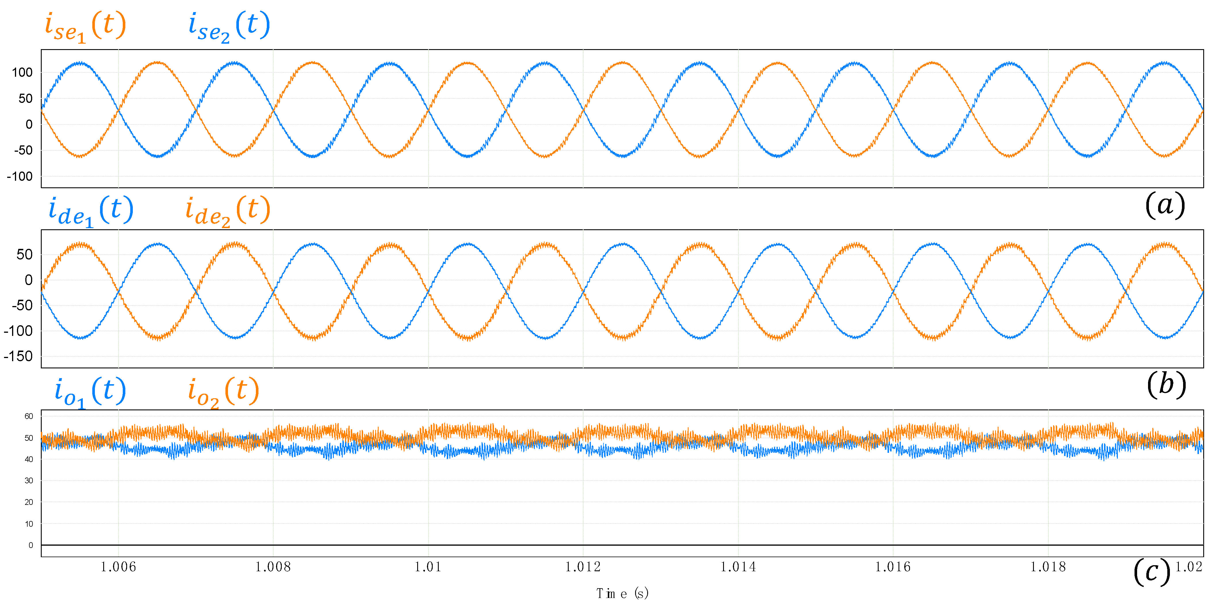
Figure 13 shows the currents of each converter arm. The currents in the series and derivation stacks are shown in Figure 13a,b, respectively. It can be noted that these currents have both ac and dc components. On the other hand, the current in the output stacks in Figure 13c is mainly dc with a small ac component. It is important to note that the currents i s e 1 and i s e 2 must be phase-shifted 180° so that the converter input current I i n has negligible ac component (see Figure 11b).
Figure 14 shows results for power variation and changes in the dc-link voltage reference. One dc-link voltage per stack is shown in Figure 14a and the output power is presented in Figure 14b. At t = 0.5 s a change in the reference of the dc-link voltages from 3 kV to 3.6 kV is applied. The opposite change is applied at t = 0.8 s. Good dynamic response of the dc-link voltages in every stack can be observed.
Figure 15 shows results for variations in the input and output voltages. In the case of the output voltage, the control reference is varied. Figure 15a shows the waveforms of one dc-link voltage per stack. Changes in the output voltage reference take place at t = 0.4 s and t = 0.8 s, whereas a change in the input voltage is applied at t = 0.6 s. In every input/output voltage variation applied, the fast and accurate response of the dc-link voltage control system can be observed.

6. Brief Sensitivity Analysis

A study to validate the performance of the control system under changes in parameters of the converters is carried out. Variations of the capacitances and inductances of the converters are considered, and the parameters of the controllers are not changed.

6.1. Case 1

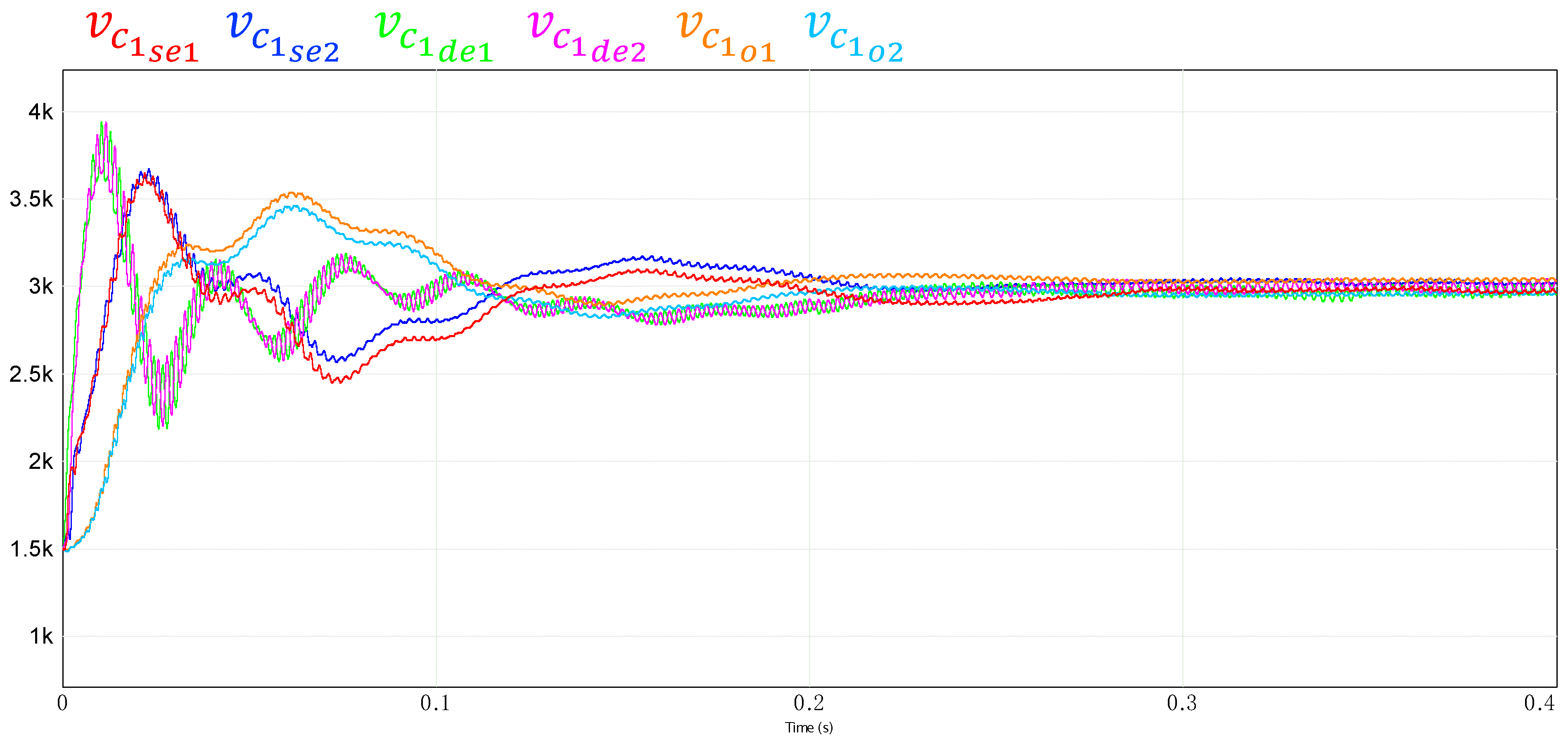
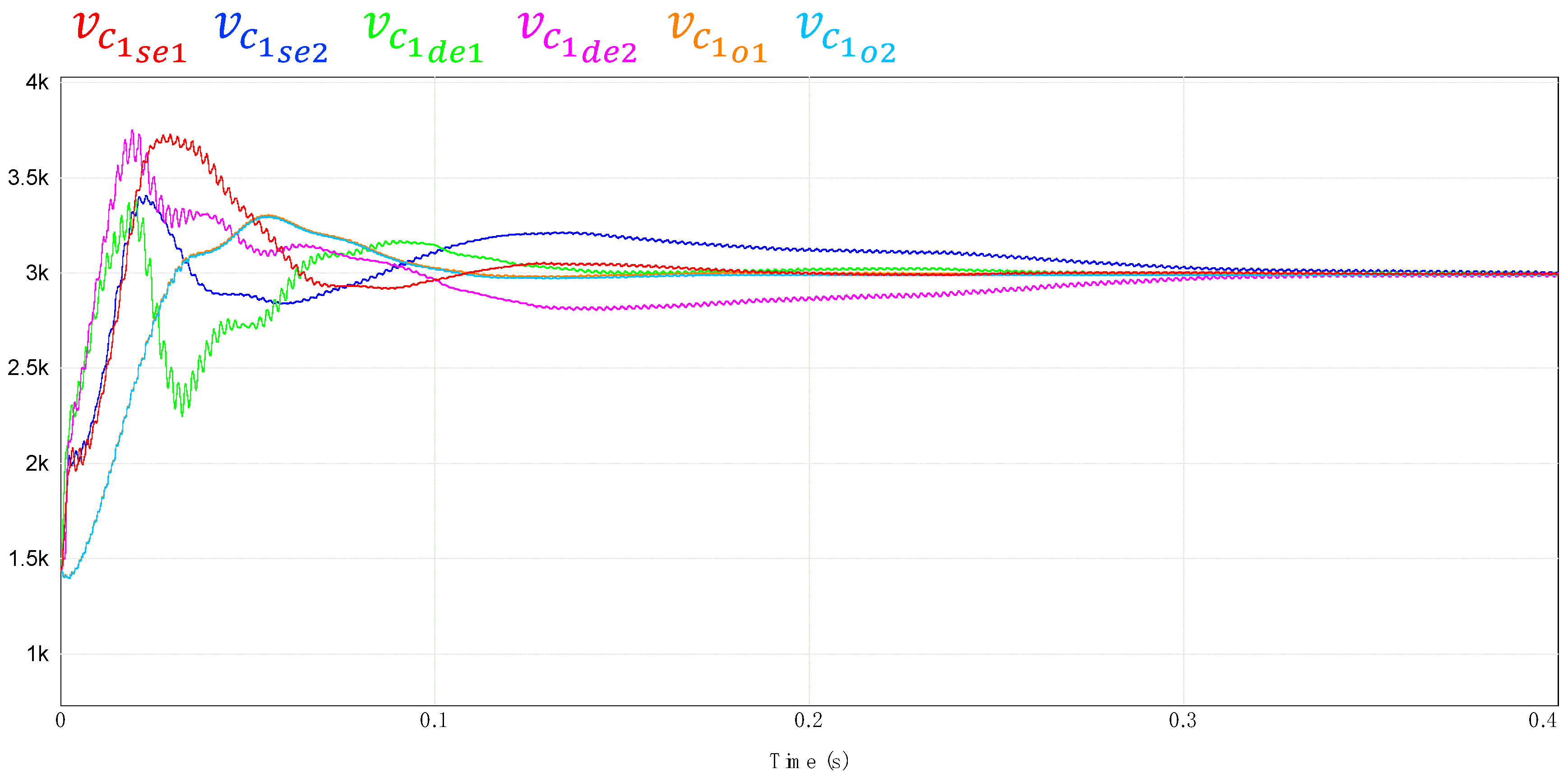
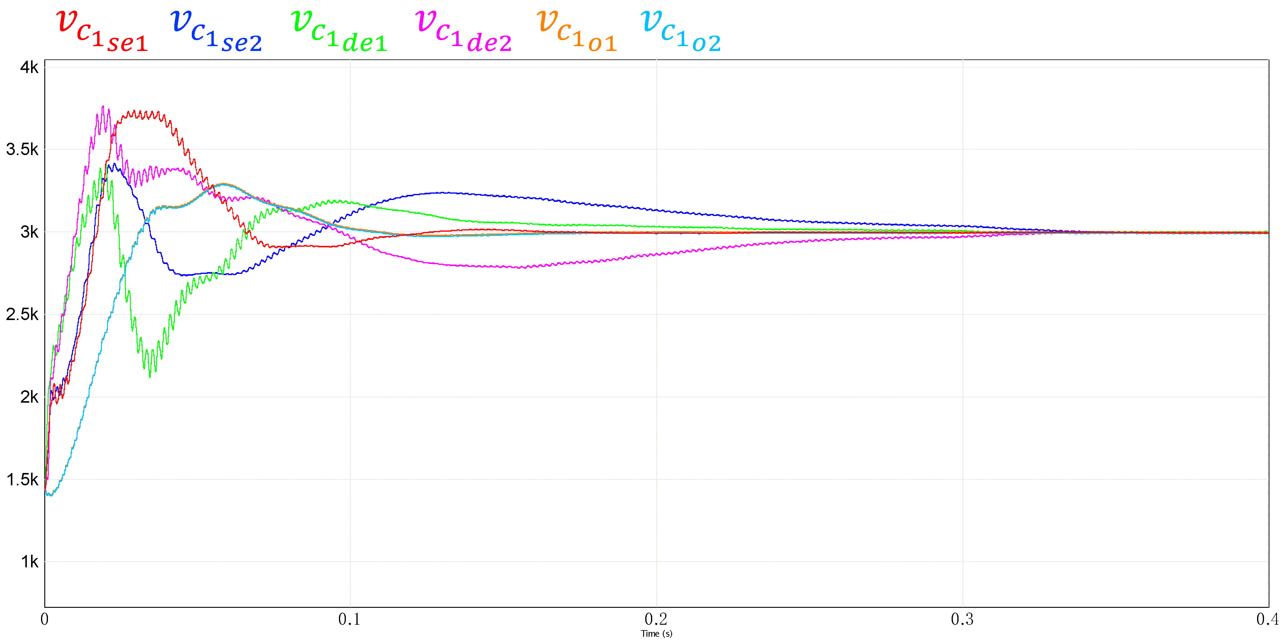
The value of the capacitors are set to C s e 1 = 1   mF , C s e 2 = 0.99   mF , C d e 1 = 1   mF , C d e 2 = 1.01   mF , C o 1 = 1   mF , and C o 2 = 1.01   mF . It should be mentioned that all the capacitors in a single arm are equal. The dc-link voltage reference is 3   kV and the converter operates with nominal load.
Figure 16 shows the dc-link voltages obtained. As can be seen, the control response is still accurate reaching the reference in short time and without error in steady state.

6.2. Case 2

In this second analysis, the values of the capacitors are: C s e 1 = 0.98   mF , C s e 2 = 1.02   mF , C d e 1 = 1   mF , C d e 2 = 1.02   mF , C o 1 = 0.98   mF , and C o 2 = 1.02   mF . The results are shown in Figure 17. Again, a good response of the control system and zero steady-state error are obtained.

6.3. Case 3

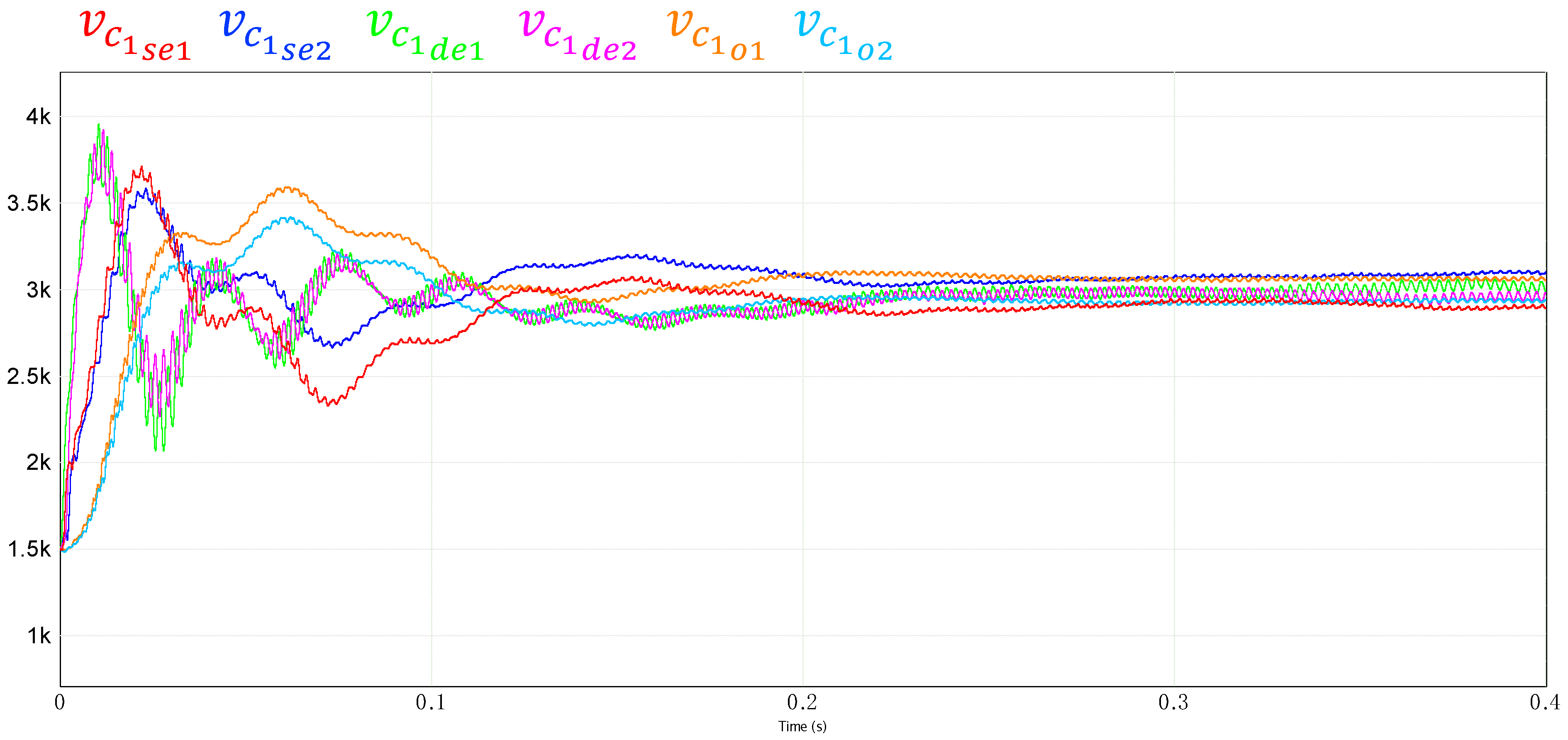
In this third analysis, the capacitor values are: C s e 1 = 0.9   mF , C s e 2 = 1.1   mF , C d e 1 = 0.95   mF , C d e 2 = 1.05   mF , C o 1 = 0.9   mF , and C o 2 = 1   mF . The dc-link voltage waveforms obtained are shown in Figure 18. In this case, the variation of the parameters has been in some arms more than 10% of the original value and certain steady-state errors can now be observed.
In the following cases 4, 5, and 6, the effect on the control system due to variations in the inductances is analyzed.

6.4. Case 4

In this first inductance variation scenario, the values of the inductors are set to L s e 1 = 2.51   mH , L s e 2 = 2.5   mH , L d e 1 = 2.49   mH , L d e 2 = 2.51   mH , L o 1 = 2.49   mH , and L o 2 = 2.5   mH . The dc-link voltages are presented in Figure 19 where a proper dynamic response and null steady-state error are appreciated.

6.5. Case 5

The values of the inductors are: L s e 1 = 2.45   mH , L s e 2 = 2.55   mH , L d e 1 = 2.46   mH , L d e 2 = 2.54   mH , L o 1 = 2.47   mH , and L o 2 = 2.5   mH , and the dc-link voltages are presented in Figure 20. Once again, the control responds properly and there is no error in the steady state.

6.6. Case 6

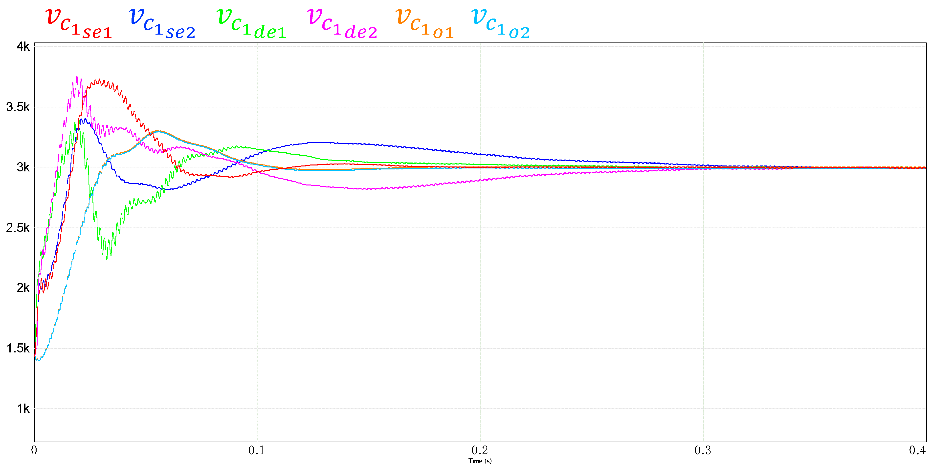
Finally, the inductor values are defined as: L s e 1 = 2.3   mH , L s e 2 = 2.65   mH , L d e 1 = 2.4   mH , L d e 2 = 2.45   mH , L o 1 = 2.6   mH , and L o 2 = 2.7   mH . For this condition, the results are shown in Figure 21 where a response similar to cases 4 and 5 is obtained.
On the other hand, variations of the inductor equivalent resistance of up to 10% of its original value have also been simulated, but the results showed no variations in the dc-link voltages, then they are not presented in this work.

7. Conclusions

The control strategy presented in this work allows us to balance the energy of the converter arms by means of circulating ac and dc currents. The ac currents circulate only inside the converter not being reflected in the input or output of the topology. The ac current flow through T 2 -structure is the same that in T 1 -structure, this allows us to obtain an input current with minimum harmonic content. Moreover, due to the control strategy, the output voltage has also a very low ripple. These characteristics are fundamental in HVdc systems since they are not designed to manage ac variables.
On the other hand, the sensitivity analysis shows that small variations of the converter parameters do not affect the performance of the control system.
The decoupling of the control allows us to reduce the impact of power changes on the output, as seen in the results. The presented topology operating with the proposed control strategy exhibits no common-mode alternating voltage component, which is an advantage and validates its possible use in HVdc or MVdc systems.

Author Contributions

Conceptualization, C.P., J.R. and R.P.; methodology, C.P.; software, C.P. and J.R.; validation, C.P. and R.V.; formal analysis, I.A. and W.J.; investigation, I.A. and W.J.; resources, R.V. and W.J.; writing—original draft preparation, C.P. and J.R.; writing—review and editing, R.P.; visualization, W.J.; supervision, J.R.; project administration, R. Villalobos; funding acquisition, R.P. and C.P. All authors have read and agreed to the published version of the manuscript.

Funding

This research was funded by the Chilean Agency of Research and Development, grant number “ANID FONDAP 15110019—PUENTE 1522A0006” and “DIUFRO Project support by Universidad de La Frontera grant number DI23-0011”.

Institutional Review Board Statement

Not applicable.

Informed Consent Statement

Not applicable.

Conflicts of Interest

The authors declare no conflict of interest.

References

  1. Liang, Y.; Ren, Y.; He, W. An Enhanced Current Differential Protection for AC Transmission Lines Connecting MMC-HVDC Stations. IEEE Syst. J. 2022, 17, 892–903. [Google Scholar] [CrossRef]
  2. Mehdi, A.; Kim, C.H.; Hussain, A.; Kim, J.S.; Hassan, S.J.U. A Comprehensive Review of Auto-Reclosing Schemes in AC, DC, and Hybrid (AC/DC) Transmission Lines. IEEE Access 2021, 9, 74325–74342. [Google Scholar] [CrossRef]
  3. Xu, X.; Meng, F.; Paramene, A.; Chen, X.; Qiu, L.; Zhou, W. Investigation on loss reduction strategies of single-core HVAC submarine cables. In Proceedings of the 22nd International Symposium on High Voltage Engineering (ISH 2021), Xi’an, China, 21–26 November 2021; pp. 44–48. [Google Scholar]
  4. Stanojev, O.; Garrison, J.; Hedtke, S.; Franck, C.M.; Demiray, T. Benefit Analysis of a Hybrid HVAC/HVDC Transmission Line: A Swiss Case Study. In Proceedings of the 2019 IEEE Milan PowerTech, Milan, Italy, 23–27 June 2019; pp. 1–6. [Google Scholar]
  5. Halder, T. Comparative Study of HVDC and HVAC for a bulk power Transmission. In Proceedings of the IEEE Power and Energy and Control (ICPEC), Dindigul, India, 6–8 February 2013; pp. 139–144. [Google Scholar]
  6. Meah, K.; Ula, S. Comparative Evaluation of HVDC and HVAC Transmission Systems. In Proceedings of the IEEE Power Engineering Society General Meeting, Tampa, FL, USA, 24–28 June 2007. [Google Scholar]
  7. Gumilar, L.; Sholeh, M.; Cahyani, D.E.; Kusumawardana, A.; Habibi, M.A.; Akhmadi, S.F. Comparison of Renewable Energy Output Power Transmission to Loads Via HVAC and HVDC. In Proceedings of the 2021 4th International Seminar on Research of Information Technology and Intelligent Systems (ISRITI), Yogyakarta, Indonesia, 16–17 December 2021; pp. 458–463. [Google Scholar]
  8. Apostolaki-Iosifidou, E.; Mccormack, R.; Kempton, W.; Mccoy, P.; Ozkan, D. Transmission Design and Analysis for Large-Scale Offshore Wind Energy Development. IEEE Power Energy Technol. Syst. J. 2019, 6, 22–31. [Google Scholar] [CrossRef]
  9. Hafeez, K.; Khan, S.A. High voltage direct current (HVDC) transmission: Future expectation for Pakistan. CSEE J. Power Energy Syst. 2019, 5, 82–86. [Google Scholar] [CrossRef]
  10. Migliori, M.; Lauria, S.; Michi, L.; Donnini, G.; Aluisio, B.; Vergine, C. Renewable sources integration using HVDC in parallel to AC traditional system: The Adriatic project. In Proceedings of the 2019 AEIT HVDC International Conference (AEIT HVDC), Florence, Italy, 9–10 May 2019; pp. 1–5. [Google Scholar]
  11. Wu, Y.; Yu, F.; Guo, J.; Shen, L. Research on the effects of different DC filter configurations in ±1100kV UHVDC transmission system. In Proceedings of the 16th IET International Conference on AC and DC Power Transmission (ACDC 2020), Online, 2–3 July 2020; pp. 758–761. [Google Scholar]
  12. Lange, J.; Neubert, R.; Alt, B.; Hussennether, V.; de Abreu, M.G.C. Innovative Converter Testing Technology and Overall Reliability and Availability Performance of HVDC Solutions. In Proceedings of the 2021 AEIT HVDC International Conference (AEIT HVDC), Genoa, Italy, 27–28 May 2021; pp. 1–6. [Google Scholar]
  13. Tecnología HVDC y su Integración al sen, Cigre-Chile, 2021. Available online: https://www.cigre.cl/2021/07/23/tecnologia-hvdc-y-su-integracion-al-sen/ (accessed on 1 February 2023).
  14. Sousa, T.; Santos, M.L.; Jardini, J.A.; Casolari, R.P.; Nicola, G.L.C. An evaluation of the HVDC and HVAC transmission economic. In Proceedings of the 2012 Sixth IEEE/PES Transmission and Distribution: Latin America Conference and Exposition (T&D-LA), Montevideo, Uruguay, 3–5 September 2012; pp. 1–6. [Google Scholar] [CrossRef]
  15. ABB and Aibel Technical News. Available online: https://www.4coffshore.com/news/abb-and-aibel-net-dogger-bank-bounty-nid14371.html (accessed on 1 February 2023).
  16. CIGRE Session 2022 28 August–02 September 2022 Paris, France. Available online: https://www.cigre.org/article/GB/news/the_latest_news/roadmaps-to-a-common-destination-decarbonization-of-energy-systems (accessed on 1 February 2023).
  17. Ma, K.; Annakkage, U.D.; Karawita, C. Development of a small-signal assessment tool for multi-terminal LCC schemes. In Proceedings of the 15th IET International Conference on AC and DC Power Transmission (ACDC 2019), Coventry, UK, 5–7 February 2019; pp. 1–7. [Google Scholar]
  18. Garces, A.; Sanchez, S.; Bergna, G.; Tedeschi, E. HVDC Meshed Multi-Terminal Networks for Offshore Wind Farms: Dynamic Model, Load Flow and Equilibrium. In Proceedings of the IEEE COMPEL, Stanford, CA, USA, 9–12 July 2017; pp. 1–6. [Google Scholar]
  19. Ambia, M.N.; Meng, K.; Xiao, W.; Al-Durra, A.; Dong, Z.Y. Adaptive Droop Control of Multi-Terminal HVDC Network for Frequency Regulation and Power Sharing. IEEE Trans. Power Syst. 2021, 36, 566–578. [Google Scholar] [CrossRef]
  20. Solhjoukhah, Z.; Egea-Alvarez, A.; Gomis-Bellmunt, O. Voltage Control of Offshore Load Connected to a Multi-Terminal HVDC Transmission System. In Proceedings of the 11th IET International Conference on AC and DC Power Transmission, Birmingham, UK, 10–12 February 2015; pp. 1–9. [Google Scholar]
  21. Alagab, S.M.; Tennakoon, S.; Gould, C. Comparison of Single-stage and Multi-stage Marx DC-DC converters for HVDC application. In Proceedings of the 2018 53rd International Universities Power Engineering Conference (UPEC), Glasgow, UK, 4–7 September 2018; pp. 1–6. [Google Scholar]
  22. Zhang, S.; Li, B.; Zhao, X.; Zhang, Y.; Wang, W.; Xu, D. A Transformerless Hybrid Modular Step-up DC/DC Converter for Bipolar and Symmetrical Monopolar HVDC Interconnection. In Proceedings of the 2019 4th IEEE Workshop on the Electronic Grid (eGRID), Xiamen, China, 11–14 November 2019; pp. 1–6. [Google Scholar]
  23. Liu, Y.; Lei, D.; Ning, Z.; Ren, Y.; Wang, Y.; Tian, J.; Wang, H.; Xu, R. A Novel Topology of Three-Port DC-DC Converter with Improved Carrier Phase-Shifted Control for MVDC Applictions. In Proceedings of the 2021 IEEE/IAS Industrial and Commercial Power System Asia (I&CPS Asia), Chengdu, China, 18–21 July 2021; pp. 74–78. [Google Scholar]
  24. Páez, J.D.; Frey, D.; Maneiro, J.; Bacha, S.; Dworakowski, P. Overview of DC–DC Converters Dedicated to HVdc Grids. IEEE Trans. Power Deliv. 2019, 34, 119–128. [Google Scholar] [CrossRef]
  25. Adam, G.P.; Gowaid, I.A.; Finney, S.J.; Holliday, D.; Williams, B.W. Review of dc-dc converters for multi-terminal hvdc transmission networks. IET Power Electron. 2016, 9, 281–296. [Google Scholar] [CrossRef] [Green Version]
  26. Cui, W.; Shao, S.; Zhang, J.; Li, Y.; Zhang, J. Bidirectional Modular Multilevel Resonant DC-DC Converter for Medium Voltage Power Conversion. In Proceedings of the 2020 IEEE Energy Conversion Congress and Exposition (ECCE), Detroit, MI, USA, 11–15 October 2020; pp. 4380–4385. [Google Scholar]
  27. Zhang, X.; Green, T.C. The Modular Multilevel Converter for High Step-Up Ratio DC–DC Conversion. IEEE Trans. Ind. Electron. 2015, 62, 4925–4936. [Google Scholar] [CrossRef] [Green Version]
  28. Shao, S.; Li, Y.; Sheng, J.; Li, C.; Li, W.; Zhang, J.; He, X. A Modular Multilevel Resonant DC–DC Converter. IEEE Trans. Power Electron. 2020, 35, 7921–7932. [Google Scholar] [CrossRef]
  29. Xiang, X.; Zhang, X.; Zhu, Y.; Chaffey, G.P.; Gu, Y.; Green, T.C. The Resonant Modular Multilevel DC Converters for High Step-ratio and Low Step-ratio Interconnection in MVDC Distribution Network. In Proceedings of the IECON 2019—45th Annual Conference of the IEEE Industrial Electronics Society, Lisbon, Portugal, 14–17 October 2019; pp. 5686–5693. [Google Scholar]
  30. Pineda, C.; Pereda, J.; Rojas, F.; Cerda, C.; Zhang, X.; Watson, A.J. Asymmetrical Triangular Current Mode (ATCM) for Bidirectional High Step Ratio Modular Multilevel Dc–Dc Converter. IEEE Trans. Power Electron. 2020, 35, 6906–6915. [Google Scholar] [CrossRef]
  31. Elgenedy, M.A.; Alhurayyis, I.; Elkhateb, A.; Ahmed, K.; Kroičs, K. A New DC-DC Converter Linking LCC-HVDC Transmission Networks. In Proceedings of the 2021 23rd European Conference on Power Electronics and Applications (EPE’21 ECCE Europe), Ghent, Belgium, 6–10 September 2021; pp. P.1–P.10. [Google Scholar]
  32. Vidal, R.; Belenguer, E.; Pesce, C.; Soto, D.; Pena, R.; Blasco-Gimenez, R.; Riedemann, J. Power flow control using a DC-DC MMC for HVdc grid connected wind power plants. In Proceedings of the IECON 2015—41st Annual Conference of the IEEE Industrial Electronics Society, Yokohama, Japan, 9–12 November 2015; pp. 005107–005112. [Google Scholar] [CrossRef]
  33. Klimczak, P.; Blaszczyk, P.; Jez, R.; Koska, K. Double wye Modular Multilevel Converter—Direct DC-DC topology. In Proceedings of the 8th IET International Conference on Power Electronics, Machines and Drives (PEMD 2016), Glasgow, UK, 19–21 April 2016; pp. 1–6. [Google Scholar]
  34. Shivashanker, K.; Janaki, M.; Thirumalaivasan, R. Design of Decoupled Current Controller for Back to Back Modular Multilevel Converter Based HVDC Transmission System. In Proceedings of the 2021 Innovations in Power and Advanced Computing Technologies (i-PACT), Kuala Lumpur, Malaysia, 27–29 November 2021. [Google Scholar]
  35. Oates, C. Modular multilevel converter design for VSC HVDC applications. IEEE J. Emerg. Sel. Top. Power Electron. 2014, 3, 505–515. [Google Scholar] [CrossRef]
Figure 1. Schematic of a multi-terminal HVdc system.
Applsci 13 03778 g001
Figure 2. Double-T topology, with two T-structures called T 1 and T 2 .
Applsci 13 03778 g002
Figure 3. Scheme of the double-T topology.
Applsci 13 03778 g003
Figure 4. Average model of the double-T topology.
Applsci 13 03778 g004
Figure 5. Simplified scheme of the topology with ac and dc voltages and circulating currents.
Applsci 13 03778 g005
Figure 6. Series stacks energy and current control scheme.
Applsci 13 03778 g006
Figure 7. Derivation and output stacks energy and current control scheme.
Applsci 13 03778 g007
Figure 8. (a) One dc-link voltage per stack. (b) Converter output power.
Applsci 13 03778 g008
Figure 9. T 1 dc-link voltages. (a) series1 stack. (b) derivation1 stack. (c) output1 stack.
Applsci 13 03778 g009
Figure 10. T 2 dc-link voltages. (a) series2 stack. (b) derivation2 stack. (c) output2 stack.
Applsci 13 03778 g010
Figure 11. (a) Output voltage. (b) Input current.
Applsci 13 03778 g011
Figure 12. (a) Output voltage spectra. (b) Input current spectra.
Applsci 13 03778 g012
Figure 13. (a) i s e 1 t and i s e 2 t currents. (b) i d e 1 t and i d e 2 t currents. (c) i o 1 t and i o 2 t currents.
Applsci 13 03778 g013
Figure 14. (a) One dc-link voltage per stack. (b) Converter output power (for for dc-links voltage control reference changes).
Applsci 13 03778 g014
Figure 15. (a) One dc-link voltage per stack. (b) Converter input voltage (c) Converter output voltage.
Applsci 13 03778 g015
Figure 16. Dc-link voltage waveforms for case 1.
Applsci 13 03778 g016
Figure 17. Dc-link voltage waveforms for case 2.
Applsci 13 03778 g017
Figure 18. Dc-link voltage waveforms for case 3.
Applsci 13 03778 g018
Figure 19. Dc-link voltage waveforms for case 4.
Applsci 13 03778 g019
Figure 20. Dc-link voltage waveforms for case 5.
Applsci 13 03778 g020
Figure 21. Dc-link voltage waveforms for case 6.
Applsci 13 03778 g021
Table 1. Simulation parameters.
DescriptionValue
Input voltage, H V D C 1 = V i n 23000   V
Output voltage, H V D C 2 = V o 13000   V
Rated output power, P o u t 1.25   MW
Dc-links capacitors, C s e 1 , 2 = C d e 1 , 2 = C o 1 , 2 1   mF
Arm inductances, L 2.5   mH
Series equivalent resistance of inductors, R 50   m
Dc-links reference voltage 3000   V
Frequency of ac circulating currents 500   Hz
Number of H-bridges per stack 8
Number of arms 6
Switching frequency, f s w 2   kHz
Disclaimer/Publisher’s Note: The statements, opinions and data contained in all publications are solely those of the individual author(s) and contributor(s) and not of MDPI and/or the editor(s). MDPI and/or the editor(s) disclaim responsibility for any injury to people or property resulting from any ideas, methods, instructions or products referred to in the content.