Brief Report

Capacitor-Less Low-Power Neuron Circuit with Multi-Gate Feedback Field Effect Transistor

Department of Electronic Engineering, Gangneung-Wonju National University, Gangneung 640-2387, Republic of Korea
*
Author to whom correspondence should be addressed.
Appl. Sci. 2023, 13(4), 2628; https://doi.org/10.3390/app13042628
Submission received: 29 January 2023 / Revised: 14 February 2023 / Accepted: 16 February 2023 / Published: 17 February 2023

Abstract

:
Recently, research on artificial neuron circuits imitating biological systems has been actively studied. The neuron circuit can implement an artificial neural network (ANN) capable of low-power parallel processing by configuring a biological neural network system in hardware. Conventional CMOS analog neuron circuits require many MOSFETs and membrane capacitors. Additionally, it has low energy efficiency in the first inverter stage connected to the capacitor. In this paper, we propose a low-power neuron circuit with a multi-gate feedback field effect transistor (FBFET) that can perform integration without a capacitor to solve the problem of an analog neuron circuit. The multi-gate FBFET has a low off-current due to its low operating voltage and excellent sub-threshold characteristics. We replace the n-channel MOSFET of the inverter with FBFET to suppress leakage current. FBFET devices and neuron circuits were analyzed using TACD and SPICE mixed-mode simulation. As a result, we found that the neuron circuit with multi-gate FBFET has a low subthreshold slope and can completely suppress energy consumption. We also verified the temporal and spatial integration of neuron circuits.

1. Introduction

Existing digital systems, such as computers, have been developed through computation using semiconductors and the integration of logic and memory devices. Digital systems based on the Von Neumann structure, which are based on the signal exchange between processing/logic devices and memory devices, have been used very successfully to date. Recently, there has been a surge in demand for processing numerous data at once, such as big data and Artificial Intelligence (AI), but the Von Neumann computing structure creates a bottleneck between computing units and data storage, leading to overall system performance degradation. Therefore, a new concept of a computing system for high energy efficiency and excellent performance is required to overcome the problems of existing Von Neumann computing systems. Various studies are being conducted with a different approach than used before, and among them, Spiking Neural Network (SNN) technology is a research technology that is inspired by biological principles to implement neural networks through it [1,2,3,4,5,6,7,8,9]. SNN is a technology that directly combines neurobiological mechanisms in neuroscience into AI and is known as the third-generation Artificial Neural Network (ANN) technology that utilizes time-based information encoding and time-based information processing, one of the main functions of the brain. SNN-based neuromorphic computing aims to efficiently mimic biological spiking neural network mechanisms by distributing synaptic operations and information storage through an event-based asynchronous spike motion mechanism across a number of relatively simple computing devices, neurons. These hardware-based spiking neural networks consist of numerous neuron circuits, and each neuron circuit plays the same role as a real biological neuron. Therefore, most of the power consumption is consumed when neurons make spikes. Therefore, it is important to reduce the power consumption of each neuron in order to reduce power consumption. However, most analog neuron circuits accumulate input signals using membrane capacitors. Additionally, most of the power is consumed in the first inverter step. The reason is that in the analog neuron circuit, the voltage of the capacitor increases only when the input signal is received, and the voltage of the first inverter increases slowly. If the voltage increases slowly, the time when the PMOS and NMOS are turned on simultaneously increases, and thus, a short circuit current (Isc) continues to flow from Vdd to ground. In addition, when the membrane capacitor is charged up to the switching voltage of the inverter, short-circuit current continues to flow through the first inverter without spikes, which can consume more power than when neurons discharge the capacitor after generating spikes. That is, conventional analog neuron circuits require many transistors and large capacitors to integrate neuron signals, which are problematic in scale. Additionally, whenever an input pulse is applied for a long time, the membrane potential gradually increases, generating Isc before threshold voltage (Vth) and consuming most of the energy in the first inverter step [10,11].
To solve these problems, a device with excellent steep switching characteristics and capable of replacing the role of a membrane capacitor should be used in neuron circuits. In this study, we adopted the FBFET as the device. The FBFET has a steep switching characteristic; therefore, it can suppress leakage current [12,13]. Additionally, the mechanism is similar to that of a transistor; therefore, it has excellent endurance characteristics and can be processed by a typical CMOS process. In addition, the device can replace the role of the membrane capacitor by storing electric charges in the floating body. By applying FBFET with these characteristics, we design a neuron circuit that can significantly reduce power consumption. The proposed neuron circuit solves leakage current and scale problems by adding a feedback device to the first inverter and replacing the membrane capacitor. Based on the measurement result of the fabricated FBFET, the simulation parameters were calibrated, and the multi-gate FBFET simulation structure was designed. The characteristics of FBFET were verified using SILVACO TCAD simulation, and transistors were applied to neuron circuits and compared with existing neuron circuits through SPICE simulation.

2. FBFET

2.1. FBFET Simulation Results and Characterisitcs

We configured the FBFET structure combined with PNPN body doping and two gates (Gate and Control Gate). Gate 1 adjusts the potential barrier height, and a control gate generates a potential well for electron accumulation. The device structure is designed by TCAD, and it is illustrated in Figure 1.
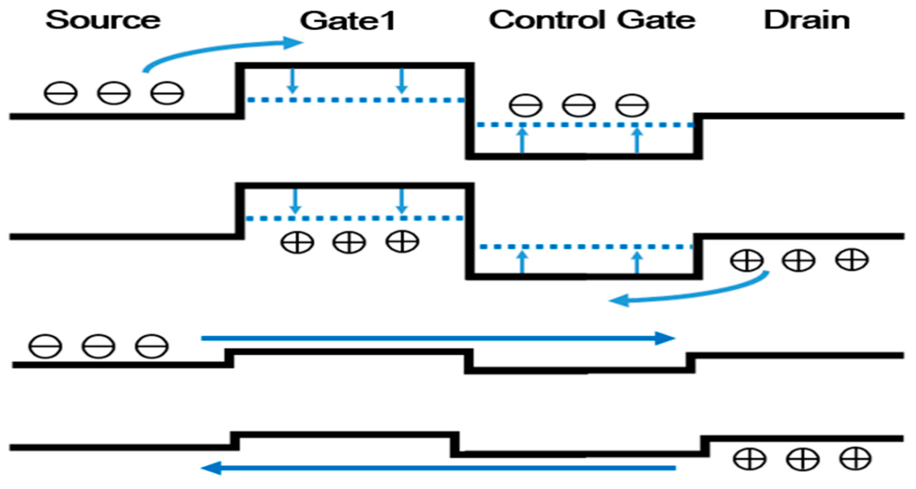
Figure 2 shows the mechanism of FBFET and its operating principle as followed [14,15,16,17,18].
  • Put in positive voltage to the control gate, and a potential well is created under the control gate to accumulate electrons.
  • Applying a positive bias to gate 1 lowers the potential barrier. Additionally, source electrons cross the potential barrier and accumulated in the potential well under the control gate.
  • The accumulated electrons lower the barrier height of the valence band on the drain, and then holes are accumulated in the p-body below the gate 1.
  • Likewise, the accumulated holes drop the potential barrier on the source, and the potential barriers become very low. Therefore, the current increases rapidly, and the FBFET turns on steeply.
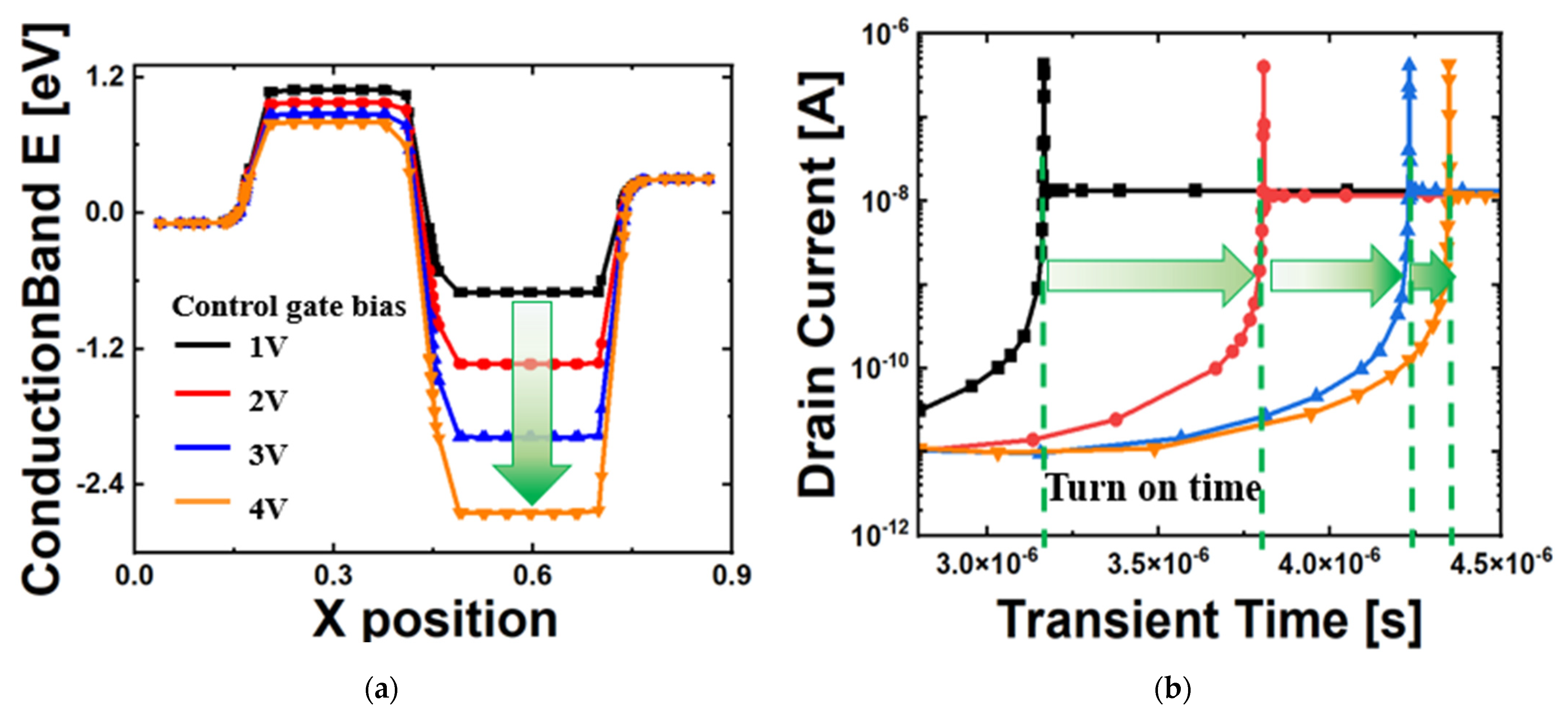
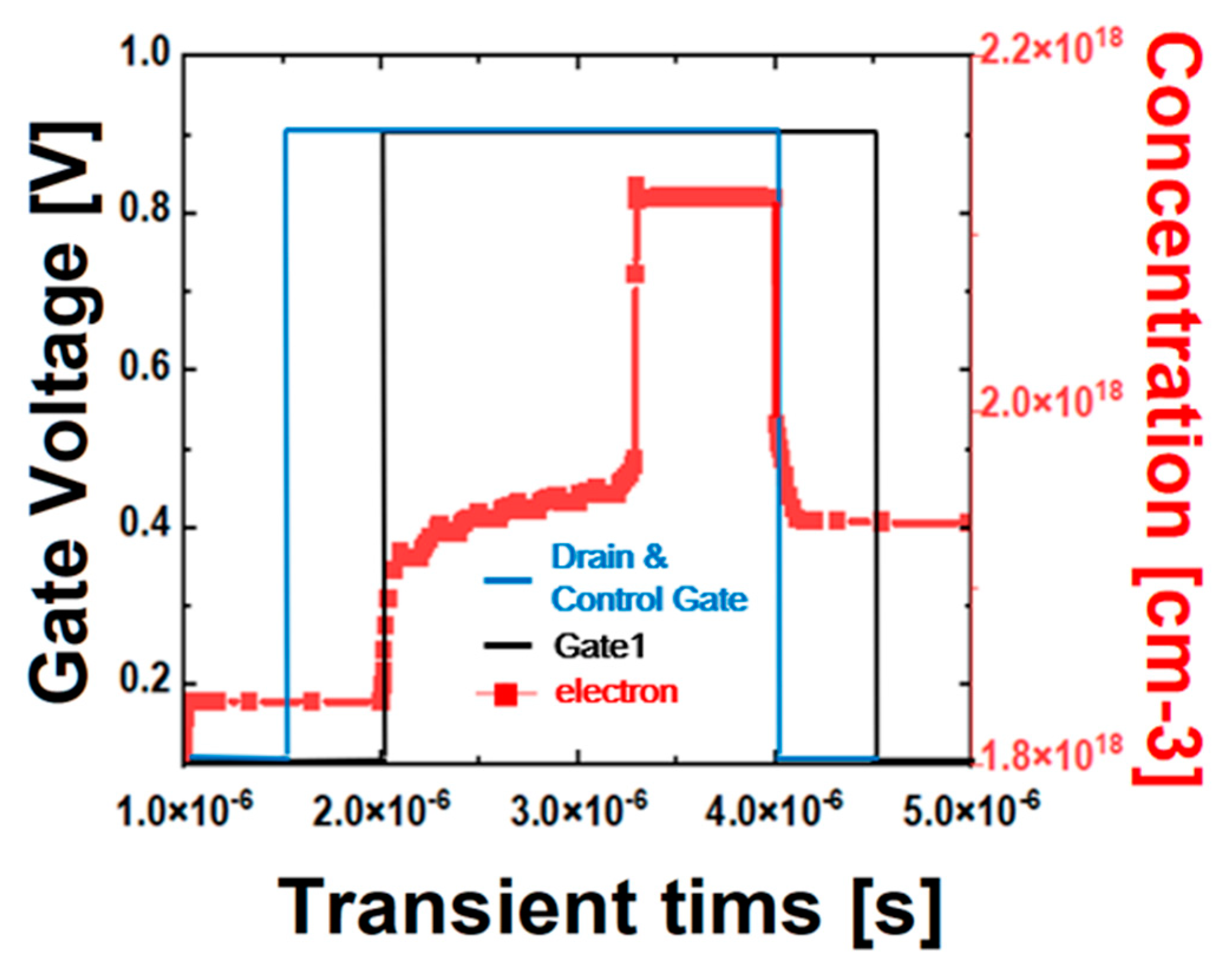
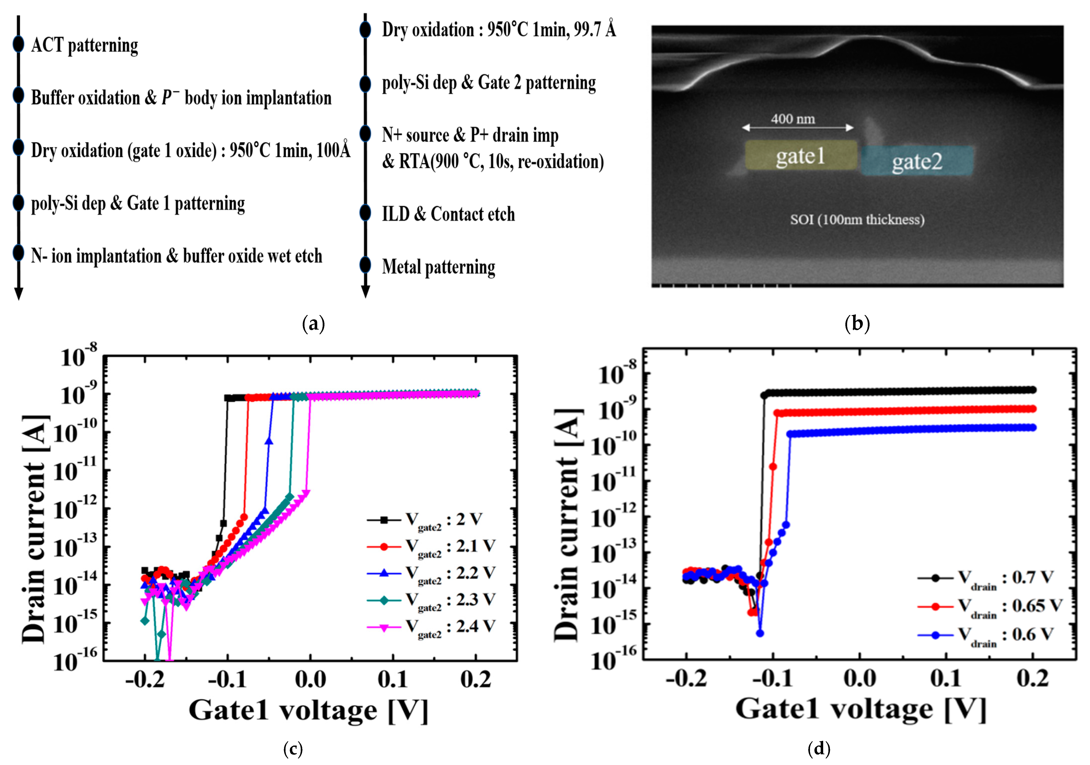
Consequently, the current is increased rapidly because of a positive feedback loop, and the FBFET is turned on. Figure 3 shows a difference in drain current according to various drain voltages. The drain current is constant after the FBFET is turned on, and it increases exponentially as Vd linearly increases. This is because the FEFET operates similarly to a forward-bias PN diode when the device is switched on by a positive feedback loop. When the gate voltage is equally applied, the drain v7oltage is applied from 0.8 V to 1.4 V, and FBFET has the highest current ratio when the drain voltage is the highest. Additionally, after the FBFET is turned on, the drain current is saturated. This is because after the FBFET is turned on, the current is determined only by the pn diode voltages (drain voltage and source voltage) and is not affected by the gate voltage. We confirm the excellent steep switching characteristics of the FBFET, and the subthreshold swing (SS) is 6.27 mV/dec when the drain voltage is 1.4 V. The FBFET also has a different potential well depth depending on the control gate voltage. As the control gate voltage increases, the depth of the potential well increases, and the threshold voltage increases. Likewise, as the control gate voltage decreases, the threshold voltage decreases. Figure 4a shows the energy band diagram. Figure 4b shows that as the control gate voltage increases, the turn-on time increases. If the potential well is deep, more electrons must be accumulated to turn on the device, so the turn-on time is longer. Figure 5 is a graph of the accumulation of electrons in the floating body over transient time. When an applied voltage is less than the threshold to gate 1, the electrons gradually accumulate in the floating body. Additionally, when the number of electrons exceeds the threshold, the FBFET is turned on by a feedback loop between the electrons and the potential barrier. The graph shows that it turns on and off very quickly. Therefore, we suppressed short circuit current using the steep switching characteristics of FBFET and replaced the role of a membrane capacitor using the characteristics of accumulating charge in the floating body. Figure 6 shows the process measurement of the proposed FBFET structure. Figure 6a shows the detailed fabrication process of the proposed FBFET. Since the manufacturing method is compatible with CMOS, FBFET has the advantage of being integrated with the CMOS circuit [19]. An SEM image of the fabricated device after gate patterning is shown in Figure 6b. In addition, we calibrated the simulation parameters based on the measurement results. (Figure 6c,d) [14]. These show the measurement result of the drain current that changes according to the various control gate voltages and the various drain voltages.

2.2. Multi-Gate FBFET for Multiple Inputs

Furthermore, we designed a multi-gate FBFET to implement neuronal network characteristics because neuron networks need to receive multiple signals from previous neurons. The proposed structure consists of four gates and one control gate. It is shown in Figure 7.
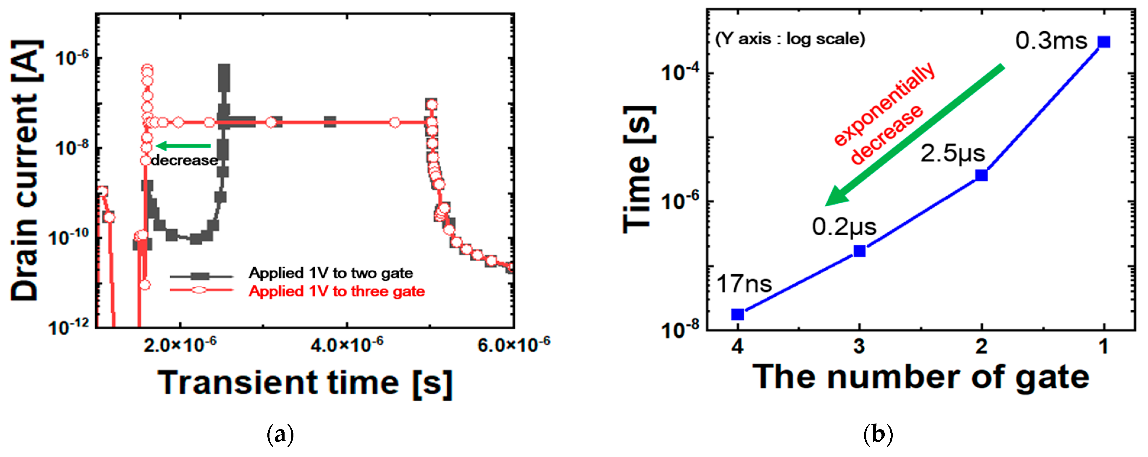
This structure can implement spatial integration by receiving multiple inputs through multi-gates. It also can store electric charges in the floating body, enabling temporal integration. Its simulation results are shown in Figure 8. We also used TCAD simulation for this. Figure 8a shows the turn-on time difference according to the number of gates applying voltage. Figure 8b shows the turn-on time of the FBFET according to the number of biased voltage gates. As the number of gates increases, the turn-on time exponentially decreases. Because as the number of applied gates increases linearly, the accumulated electrons in the potential well under the control gate also increase linearly. Additionally, as the number of electrons increases, the valence band height of the control gate decreases linearly. When the valence band height is linearly lowered, the accumulated holes increase exponentially. The associated energy band equation is as follows [20].
l h 0 = qA ( D p n p L p 1 + D n n p L p 1 ) ( e [ qV / kT ] 1 ) = l hi ( e [ ϕ e / kT ] 1 )
Due to this feedback, as the gates applied increase, the turn-on time decreases exponentially. Therefore, when multiple inputs are applied, it indicates that the charges are stored in the floating body, and the temporal integration is performed by the floating body.

3. Capacitor-Less Multiple Input Neuron Circuit

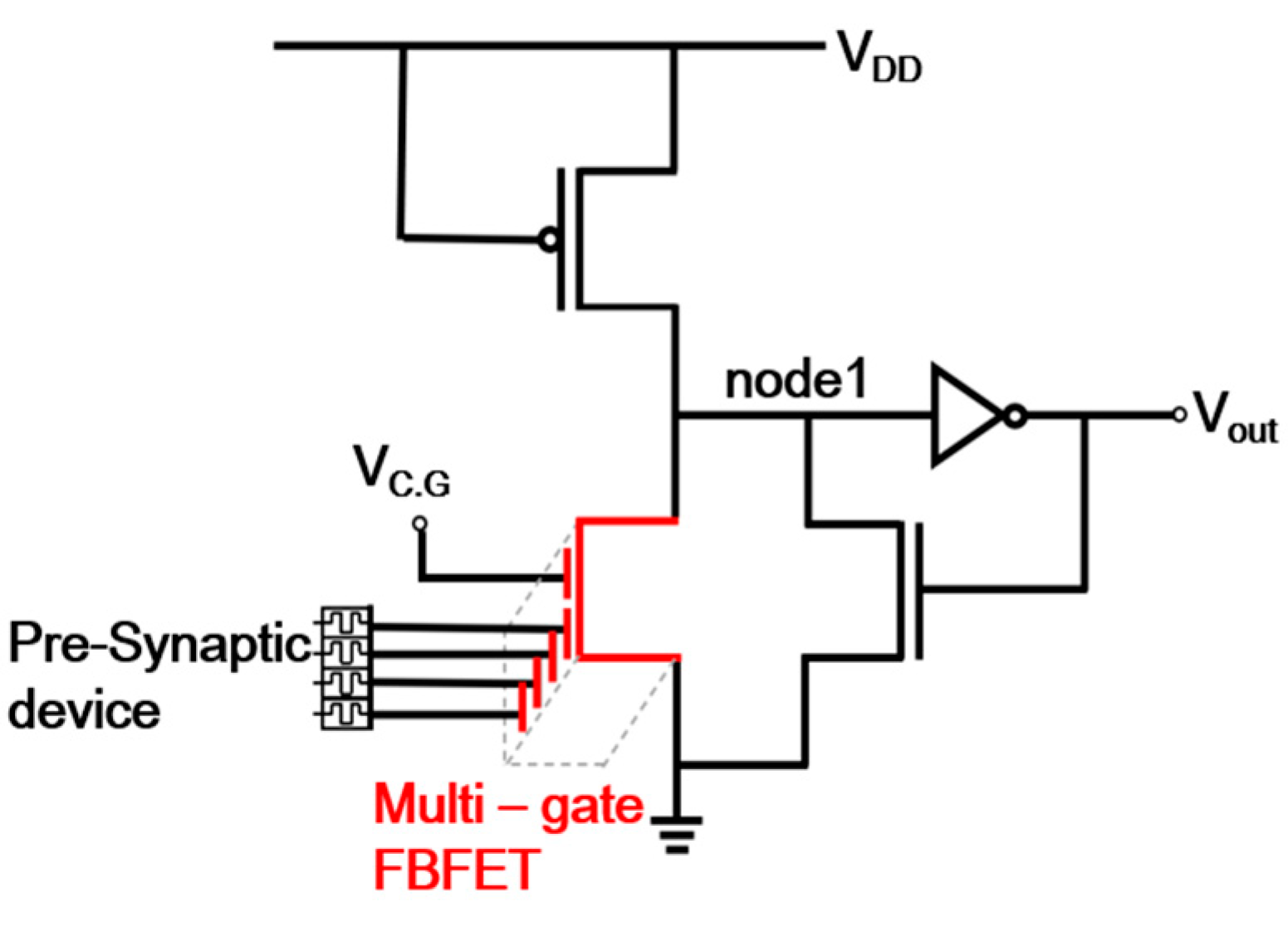
We designed a neuron circuit using multi-gate FBFET with previous simulation results. This circuit is illustrated in Figure 9. The multi-gate FBFET replaces a membrane capacitor, and it is used for the NMOS position. This neuron circuit completely inhibits leakage until a power spike occurs due to the steep switching characteristics of FBFET and low off-current. However, before the node1 voltage is discharged to the ground, the FBFET is quickly blocked as the drain voltage of the FBFET decreases. Consequently, the FBFET cannot lower the node1 voltage to the ground. To lower the node 1 voltage to the ground, we use N1 (NMOS1). First, the FBFET is turned on, and the node 1 voltage drops rapidly. As the node1 voltage drops, N1 is turned on by INV2, and the node1 voltage is discharged to the ground. Finally, the output spike has occurred, and the accumulated charge of the FBFET is removed by recombination. Additionally, since FBFET suppresses Isc during the accumulation period, node1 voltage is maintained.
Figure 10 shows the simulation results of the proposed neuron circuit. When the input voltage pulse is continuously applied at 1.1 V, electrons accumulate. When the threshold is exceeded, the number of electrons increases rapidly, and the first inverter output voltage (Vnode1) drops rapidly to 0. Additionally, analog neuron circuits generate short-circuit currents in which current flows before Vth, but the circuit only flows at the moment the FBFET is turned on. Through this, we confirmed that multi-gate FBFET could effectively replace a membrane capacitor, which can reduce area and energy consumption.

4. Conclusions

The existing von Neumann-based computing structure has great limitations in terms of power consumption and speed in terms of high-level information processing, and in order to implement deep learning that operates in real-time, many processors have problems related to area and power consumption. Neurons, known as nerve cells in the brain, recognize information through body sensory organs, send information to the brain, process it, and deliver commands to motor organs, and the human brain performs recognition, judgment, and learning at as low power as 20 W. To process a large amount of data, a neuromorphic architecture is essential, and a neuron circuit is required to implement a neuromorphic structure. Most of the neurons of the current neuromorphic chip are composed of analog and mixed-signal technology, and in the neural network, neurons generate spike signals when receiving stimulus signals, and each neuron exchanges signals and learns. However, analog neurons began to show limitations in terms of area and energy using operational amplifiers and capacitors. These problems are caused by the membrane capacitor, so we proposed a neuron circuit structure without the membrane capacitor. Additionally, according to the simulation results, a multi-gate FBFET can effectively receive multiple inputs and reduce the number of devices by replacing a membrane capacitor. Additionally, the neuron circuit using the device can solve the power consumption problem by suppressing the short-circuit current. We demonstrate through SILVACO TCAD simulations that a neuromorphic structure can be implemented using multi-gate FBFET. In other words, we suggest a new direction for neuromorphic architecture.

Author Contributions

Conceptualization: M.-W.K.; validation: J.L. and M.C.; investigation: J.L. and M.C.; writing—original draft preparation: J.L.; writing—review and editing: J.L. and M.-W.K.; visualization: J.L. and M.C.; funding acquisition: M.-W.K. All authors have read and agreed to the published version of the manuscript.

Funding

This work was supported by the National Research Foundation of Korea (NRF) grant funded by the Korean government (MSIT) (2021R1G1A1093786) and this research was supported by the National R&D Program through the National Research Foundation of Korea (NRF) funded by the Ministry of Science and ICT (NRF-2022M3I7A1078936).

Institutional Review Board Statement

Not applicable.

Informed Consent Statement

Not applicable.

Data Availability Statement

Not applicable.

Conflicts of Interest

The authors declare no conflict of interest.

References

  1. Sourikopoulos, I.; Hedayat, S.; Loyez, C.; Danneville, F.; Hoel, V.; Mercier, E.; Cappy, A. A 4-fJ/spike artificial neuron in 65 nm CMOS technology. Front. Neurosci. 2017, 11, 123. [Google Scholar] [CrossRef] [Green Version]
  2. Oliveira, J.F.; Araque, A. Astrocyte regulation of neural circuit activity and network states. Glia 2022, 70, 1455–1466. [Google Scholar] [CrossRef]
  3. Zhang, T.; Perkins, M.H.; Chang, H.; Han, W.; de Araujo, I.E. An inter-organ neural circuit for appetite suppression. Cell 2022, 185, 2478–2494. [Google Scholar] [CrossRef] [PubMed]
  4. Kwon, D.; Woo, S.Y.; Lee, J.H. Review of Analog Neuron Devices for Hardware-based Spiking Neural Networks. J. Semicond. Technol. Sci. 2022, 22, 115–131. [Google Scholar] [CrossRef]
  5. Rathi, N.; Agrawal, A.; Lee, C.; Kosta, A.K.; Roy, K. Exploring spike-based learning for neuromorphic computing: Prospects and perspectives. In 2021 Design, Automation & Test in Europe Conference & Exhibition (DATE); IEEE: Piscataway, NJ, USA, 2021. [Google Scholar]
  6. Saxena, V. Neuromorphic computing: From devices to integrated circuits. J. Vac. Sci. Technol. B Nanotechnol. Microelectron. Mater. Process. Meas. Phenom. 2021, 39, 010801. [Google Scholar] [CrossRef]
  7. Huynh, P.K.; Varshika, M.L.; Paul, A.; Isik, M.; Balaji, A.; Das, A. Implementing spiking neural networks on neuromorphic architectures: A review. arXiv 2020, arXiv:2202.08897. [Google Scholar]
  8. Yamazaki, K.; Vo-Ho, V.K.; Bulsara, D.; Le, N. Spiking neural networks and their applications: A Review. Brain Sci. 2022, 12, 863. [Google Scholar] [CrossRef]
  9. Dora, S.; Kasabov, N. Spiking neural networks for computational intelligence: An overview. Big Data Cogn. Comput. 2021, 5, 67. [Google Scholar] [CrossRef]
  10. Poon, C.-S.; Zhou, K. Neuromorphic silicon neurons and large-scale neural networks: Challenges and opportunities. Front. Neurosci. 2011, 5, 108. [Google Scholar] [CrossRef] [PubMed] [Green Version]
  11. Indiveri, G.; Chicca, E.; Douglas, R. A VLSI array of low-power spiking neurons and bistable synapses with spike-timing dependent plasticity. IEEE Trans. Neural Netw. 2006, 17, 211–221. [Google Scholar] [CrossRef] [PubMed] [Green Version]
  12. Park, Y.S.; Woo, S.; Lim, D.; Cho, K.; Kim, S. Integrate-and-fire neuron circuit without external bias voltages. Front. Neurosci. 2021, 15, 644604. [Google Scholar] [CrossRef] [PubMed]
  13. Sung, J.; Shin, C. Understanding of carriers’ kinetic energy in steep-slope P+ N+ P+ N+ feedback field effect transistor. Semicond. Sci. Technol. 2022, 37, 105014. [Google Scholar] [CrossRef]
  14. Kwon, M.W.; Baek, M.H.; Hwang, S.; Park, K.; Jang, T.; Kim, T.; Lee, J.; Cho, S.; Park, B.G. Integrate-and-fire neuron circuit using positive feedback field effect transistor for low power operation. J. Appl. Phys. 2018, 124, 152107. [Google Scholar] [CrossRef]
  15. Oh, J.H.; Yu, Y.S. Macro-Modeling for N-Type Feedback Field-Effect Transistor for Circuit Simulation. Micromachines 2021, 12, 1174. [Google Scholar] [CrossRef] [PubMed]
  16. Kim, M.; Lee, K.; Kim, S. A review of feedback field-effect transistors: Operation mechanism and their applications. J. IKEEE 2018, 22, 499–505. [Google Scholar]
  17. Lee, C.; Shin, C. Study on Various Device Structures for Steep-Switching Silicon-on-Insulator Feedback Field-Effect Transistors. IEEE Trans. Electron Devices 2020, 67, 1852–1858. [Google Scholar] [CrossRef]
  18. Kim, M.; Kim, Y.; Lim, D.; Woo, S.; Cho, K.; Kim, S. Steep switching characteristics of single-gated feedback field-effect transistors. Nanotechnology 2017, 28, 055205. [Google Scholar] [CrossRef]
  19. Lee, I.; Park, H.; Nguyen, Q.T.; Kim, G.; Cho, S.; Cho, I. Optimization of Feedback FET with Asymmetric Source Drain Doping profile. Micromachines 2022, 13, 508. [Google Scholar] [CrossRef] [PubMed]
  20. Lee, C.; Sung, J.; Shin, C. Understanding of feedback field-effect transistor and its applications. Appl. Sci. 2020, 10, 3070. [Google Scholar] [CrossRef]
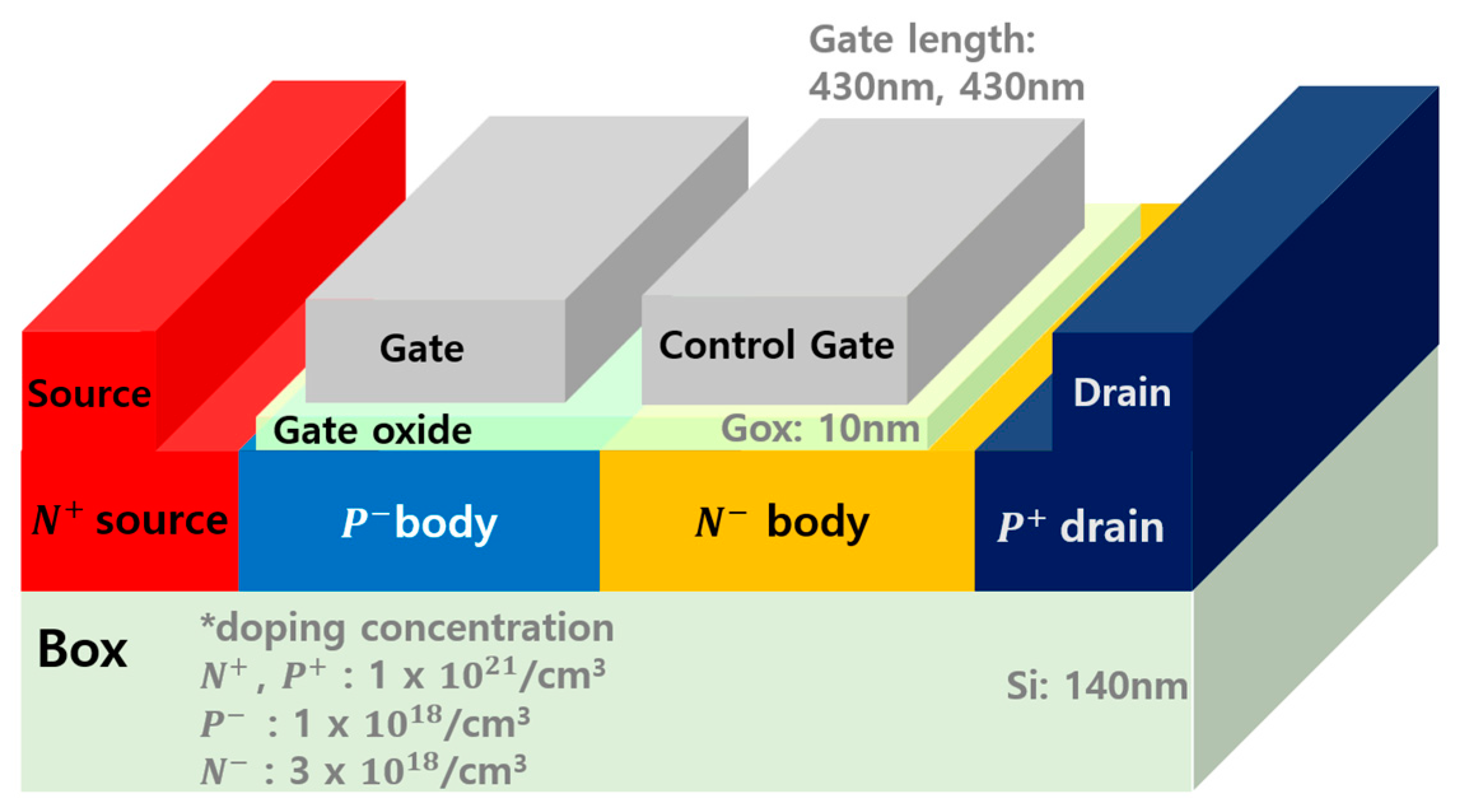
Figure 1. Simulation FBFET Structure with parameters.
Applsci 13 02628 g001
Figure 2. Energy band diagram of the FBFET when it turned on.
Applsci 13 02628 g002
Figure 3. Transfer characteristics for various drain voltages from 0.8 V to 1.4 V. The higher the applied drain voltage, the higher the drain current. (Control gate V = 2 V).
Applsci 13 02628 g003
Figure 4. Characteristics according to control gate voltage. (a) Energy band diagram of the FBFET. As increasing Control gate bias, potential well is deeper. (b) Transfer curve for various control gate voltage. As the control gate voltage increases, the turn-on time increases.
Applsci 13 02628 g004
Figure 5. Transient simulation result of accumulated electrons concentration. The electrons accumulate gradually and fbfet is turned on by a feedback loop when the number of electrons exceeds the threshold. ( V D S = V C . G = V G 1 = 0.9   V ).
Applsci 13 02628 g005
Figure 6. Multi-gate FBFET simulation result. (a) Compared on/off time between two and three gates that applied voltage (b) Graph of turn-on time according to the number of gates applied with a voltage. The time decreases exponentially as the number of gates increases (Control gate V = 0.9 V) (c) Id-vg curve measurement result according to control gate voltage (Vgate2 = Vcontrol gate) (d) Transfer curve measurement result according to drain bias.
Applsci 13 02628 g006
Figure 7. Proposed multi-gate FBFET structure.
Applsci 13 02628 g007
Figure 8. Multi-gate FBFET simulation result. (a) Compared on/off time between two and three gates that applied voltage (b) Graph of turn-on time according to the number of gates applied with a voltage. The time decreases exponentially as the number of gates increases (Control gate V = 0.9 V).
Applsci 13 02628 g008
Figure 9. Proposed neuron circuit diagram with Multi-gate FBFET.
Applsci 13 02628 g009
Figure 10. The neuron circuit with multi-gate FBFET simulation result. (a) Simulation results of single and two gates that applied voltage electron accumulation (b) Steep drain current graph of proposed neuron circuits with no leakage current during the Vin pulses. (Control Gate V = 1.1 V).
Applsci 13 02628 g010
Disclaimer/Publisher’s Note: The statements, opinions and data contained in all publications are solely those of the individual author(s) and contributor(s) and not of MDPI and/or the editor(s). MDPI and/or the editor(s) disclaim responsibility for any injury to people or property resulting from any ideas, methods, instructions or products referred to in the content.