Article

Reactive Ion Etching of X-Cut LiNbO3 in an ICP/TCP System for the Fabrication of an Optical Ridge Waveguide

1
Faculty of Physics, Perm State University, 15 Bukireva str., 614068 Perm, Russia
2
Department of General Physics, Perm National Research Polytechnic University, 614990 Perm, Russia
3
Center for Photonics and 2D Materials, Moscow Institute of Physics and Technology, 9 Institutskiy per., 141701 Dolgoprudny, Russia
4
Institute of High Technologies and Advanced Materials, Far Eastern Federal University, 690922 Vladivostok, Russia
*
Author to whom correspondence should be addressed.
Appl. Sci. 2023, 13(4), 2097; https://doi.org/10.3390/app13042097
Submission received: 24 December 2022 / Revised: 31 January 2023 / Accepted: 3 February 2023 / Published: 6 February 2023
(This article belongs to the Special Issue Advances and Application of Lithium Niobate)

Abstract

:
In this study, the technology for producing ridge waveguides with a minimal roughness of the sidewalls and material surface in a near-waveguide region was developed with the purpose of fabricating miniature photonic integrated circuits on a LiNbO3 substrate. Plasma etching processes were used for the ridge waveguide fabrication on different material substrates. The specifications of the equipment and plasma source, method of mask fabrication and substrate material determined the process conditions for producing ridge waveguides with minimal sidewall roughness. In this work, for the ridge waveguide fabrication, the processes of reactive ion etching of LiNbO3 with a chromium mask were carried out in a mixture of SF6/Ar with an ICP/TCP plasma source. The process of plasma etching the LiNbO3 with the ICP/TCP plasma source is not well studied, especially for integrated photonics purposes. As a result of our experimental work, the narrow ranges of technological parameters suitable for producing ridge waveguides on LiNbO3 with smooth sidewalls, a slope angle of 60°–75° and a minimal quantity of observed defects in the near-waveguide region were identified. A model explaining the kinetics of the etching process of LiNbO3 in SF6/Ar plasma as a physical–chemical process was proposed.

1. Introduction

Lithium niobate on insulator (LNOI) or thin-film lithium niobate is a promising substrate for the production of high-frequency (up to 1 THz and more [1]) miniature photonic integrated circuits (PICs). The formation of two European platforms based on the application of LNOIs for PICs was started in 2022 (LOLIPOP (in combination with silicon-nitride (TriPleX) technology) [2] and ELENA [3]). This fact and the increasing number of science publications (for example [4,5]) demonstrate the growing interest in LNOI for integrated optics applications around the world over the past few years.
Using LNOI makes it possible to form high-contrast optical waveguides with a comparatively small curvature radius (100 μm or less) and, consequentially, fabricate PICs with a high integration density (50–100 basic elements on less than 1 cm2). In the field of radio frequency (RF) applications, the use of LNOI provides an opportunity to adjust the propagation velocity of RF electric and optical waves and, as a result, to build miniature RF modulators [6] and high-frequency PICs based on it.
Currently, the authors of this paper are focusing on developing the technology of PIC fabrication on LNOI substrates. The main basic step in this process is the search for technological regimes for producing waveguides with a minimal roughness of the sidewalls and material surface in the near-waveguide region.
Typically, when producing integrated optical waveguides, a dry plasma etching process is used. In this case, significant efforts are being made to obtain the technological regimes for producing optical waveguides by multiple research groups applying a wide range of plasma sources and plasma-forming gases. As a consequence, the variety of regimes presenting a different quality and morphology of resulting surfaces were revealed (Table 1).
In this study, the “quality” was measured using the following characteristics: the slope angle of optical waveguide sidewalls, aspect ratio, roughness of the sidewalls and material surface in the near-waveguide region. These characteristics significantly affect the light propagation in a waveguide and the waveguide parameters (such as backscattering, radiation losses and polarization maintenance).
As shown in Table 1, ICP and ICP/RIE are the most commonly used types of plasma sources for the dry etching of LiNbO3 (LN), and the majority of processes were carried out in a mixture of fluorine-containing gases and argon. Such a gas mixture makes it possible to form a profile of an optical waveguide with nearly vertical sidewalls [7,10,11,12,13,14], but the formed structures have a high surface roughness [7,8,10,14,16]. Relatively high-quality structures were obtained in [9], but Z-cut LiNbO3 was used as a substrate (Z-cut has a diverse X-cut etching mechanism that is complicated to use for RF PICs fabrication on LNOI since driving electrodes should be located above and below the optical waveguide).
LiNbO3 is well-known for being difficult to dry etch [17]. To overcome this in studies [11,12,13,15], proton-exchanged (PE) LiNbO3 was exposed to plasma. After the PE process, the concentration of Li ions in the near-surface layer of LiNbO3 decreases, which subsequently has a positive effect on the roughness and aspect ratio of the plasma-etched surface and microstructures.
At another point, the PE process of LiNbO3 leads to the formation of a near-surface layer with structural disorder and the degradation of electro-optical and nonlinear properties of materials [18,19] that adversely impact the performance parameters of basic integrated optical building blocks and PICs.
The aim of this research was to determine the process parameters of reactive ion etching of initial (without a near-surface PE layer) LiNbO3 in a mixture of SF6/Ar gases for developing the technological process of forming integrated optical waveguides with the required aspect ratio and minimal roughness of sidewalls and material surface in the near-waveguide region.
Dry plasma etching of LiNbO3 is quite a challenge. The process is complicated by the formation of the non-volatile compound LiF on the substrate surface during the treatment in fluorine-containing plasma. The formation of LiF on the surface results in a significant decrease in the etching rate, a reduction in the aspect ratio of microstructures and an increase in the surface roughness [20].
Nagata H. et al. [21,22] demonstrated that the structure of LiF that forms during the process depends on plasma-forming gas mixture: it has an amorphous structure in CHF3 plasma and is crystalline in CF4 plasma.
Some of the researchers consider the formation of LiF on the surface of LiNbO3 as a redeposition process without explaining its kinetics [7,13,14].
In [23], as well as in several related papers, Gulyaev V. et al. presented an experimentally confirmed model that explains the kinetics of the etching process of LiNbO3 in a fluorine-containing plasma. This model was based on the concept of topochemical reactions and describes the stages of LiF-film formation in the case of radical etching of LiNbO3 with a dominating chemical plasma component.
Our group proposed the extension of Gulyaev’s model [23] to the reactive ion etching (RIE) process, where accelerated ions bombard the substrate surface, and the physical component of the plasma becomes significant and cannot be excluded from consideration. It should be taken into account in order to expand the model explaining the kinetics of LiNbO3 etching in SF6/Ar plasma as a physical–chemical process.
The results of a large number of experiments were considered and discussed in the terms of the proposed extended model. The narrow ranges of technological parameters suitable for producing the ridge waveguides on LiNbO3 with smooth sidewalls, a slope angle of 62°–75° and a minimal quantity of observed defects in the near-waveguide region were identified.

2. Materials and Methods

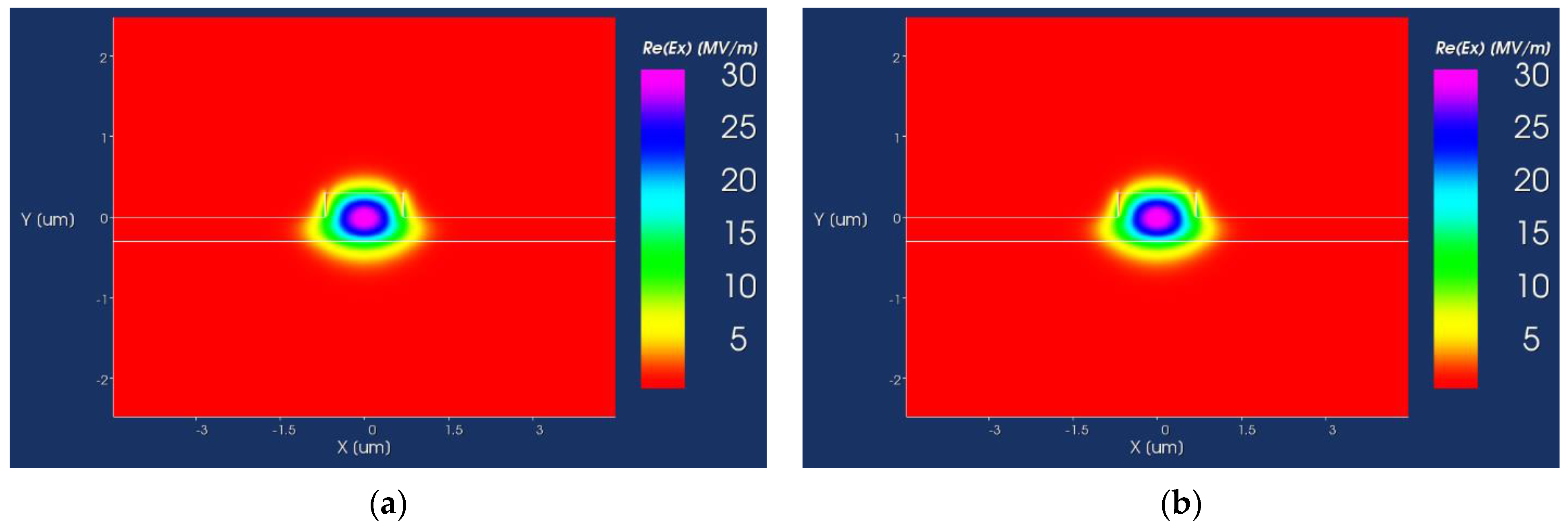
2.1. Numerical Simulations for Developing the Topology of Optical Waveguides on an LNOI Substrate

The numerical simulation of an optical waveguide needs to be done to determine the typical sizes of basic and some test microstructures, etching depth, aspect ratio of structures, admissible slope angle, and other specifications of the technological process and the final result (the cross-section of the fabricated waveguide). Furthermore, the designs of an optical waveguide topology and all basic building blocks are based on the results of numerical simulation. In this study, the developed design (topology of optical waveguides) was used to fabricate a photolithographic mask.
To design the topology, numerical simulation with the finite-difference frequency domain (FDFD) method was carried out. The main goal of the simulation process was an optimal waveguide parameters evaluation. The waveguide cross-section geometry for single-mode light propagation was optimized, and the critical bending radii were calculated.
The simulation was carried out by taking into account the configuration of the LNOI wafers produced by NanoLN (China): the thickness of the SiO2 layer was 4.7 µm and the thickness of the LiNbO3 layer was 0.6 µm.
Two types of integrated optical waveguides can be implemented on LNOI: deep-etched and shallow-etched waveguides.
On the one hand, according to published articles, shallow-etched optical waveguides are characterized by smaller scattering losses induced by sidewall roughness in comparison with deep-etched waveguides [24,25,26,27,28].
On the other hand, deep-etched optical waveguides are characterized by smaller critical bending radii in contrast to shallow-etched ones [24,25,27]. This opportunity is crucial in cases with a high element integration density.
In order to reveal the single-mode condition of light propagation in waveguides, the etch depth and waveguide width were varied. In subsequent calculations, we used the parameters of the waveguide cross-section that are close to high-order mode excitation. Normally, waveguides with a large cross-section provide higher optical mode confinement and, therefore, lower scattering losses induced by sidewall roughness.
The following parameters of the calculation window were used: calculation window width—9 μm, calculation window height—5 μm, discretization density—251 points per axis and a perfectly matched layer was used as a boundary condition.
The dispersion in the medium was determined with the Sellmeier equations:
n S i O 2 ( λ ) = 1 + 0.6961663 λ 2 λ 2 0.0684043 2 + 0.4079426 λ 2 λ 2 0.1162414 2 + 0.8974794 λ 2 λ 2 9.896161 2 ,
n L i N b O 3 o ( λ ) = 1 + 2.6734 λ 2 λ 2 0.01764 2 + 1.2290 λ 2 λ 2 0.05914 2 + 12.614 λ 2 λ 2 474.60 2 ,
where λ is the wavelength of light (typically, 1550 nm) [29,30].
As a result, the optimal cross-section parameters were defined: waveguide width—1.4 μm and etching depth—0.3 μm (in the case when the cladding refractive index was equal to 1). This configuration of the waveguide supports the single-mode condition of light propagation with wavelengths in the range of 1.5 μm to 1.6 μm. In addition, the calculated critical bent radius was 50 μm with bend optical losses less than 0.001 dB/90°. Figure 1 shows the results of the numerical simulation: the distribution of the E-field in the cross-sections of both the straight and bent waveguides is presented.
Based on the results of the numerical simulation, the photolithographic mask containing the design of the optical waveguides topology was fabricated.

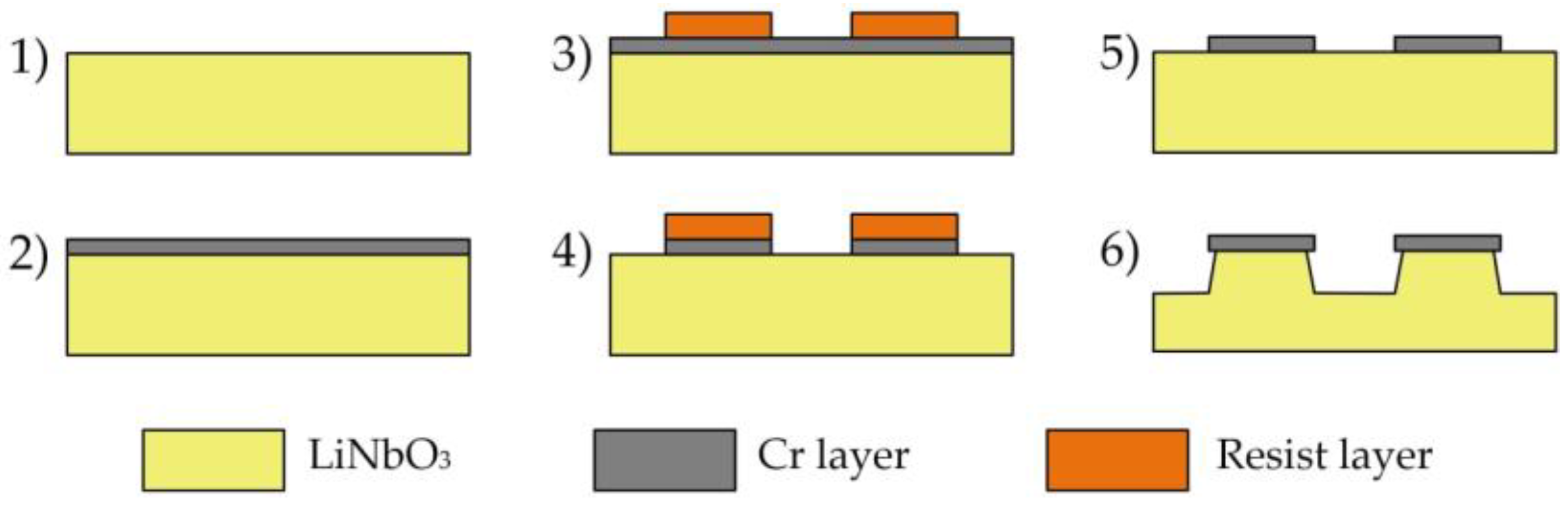
2.2. Sample Preparation

In this study, the bulk X-cut LN (produced by CQT, China) was used as a substrate for developing appropriate process regimes of plasma etching because of the expensiveness of LNOI substrates. In the future, the obtained process regimes will be transferred to X-cut LNOI for producing basic integrated optical building blocks.
The sample preparation in this research consisted of the following stages: substrate cleaning and the formation of a hard mask. The stages are schematically shown in Figure 2 and their descriptions are given below.
First, the cleaning procedure of LN wafers was carried out in Piranha solution (H2SO4:H2O2 = 3:1; 5 min cleaning time) followed by isopropyl alcohol with an intermediate rinsing of substrate in deionized (DI) water and blowing with dry N2 [31].
After LN cleaning, the 80 nm-thick chromium layer was deposited on the substrate surface (Figure 2, stage 2). The deposition process was carried out with DC magnetron sputtering using the following conditions: the applied DC magnetron power was 500 W, the Ar flow was set equal to 0.7 L/h and the substrate temperature was 200 °C.
To eliminate the residual stress in the chromium thin film, the samples after deposition were annealed at 300 °C over 1 h in a dry nitrogen atmosphere (with N2 flow at 2 L/h). The residual stress in the chromium film (as the hard mask) may be able to affect the undercut (an unwanted side effect) during the following etching process. The abovementioned conditions of magnetron sputtering and thermal annealing were obtained during a huge set of experiments and verified with published data.
At the stage of the etching technology transfer from bulk LN to LNOI wafers, it is important to pay attention to the additional stress in the stack of thin films, which occurs during the annealing step (because of different thermal expansion coefficients of the materials). In order to minimize the risk of defect formation in the LNOI waveguide films, it is important to follow the instructions for the thermal treatment of LNOI wafers provided by the NanoLN vendor. The heating/cooling rate should be kept at ~3 °C/min in all thermal steps of the process.
In the next stage, the samples were coated with a 500 nm-thick negative resist layer AZnLOF 2020 diluted with PGMA. The pattern of the variety of test structures and topology of the optical waveguides were formed in a resist layer with contact lithography (Figure 2, stage 3). The design of the topology was developed based on numerical simulation of the optical waveguides on an LNOI substrate. A detailed description is provided above.
It was revealed during the set of experiments that hard-baking the resist improved the repeatability of the following process of etching the chromium layer. This is why after the resist development, it was hard-baked on a hot plate according to the technical datasheet at 150 °C over 1 min.
After the lithography stage, the chromium layer was etched in a solution of cerium ammonium nitrate (CAN) (50 g CAN powder compound, 10 mL of acetic acid and 500 mL of DI water), which has good selectivity for AZ nLOF 2020 and other used materials (Figure 2, stage 4). The etching was carried out at 50 °C over 1.5 min with constant stirring.
The mask profile after the etching of the chromium layer was investigated with a scanning electron microscope (SEM) Tescan Mira. The SEM image of the cross-section of the LN sample after this stage is shown in Figure 3a. At the final stage, the resist was removed in dimethyl sulfoxide solvent at 80 °C; the top view of the Cr strip after removing the resist layer is shown in Figure 3b. The width of the obtained structures in the chromium layer decreased by 10% of the width of the designed structures in the photolithographic mask due to under-etching.
The quality of the Cr mask was evaluated using the line edge roughness (LER) parameter. The LER measurement was carried out as follows: SEM images of several Cr strips (hard mask for the waveguide structures) were obtained at the same magnification (100 k), and then the LER parameter was estimated using image processing in the specially developed Python program. An average value of the LER parameter characterizing the quality of the Cr mask ranged from 20 to 30 nm.
The LiNbO3 wafers with the formed chromium hard mask were cut into 2 × 2 cm2-sized samples with a saw dicing Disco DAD 320, then the reactive ion etching process was carried out using an inductively coupled plasma (ICP-RIE) system Ethna-100.

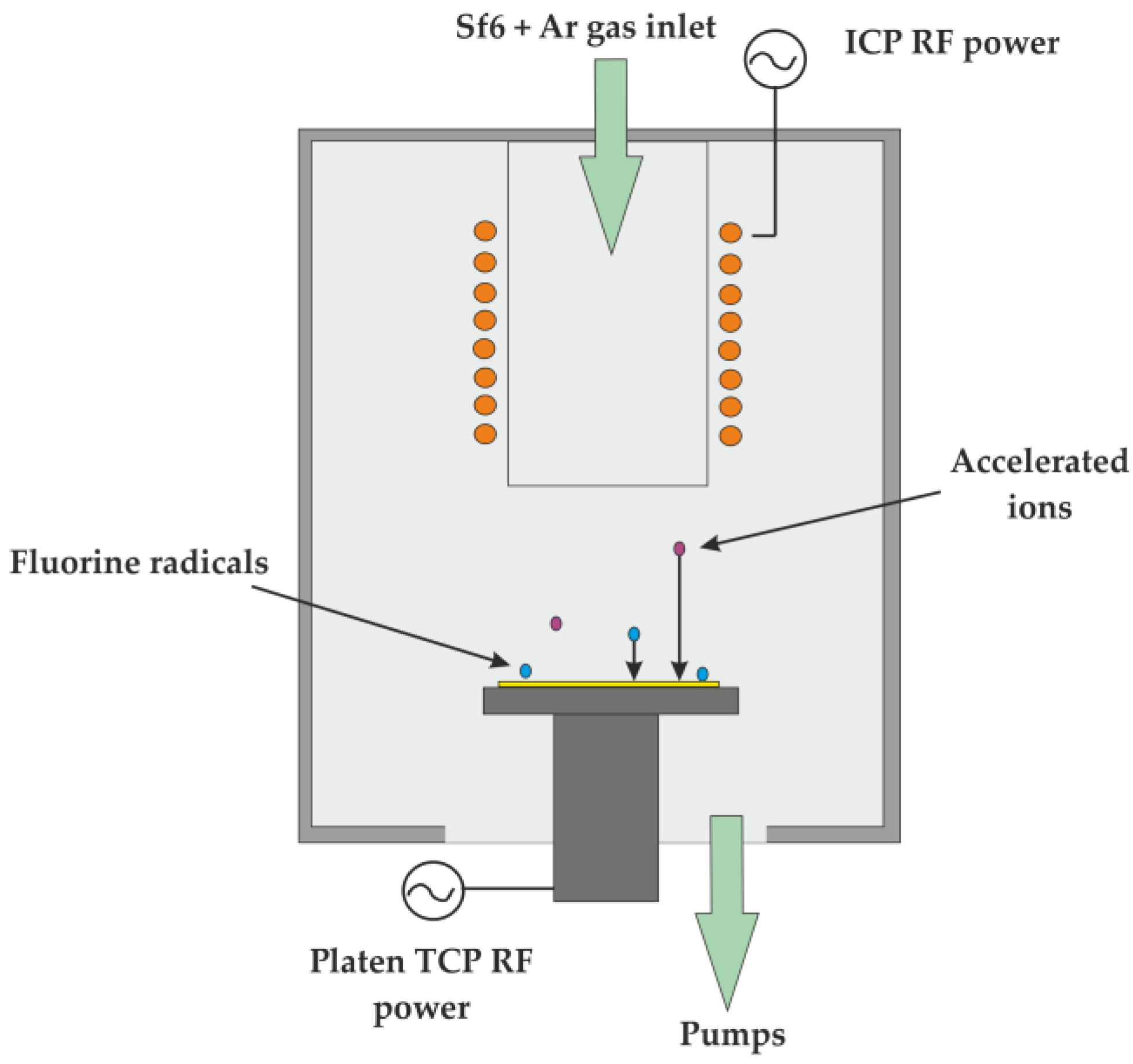
2.3. Reactive Ion Etching

The schematic representation of the ICP-RIE system Ethna-100 is shown in Figure 4.
The etching process was carried out in a mixture of SF6 and Ar gases. The base pressure in the equipment was 3 × 10 4 mbar. The substrate stage was water-cooled and the temperature in the cooling circuit was 20 °C.
The settings of the Ethna-100 system provides the opportunity to control the ion flux and ion kinetic energy independently of each other by changing the power on the ICP and TCP sources, respectively. The system allows for setting the ICP power up to 600 W and the TCP power up to 300 W. Gas flows may be varied in the range from 0 to 70 sccm.
Based on the research results that were found in the articles presented in Table 1, the ranges of the process parameters were reduced to the following values: ICP power—300–600 W, TCP power—50–200 W, process pressure—0.007–0.8 mbar and etching time—8 min. The influences of various ratios of SF6 and Ar were also investigated.
After the plasma etching process, chromium was removed using a selective etchant.
To control the quality of the obtained profile of the waveguides, a transverse cleavage of the samples was carried out, then cleaved samples were studied with an SEM. Numerical measurement of the roughness with atomic force microscopy was not carried out. The resolution of the SEM images made it possible to qualitatively evaluate the surface roughness. The LER parameter of the waveguides was also calculated using the SEM images. Energy-dispersive X-ray spectroscopy (EDX) was used for a qualitative assessment of the presence of elements on the surface.

3. Results

As a result of the set of experiments, technological regimes for producing waveguides with better surface and profile qualities were determined and are summarized in Table 2. We note that the work is ongoing and further minor adjustments to the finally selected technological regime are possible. The development of the RIE etching process was done in two iterations: first, modes similar to those published in the articles (Table 1) were tested. Recipe #13 provided the most acceptable profile quality in the first iteration. Second, recipes #14–#17 were tried in an attempt to improve the quality of the results that recipe #13 gave and, finally, recipes #14–#17 showed improved structure anisotropy.
The etching depths for the given recipes varied from 0.23 to 0.60 μm, the mask selectivity varied from 1:4 to 1:8 and the best value of the slope angle of the waveguide sidewall obtained in this work was 70–75° (depending on the recipe).
A detailed description of the waveguide profiles formed with various etching recipes is presented below. The SEM images of two formed waveguides are shown in Figure 5.
An SEM image of the waveguide profile etched with recipe #13 is shown in Figure 5a.
The sidewall angle of the waveguide formed with recipe #13 was ~62° and the surface in the near-waveguide region was smooth. The LER value of the formed waveguide after RIE etching was equal to the LER value of the hard mask because the sidewall roughness of the waveguide was inherited from the hard mask.
The SEM image of the waveguide profile etched with recipe #14 is shown in Figure 5b, where the slope angle of the waveguide sidewalls was ~75°.
Despite the predictable improvement in the etching anisotropy (increasing the slope angle of the waveguide side wall) associated with decreasing the process pressure during the etching with recipe #14 in comparison to the process with recipe #13, the surface roughness in the near-waveguide region increased drastically after etching with recipe #14.

4. Discussion

A detailed comparison of the surface state of the samples etched with recipes #13 and #14 was undertaken for an analysis of the obtained results and an understanding of the kinetics of the etching process. Magnified views of the samples’ surfaces etched with recipes #13 and #14 are shown in Figure 6.
The following should be noted:
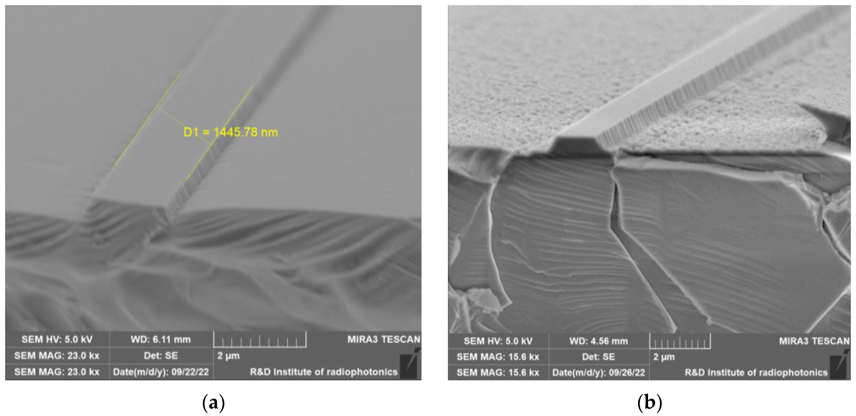
  • The mask selectivity was equal to 1:5.3 during the etching with recipe #13, and after the reduction in the pressure during the etching with recipe #14, the mask selectivity improved to 1:8.
  • The surface roughness in the near-waveguide region dramatically increased when recipe #14 was used.
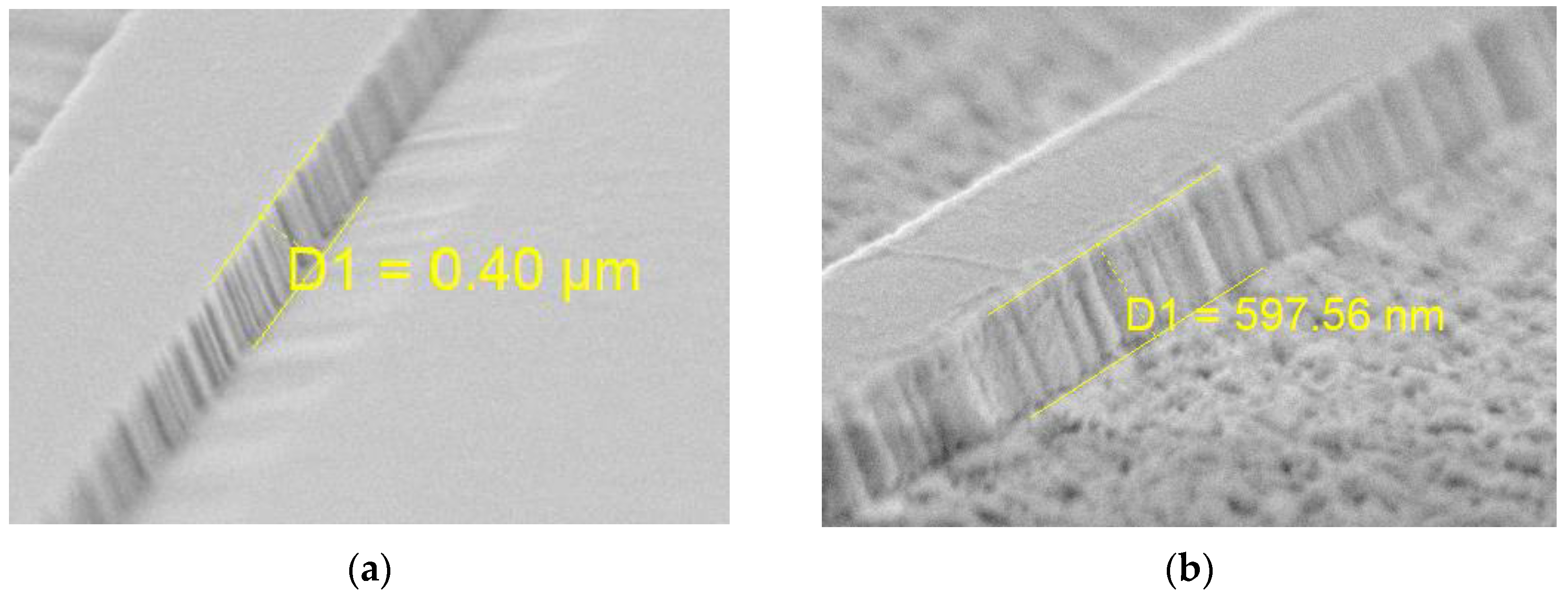
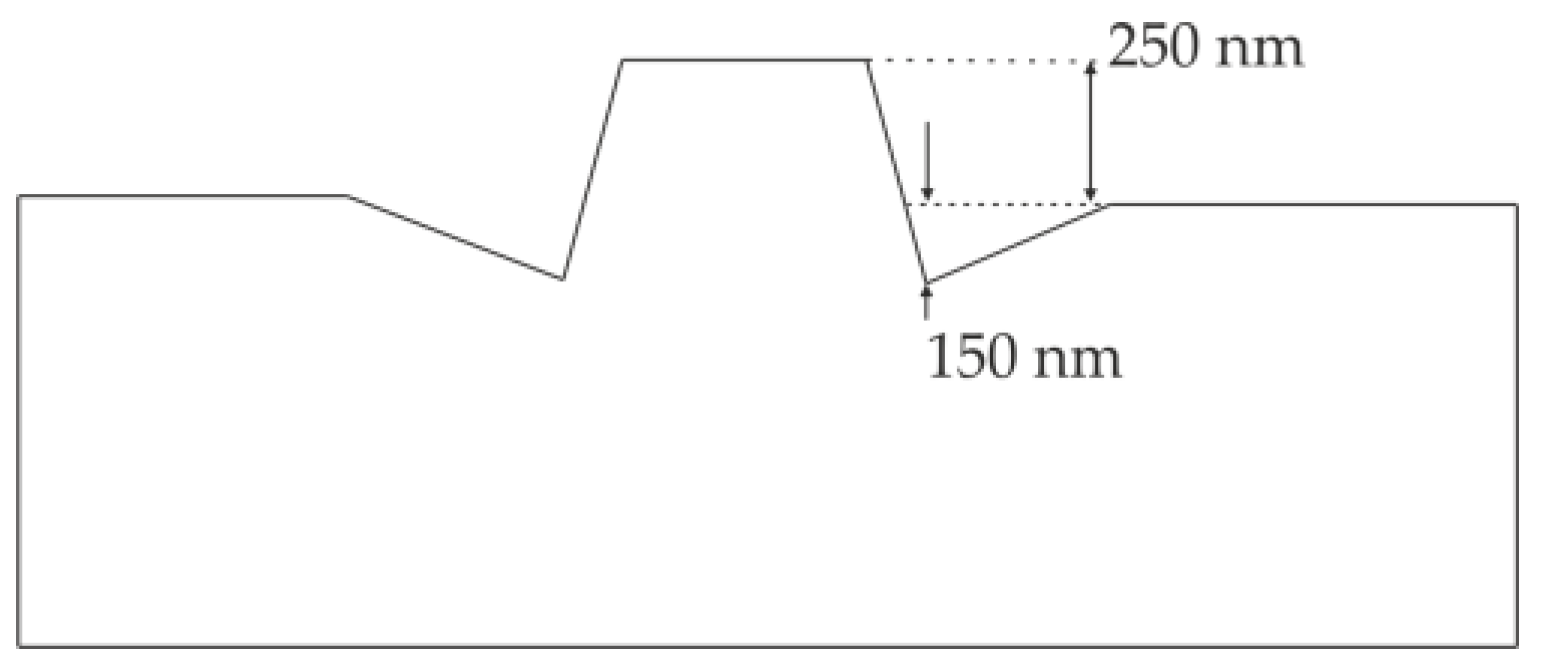
  • During the etching with recipe #13, microtrenches were formed along the waveguide base. A schematic representation of the waveguide profile obtained with recipe #13 is shown in Figure 7.
Microtrenches may affect optical mode characteristics, such as the confinement factor; however, a detailed analysis was not performed during this work.
It is shown in articles [32,33,34] that the microtrench formation process is a feature of RIE processes, where the physical component of the plasma has a significant impact. According to mentioned articles, the reason for the microtrench formation is as follows. Positive ions are accelerated to the wafer by the RF-biased electrode sheath. At the same time, plasma electrons tend to accumulate on the sidewalls of the feature (i.e., edges of the mask layer and any microstructures with relief, including the waveguide sidewalls). Therefore, ion trajectories tend to be deflected toward sidewalls, resulting in increasing the etching rate near the edges of the feature (including the base of the waveguide) and reducing the etching rate over a distance from features. In the case of a low etching pressure (<10 Pa or 0.1 mbar) and a relatively high biasing potential, the physical component of plasma, namely, accelerated ions, becomes significant and, as a consequence, microtrenches may be formed, which happened during the etching with recipe #13. During the RIE process with recipe #14, microtrenches were not formed.
Regarding mask selectivity, chromium was not chemically etched in the used gas mixture, and the decrease in mask selectivity during the RIE with recipe #13 also indicated an increased influence of the physical component of the plasma.
Let us consider the kinetics model of the LiNbO3 etching process proposed by Gulyaev V. et al. in [23] to explain the results obtained in this work after the RIE with recipe #14.
Gulyaev V. et al. considered the radical etching process of LiNbO3 as a topochemical reaction. The proposed model was based on experimental data for a range of pressures from 10 to 1000 Pa. In the case of an absence of a significant bias voltage, the abovementioned pressure range determines the etching mode with a dominating chemical plasma component, where the energy of the physical plasma component is insufficient for the near-surface layer sputtering and defects creation.
The authors [23] explained the kinetics of plasma etching as a two-stage process that includes the induction period and the stage of intense etching.
The etching rate is low during the induction stage. This stage includes the following:
  • Diffusion of the fluorine radicals from the plasma to the sample surface via a plasma sheath.
  • Adsorption of fluorine radicals on the surface of the LiNbO3.
  • Diffusion of adsorbed atoms into the near-surface layer.
  • The chemical reaction of fluorine with Li, Nb and O atoms and the formation of volatile fluorides and oxyfluorides (NbF5, NbOF3, OF2) and non-volatile LiF.
  • Swelling of the near-surface layer due to the accumulation of volatile compounds [23].
Fluorine easily diffuses into the structure of LiNbO3 because of the small positive ion radius (atomic radius of fluorine = 65 pm [35]); however, the out-diffusion of the reaction products is obstructed.
At the stage of intense etching, a drastic increase in the etching rate occurs as a result of the rupture of the cavity with the reaction products, and a polycrystalline LiF film with a porous structure forms on the surface.
Based on the model described above, the received results may indicate that plasma–chemical etching with a dominant chemical component of plasma occurred during process #14 rather than during the RIE process.
The sample surface was covered with a brown film-like layer after the etching process with recipe #14. The SEM-EDX analysis of the near-surface layer was carried out using an INCA X-act detector (Oxford Instruments). The analysis revealed the presence of the following elements: O:F:Nb = 18.56 wt%:36.56 wt%:44.88 wt%. Li was not detected with this tool.
On the one hand, this analytic technique can be used only for elemental analysis, not for chemical compound identification. On the other hand, fluorine compounds are present on the surface and LiF is a non-volatile compound that forms in the LN etching process. This is why we suggest that the brown film-like layer included a LiFx compound.
After the etching process with recipe #13, fluorine was not found near the surface of the etched LiNbO3. The sample after etching was transparent like the initial LiNbO3 without any observed color changing. The surface of the etched sample in the near-waveguide region was mostly smooth (Figure 5 and Figure 6).
The only difference between recipes #13 and #14 was the process pressure (0.03 mbar and 0.007 mbar, respectively).
The ICP-RIE system Ethna-100 allowed for separately controlling the process pressure, flow rates of the process gases, and ICP and TCP powers. The bias voltage was a derivative parameter and it may be controlled through the variation of the parameters described above. During the experiments, the influence of the process pressure on the bias voltage was revealed.
The bias voltage defines the kinetic component of the plasma since it is directly related to the kinetic energy of the accelerated ions. Figure 8 shows the dependence of the bias voltage to the substrate stage on the pressure for WICP = 500 W and WTCP = 100 W, as well as different ratios of plasma-forming gases.
Normally, the bias voltage can be increased by reducing the chamber pressure. Its dependence on the pressure is related to the mean free path of the particles, which defines the average distance that the particle travels before a collision [36]. Theoretically, this law is satisfied for pressures of 0.05 mbar and higher. In practice, the dependence has an inflection point in the range from 0.05 to 0.03 mbar (Figure 8). For pressures lower than 0.03 mbar, the bias voltage drop was observed regardless of the ICP and TCP power and ratios of plasma-forming gases.
In our work, the bias voltage during the etching was 186 V with recipe #13, and 141 V with recipe #14. We suppose that this difference in bias voltage caused a transition from reactive ion etching (in the case of recipe #13) to a radical chemical etching process (in the case of recipe #14).
Hoekstra et al. [37] conducted a detailed study of ion energy distributions (IEDs) for ICP plasma sources with parameters similar to those used in our experiments. Let us make rough estimates of the ion energies. For simplicity, only Ar+ ions will be considered. For the strict review, the ions formed as a result of the decomposition of SF6 should also be taken into account.
According to [37], for WICP = 500 W, Vbias = 100 V and p = 0.03 mbar, the Ar+ ion energies were distributed in the range from 20 to 80 eV. The form of the IED was bimodal and the average energy was equal to 40 eV. The increase in the bias voltage from 100 V to 190 V (similar to the value of Vbias in recipe #13) resulted in an increase in the average ion energy to ~90 eV. Ion energy spread increased significantly too.
When the pressure decreased from 0.03 mbar (in recipe #13) to 0.007 mbar (in recipe #14) and the Vbias decreased to 140 V, the average ion energy decreased to ~30 eV.
We assumed that at a certain energy value (transition point) in the ion energy range from 30 to 90 eV, the transition from plasma–chemical etching to RIE occurred. Note that the energy range given above was a rough estimation and requires clarification.
To present the model explaining the kinetics of the RIE of LiNbO3, let us turn to Gulyaev’s model described above. The proposed model of the RIE process was based on Gulyaev’s model, where the bombardment of the substrate surface with accelerated ions was also taken into consideration. Gulyaev V. et al. discovered numerous swellings of the LN subsurface layer (cavities with gaseous reaction products) at the induction etching stage. At the stage of intense etching, the swellings exploded with the following porous LiF film formation. It was assumed that the diffusion of gaseous reaction products was hindered due to the formation of a thin film of LiF in the near-surface layer. This was observed by Gulyaev V. et al. during the radical chemical reactions at relatively high process pressures (from 0.1 to 1 mbar) and low ion energies. A similar effect was observed in our experiments during the etching with recipe #14.
In the case of RIE (with recipe #13), the average Ar+ ion energy was close to 100 eV. This energy was sufficient for the formation of vacancies in the LiF layer [38]. Thus, an increase in the number of radiation-induced defects in the near-surface layer was observed. Additionally, Petukhov I. et al. [39] observed the growth of dislocation density in the near-surface layer of the X-cut LN after the Ar+ ion bombardment (note that the Ar+ ion energies in [39] were lower than in recipe #13).
The increase in the number of defects in the near-surface layer (vacancies or dislocations) led to an increase in the diffusion coefficient of the reaction products (the validity of these conclusions was confirmed by [40]). As a result, niobium fluorides and oxyfluorides did not form any swellings and were able to diffuse onto the surface of the LiNbO3 through the LiF layer. In addition, high-energy ions enhanced the desorption of the reaction products from the surface.
As for the LiF layer that formed on the LN surface, we supposed that the Ar+ ion energy during the etching with recipe #13 was sufficient for the dissociation of Li and F, and, as a consequence, the surface in the near-waveguide region was smooth due to the effect of surface sputtering.
At the moment, the model explaining the kinetics of RIE of LiNbO3 made it possible to explain the results of performed experiments, but the model still required rigorous calculations and additional detailed experimental data.

5. Conclusions

The technological parameters of the RIE suitable for producing ridge waveguides on the initial LiNbO3 (without pre-formed PE near-surface layer) with smooth sidewalls, slope angles of 62°–75° and minimal quantity of observed defects in the near-waveguide region were derived. At the technology development step, only the slope angle and LER parameters were described quantitatively, while the near-waveguide region was described qualitatively. In the future, we are going to transfer the etching technology on LNOI and then we are planning to do an optical characterization of the waveguides. In particular, we want to reveal the influence of the near-waveguide region surface roughness on optical losses in waveguides.
Furthermore, the model that explains the kinetics of the RIE process of LiNbO3 in SF6/Ar plasma as a physical–chemical process was proposed as an extension of the model of plasma–chemical etching presented by Gulyaev et al. [23].
It should be noted that the anisotropy of the etching process (slope angle 62°–75° of waveguide sidewall) obtained so far gives limited opportunities for applying the discussed technological regimes for the fabrication of waveguides for PICs. However, the authors’ group supposed that the formed qualitative model of the etching kinetics will make it possible to achieve a slope angle close to 90° and fabricate low-loss optical waveguides for PICs.

Author Contributions

A.K.: methodology, plasma etching, investigation, analysis and writing—original draft; D.M.: numerical simulation and review; U.S.: conceptualization, review and editing; A.B.: SEM analysis and review; V.K.: supervision and review; A.V.: supervision and review; A.S.: supervision and review. All authors read and agreed to the published version of the manuscript.

Funding

This research was supported by the Competence Center in Photonics of the National Technology Initiative, contract No. 70-2021-00309; the SEM analysis was supported by the Far Eastern Federal University (Program “PRIORITY-2030”: Physics and Materials Science); the research was funded by the Ministry of Science and Higher Education of the Russian Federation (Project No. FSNM-2023-0005).

Data Availability Statement

The data reported in this manuscript are available on request from the corresponding author.

Acknowledgments

This work was performed, in part, using the equipment of the Physics department of the Perm State National Research University. The authors would like to thank A. Belova for help with the lithography process, T. Ratmanov for help with the magnetron sputtering and valuable advice on plasma processes, and I. Petukhov for expert advice in the field of materials science and lithium niobate treatment.

Conflicts of Interest

The authors declare no conflict of interest.

References

  1. Han, H.; Yang, F.; Liu, C.; Wang, Z.; Jiang, Y.; Chai, G.; Ruan, S.; Xiang, B. High-Performance Electro-Optical Mach–Zehnder Modulators in a Silicon Nitride—Lithium Niobate Thin-Film Hybrid Platform. Photonics 2022, 9, 500. [Google Scholar] [CrossRef]
  2. Project LOLIPOP Officially Integrated at Lionix International. Available online: https://www.lionix-international.com/about-us/news/project-lolipop-officially-inaugurated/ (accessed on 5 December 2022).
  3. CORDIS EU Research Results. European Electro-Optic and Nonlinear PIC Platform Based on Lithium Niobate. Available online: https://cordis.europa.eu/project/id/101016138 (accessed on 5 December 2022).
  4. Wu, R.; Wang, M.; Xu, J.; Qi, J.; Chu, W.; Fang, Z.; Zhang, J.; Zhou, J.; Qiao, L.; Chai, Z.; et al. Long Low-Loss-Litium Niobate on Insulator Waveguides with Sub-Nanometer Surface Roughness. Nanomaterials 2018, 8, 910. [Google Scholar] [CrossRef] [PubMed]
  5. Zhang, Z.; Fang, Z.; Zhou, J.; Liang, Y.; Zhou, Y.; Wang, Z.; Liu, J.; Huang, T.; Bao, R.; Yu, J.; et al. On-Chip Integrated Yb3+-Doped Waveguide Amplifiers on Thin Film Lithium Niobate. Micromachines 2022, 13, 865. [Google Scholar] [CrossRef] [PubMed]
  6. Huang, X.; Liu, Y.; Tu, D.; Yu, Z.; Wei, Q.; Li, Z. Linearity-Enhanced Dual-Parallel Mach–Zehnder Modulators Based on a Thin-Film Lithium Niobate Platform. Photonics 2022, 9, 197. [Google Scholar] [CrossRef]
  7. Hui, H.; Ricken, R.; Sohler, W. Etching of lithium niobate: From ridge waveguides to photonic crystal structures. In Proceedings of the ECIO 14th European Conference on Integrated Optics, Eindhoven, The Netherlands, 11 June 2008. [Google Scholar]
  8. Ulliac, G.; Calero, V.; Ndao, A.; Baida, F.I.; Bernal, M.-P. Argon plasma inductively coupled plasma reactive ion etching study for smooth sidewall thin film lithium niobate waveguide application. Opt. Mater. 2016, 53, 1–5. [Google Scholar] [CrossRef]
  9. Krasnokutska, I.; Tambasco, J.-L.J.; Peruzzo, A. Ultra-low loss photonic circuits in lithium niobate on insulator. Opt. Express 2018, 26, 897–904. [Google Scholar] [CrossRef]
  10. Gui, L.; Hu, H.; Garcia-Granda, M.; Sohler, W. Local periodic poling of ridges and ridge waveguides on X-and Y-Cut LiNbO3 and its application for second harmonic generation. Opt. Express 2009, 17, 3923–3928. [Google Scholar] [CrossRef]
  11. Aryal, A.; Stricklin, I.; Behzadirad, M.; Branch, D.W.; Siddiqui, A.; Busani, T. High-Quality Dry Etching of LiNbO3 Assisted by Proton Substitution through H2-Plasma Surface Treatment. Nanomaterials 2022, 12, 2836. [Google Scholar] [CrossRef]
  12. Deng, J.; Guangyuan, S.; Danner, A.J. Dry etching of LiNbO3 using inductively coupled plasma. In Proceedings of the 2010 Photonics Global Conference, Orchard, Singapore, 14 December 2010. [Google Scholar]
  13. Deng, J.; Wei, J.; Guangyuan, S.; Son, J.; Yang, H.; Danner, A.J. Deep anisotropic LiNbO3 etching with SF6/Ar inductively coupled plasmas. J. Vac. Sci. Technol. B 2012, 30, 011208. [Google Scholar] [CrossRef]
  14. Pal, S.; Das, B.K. Fabrication of ridge waveguide in X-cut LiNbO3 for nonlinear optic applications. In Proceedings of the Photonics 2010: Tenth International Conference on Fiber Optics and Photonics, 8173, Guwahati, India, 23 August 2011. [Google Scholar] [CrossRef]
  15. Ulliac, G.; Guichardaz, B.; Rauch, J.Y.; Queste, S.; Benchbanane, S.; Courjal, N. Ultra-smooth LiNbO3 micro and nano structures for photonic applications. Microelectron. Eng. 2011, 88, 2417–2419. [Google Scholar] [CrossRef]
  16. Belokrylov, M.E.; Kozlov, A.A.; Karnaushkin, P.V.; Konstantinov, Y.A.; Ponomarev, R.S.; Turov, A.T. Improving the Selected Stages of Integrated-Optic Chip Structure Formation and Its Interfacing with Optical Fibers. IJEETC 2022, 11, 167–174. [Google Scholar] [CrossRef]
  17. Siew, S.Y.; Cheung, E.; Liang, H.; Bettiol, A.; Toyoda, N.; Alshehri, B.; Dogheche, Y.; Danner, A.J. Ultra-low loss ridge waveguides on lithium niobate via argon ion milling and gas clustered ion beam smoothening. Opt. Express 2018, 26, 4421–4430. [Google Scholar] [CrossRef] [PubMed]
  18. Kostritskii, S.M.; Korkishko, Y.N.; Fedorov, V.A.; Mitrokhin, V.P.; Sevostyanov, O.G.; Chirkova, I.M.; Stepanenko, O.; De Micheli, M. Subsurface disorder and electro-optical properties of proton-exchanged LiNbO3 waveguides produced by different techniques. J. Eur. Opt. Soc.-Rapid Public 2014, 9, 14055. [Google Scholar] [CrossRef]
  19. Korkishko, Y.N.; Fedorov, V.A.; Kostritskii, S.M.; Alkaev, A.N.; Maslennikov, E.I.; Paderin, E.M.; Apraksin, D.V.; Laurell, F. Proton exchanged LiNbO3 and LiTaO3 optical waveguides and integrated optic devices. Microelectron. Eng. 2003, 69, 228–236. [Google Scholar] [CrossRef]
  20. Hu, H.; Milenin, A.P.; Wehrspohn, R.B.; Hermann, H.; Sohler, W. Plasma etching of proton-exchanged lithium niobate. J. Vac. Sci. Technol. A 2006, 24, 1012–1015. [Google Scholar] [CrossRef]
  21. Nagata, H.; Mitsugia, N.; Shima, K.; Tamai, M.; Haga, E.M. Growth of crystalline LiF on CF4 plasma etched LiNbO3 substrates. J. Cryst. Growth 1998, 187, 573–576. [Google Scholar] [CrossRef]
  22. Shima, K.; Mitsugi, N.; Nagata, H. Surface precipitates on single crystal LiNbO3 after dry etching by CHF3 plasma. J. Mater. Res. 1998, 13, 527–529. [Google Scholar] [CrossRef]
  23. Gulyaev, V.V.; Dikerev, J.I.; Rubinstein, V.M.; Tsvetkov, S.M.; Bormontov, E.N. High-rate plasma chemical etching of lithium niobate. Condens. Matter Interphases 2010, 12, 360–368. [Google Scholar]
  24. Dong, P.; Qian, W.; Liao, S.; Liang, H.; Kung, C.; Feng, N.; Shafiiha, R.; Fong, J.; Feng, D.; Krishnamoorthy, A.; et al. Low loss shallow-ridge silicon waveguides. Opt. Express 2010, 18, 14474–14479. [Google Scholar] [CrossRef]
  25. Barbarin, Y.; Leijtens, X.J.M.; Bente, E.A.J.M.; Louzao, C.M.; Kooiman, J.R.; Smit, M.K. Extremely small AWG demultiplexer fabricated on InP by using a double-etch process. IEEE Photon. Technol. Lett. 2004, 16, 2478–2480. [Google Scholar] [CrossRef]
  26. Ciminelli, C.; Dell’Olio, F.; Passaro, V.M.N.; Armenise, M.N. Fully three-dimensional accurate modeling of scattering loss in optical waveguides. Opt. Quantum Electron. 2009, 41, 285–298. [Google Scholar] [CrossRef]
  27. Kim, D.J.; Lee, J.-M.; Song, J.H.; Pyo, J.; Kim, G. Crosstalk reduction in a shallow-etched silicon nanowire AWG. IEEE Photon. Technol. Lett. 2008, 20, 1615–1617. [Google Scholar] [CrossRef]
  28. Hunsperger, R.G. Losses in optical waveguides. In Integrated Optics: Theory and Technology, 6th ed.; Springer: New York, NY, USA, 2009; pp. 107–128. [Google Scholar]
  29. Zelmon, D.E.; Small, D.L.; Jundt, D. Infrared corrected Sellmeier coefficients for congruently grown lithium niobate and 5 mol.% magnesium oxide—Doped lithium niobate. JOSA B 1997, 14, 3319–3322. [Google Scholar] [CrossRef]
  30. Tan, C.Z. Determination of refractive index of silica glass for infrared wavelengths by IR spectroscopy. J. Non-Cryst. Solids 1998, 223, 158–163. [Google Scholar] [CrossRef]
  31. Witmer, J.D.; Valery, J.A.; Arrangoiz-Arriola, P.; Sarabalis, C.J.; Hill, J.T.; Safavi-Naeini, A.H. High-Q photonic resonators and electro-optic coupling using silicon-on-lithium-niobate. Sci. Rep. 2017, 7, 46313. [Google Scholar] [CrossRef]
  32. Watanabe, M.; Shaw, D.M.; Collins, G.J. Reduction of microtrenching and island formation in oxide plasma etching by employing electron beam charge neutralization. Appl. Phys. Lett. 2001, 79, 2698–2700. [Google Scholar] [CrossRef]
  33. Racka-Szmidt, K.; Stonio, B.; Żelazko, J.; Filipiak, M.; Sochacki, M. A review: Inductively coupled plasma reactive ion etching of silicon carbide. Materials 2021, 15, 123. [Google Scholar] [CrossRef]
  34. Mohammadi, Z.; Shah, V.A.; Jennings, M.R.; Fisher, C.A.; Mawby, P.A. Elimination of microtrenching in trenches in 4H-silicon carbide using shadow masking. Mater. Sci. Forum 2015, 821–823, 533–536. [Google Scholar] [CrossRef]
  35. Atomic Radius of Chemical Elements. Available online: https://material-properties.org/atomic-radius-of-chemical-elements/ (accessed on 1 December 2022).
  36. Kushner, M.J. Monte-Carlo simulation of electron properties in rf parallel plate capacitively coupled discharges. J. Appl. Phys. 1983, 54, 4958–4965. [Google Scholar] [CrossRef]
  37. Hoekstra, R.J.; Kushner, M.J. Predictions of ion energy distributions and radical fluxes in radio frequency biased inductively coupled plasma etching reactors. J. Appl. Phys. 1996, 79, 2275–2286. [Google Scholar] [CrossRef] [Green Version]
  38. Spencer, O.S.; Plint, C.A. Formation energy of individual cation vacancies in LiF and NaCl. J. Appl. Phys. 1969, 40, 168–172. [Google Scholar] [CrossRef]
  39. Mushinsky, S.; Petukhov, I.; Kichigin, V.; Sidorov, D.; Semenova, O.; Ponomarev, R. Influence of the Pretreatment of Lithium Niobate Surface with Plasma and Ultraviolet Radiation on the Proton Exchange in Benzoic Acid Melts. In Proceedings of the IEEE 22nd International Conference of Young Professionals in Electron Devices and Materials (EDM), Souzga, The Altai Republic, Russia, 16 August 2021; pp. 283–286. [Google Scholar] [CrossRef]
  40. Eltoukhy, A.H.; Greene, J.E. Diffusion enhancement due to low-energy ion bombardment during sputter etching and deposition. J. Appl. Phys. 1980, 51, 4444–4452. [Google Scholar] [CrossRef]
Figure 1. The numerical simulation results: (a) distribution of the real part of the E-field for a straight waveguide (cross-section); (b) distribution of the real part of the E-field for a bent waveguide (cross-section).
Applsci 13 02097 g001
Figure 2. The schematic representation of sample preparation and formation of a hard mask layer on LN samples (1—LN substrate cleaning step, 2—hard mask deposition, 3—photolithography, 4—hard mask etching, 5—resist removal step, 6—ICP RIE step). A detailed description is given in the text.
Applsci 13 02097 g002
Figure 3. SEM images of the sample: (a) cross-section of the LN sample with a Cr strip and resist AZ nLOF 2020 above it; (b) the top view of the Cr strip after removing the resist layer.
Applsci 13 02097 g003
Figure 4. Schematic of the ICP-RIE plasma system.
Applsci 13 02097 g004
Figure 5. SEM images of the waveguide profiles formed with various etching recipes: (a) waveguide profile etched with recipe #13; (b) waveguide profile etched with recipe #14. Defects on the waveguide front edge were formed because of a cleavage procedure.
Applsci 13 02097 g005
Figure 6. SEM images (at magnification 47 k) of the waveguide and the near-waveguide region: (a) sample etched with recipe #13; (b) sample etched with recipe #14.
Applsci 13 02097 g006
Figure 7. Schematic of the ridge waveguide profile with microtrenches near the base of the waveguide.
Applsci 13 02097 g007
Figure 8. Bias voltage versus pressure for different ratios of plasma-forming gases for WICP = 500 W and WTCP = 100 W.
Applsci 13 02097 g008
Table 1. Advances in the dry plasma etching of LiNbO3.
Ref. #Plasma TypeEtching GasesProfile QualityLiNbO3
[7]ICPC4F8/He (1:1)Nearly vertical sidewalls; high surface roughness (because of the high level of LiF redeposition) X-cut
[8]ICP/RIEArSidewall angle ~70°; significant surface roughnessX-cut
[9]ICP/RIECHF3/ArSidewall angle ~75°; relatively smooth surfaces (RMS surface roughness <2 nm)Z-cut
[10]ICP C4F8/HeNearly vertical sidewalls; very high surface roughnessX-cut
[11]ICPCHF3/ArPerfect aspect ratio; smooth surfaces (RMS surface roughness = 10.262 nm) X-cut,
PE LiNbO3
[12]ICPCHF3/Ar or SF6/ArNearly vertical sidewalls; smooth surfacesX-cut,
PE LiNbO3
[13]ICP/RIESF6/ArSidewall angle ~90°; smooth surfacesX-cut,
PE LiNbO3
[14]ICP/RIESF6/Ar or CHF3/ArNearly vertical sidewalls; significant surface roughnessX-cut
[15]ICP/RIECF4/HeSidewall angle ~75°; smooth surfaces (RMS surface roughness = 10 nm, estimated using SEM observation)X-cut,
PE LiNbO3
[16]ICP/RIESF6/ArRelatively high surface roughnessY-cut
Table 2. Etching recipes with the best-quality waveguide profiles.
RecipeICP (W)TCP (W)P (mbar)SF6 Flow (sccm)Ar Flow (sccm)Sidewall Angle (°)LER (nm)Surface Roughness
135001000.031030~6120–30Smooth
145001000.0071030~7520–30High roughness
155002000.031030~7220–30Relatively smooth
165001000.031050~5920–30Relatively smooth
173502000.031050~5820–30Relatively smooth
Disclaimer/Publisher’s Note: The statements, opinions and data contained in all publications are solely those of the individual author(s) and contributor(s) and not of MDPI and/or the editor(s). MDPI and/or the editor(s) disclaim responsibility for any injury to people or property resulting from any ideas, methods, instructions or products referred to in the content.

