Abstract
As compared to other deposition techniques such as atomic layer deposition, chemical vapour deposition and sputtering, aerosol deposition (AD) is a simple and cost-effective technique to produce ZnO thin films. In this work, the effect of deposition cycles on the structural, optical, and photo-conversion efficiency (PCE) of dye sensitized solar cells of ZnO thin films deposited by AD (AZ) was systematically studied. The structural, optical, and PCE% of two-cycle deposited ZnO thin film (AZ-II) exhibited the highest performance. Further increment in deposition cycle caused deterioration in the structural, optical, and PCE performance. The thickness of ZnO thin films decreased due to abrasion of the deposited film by the subsequent stream of highly energetic ZnO particles. Loosely bound particles could be found on the surface of ZnO thin film after three deposition cycles (AZ-III). The AZ-III films exhibited poor crystal quality, with many crystal defects such as interstitial oxygen as suggested in room temperature photoluminescence analysis.
1. Introduction
Zinc oxide (ZnO) is a group II-VI compound semiconductor with excellent semiconducting properties [1]. It has been widely used for the making of opto-electronic devices such as light emitting diodes [2], laser diodes [3], gas sensors [4], biosensors [5], solar cells [6] and display applications [7]. This is because of its unique properties, i.e., low cost, non-toxic, wide band gap (3.37 eV) and large exciton binding energy (60 meV) at room temperature [8]. Moreover, the optical and electrical properties of ZnO films could be easily tailored via dopants such as Au [9], Co [10], Cd [11], Na [11], F [12] and Ba [13], Mg [13] and Ni [14]. Thus, ZnO films remain as one of the semiconductor materials preferred by researchers for the making of opto-electronic devices since the 1990s.
Various techniques have been developed to deposit ZnO films on substrates. These includes sol-gel [15], hydrothermal [16,17], dip-coating [18], sputtering [19], chemical vapour deposition (CVD) [20], atomic layer deposition (ALD) [21] and pulsed laser deposition (PLD) [22] as listed in Table 1. The properties of the ZnO films obtained differ according to the deposition technique used such as film thickness, morphology, and electrical properties. For instance, Kouhestanian et al. used doctor blade to deposit ZnO thin films and reported a transparency reduction with increasing film thickness [23]. Murugan et al. reported that low sheet resistance of ZnO film enhanced the rate of sensitivity to light [24]. Pham and co-workers concluded that high hydrogen content increased the electron concentration and reduced sheet resistance of ZnO films [25]. Using the sol-gel method, Abdullah et al. reported that the bandgap decreases with thicker ZnO film layer obtained through repetitive coating [26]. Mahadik and co-workers reported that ZnO films deposited using the SILAR method, mesoporous structures can be obtained, which acted as barriers that could prolong the recombination of charge carriers [27]. The abovementioned deposition techniques are either obtained using sophisticated high-cost equipment or time-consuming processes.

Table 1.
Comparison of deposition techniques for ZnO films.
Aerosol deposition (AD) is a potential rapid deposition technique for thin and thick film fabrication. The advantage of the AD method is the feasibility to obtain a consolidated film deposition through a room temperature impact consolidation (RTIC) process [29]. The RTIC phenomenon has been described by Akedo where consolidation of ceramic powders exhibiting strong bonds and finer crystal grains at room temperature due to shock compaction. The collision of the particles with a substrate would generate high impact shock leading to formation of finer crystal grains and particle bonding. Localized heating at the particles’ interface during collision and compaction could promote the bonding between particles.
Various research works have been performed by researchers using the AD method for different applications. For examples, the effect of particles’ kinetic energy and particle-substrate relative hardness ratio on anchor layer formation during AD were investigated by Tan et al. [30], they then further demonstrated the feasibility to control the optical properties of the AD films in the ultraviolet and infrared region using electrostatically assembled composite particles Thick films of BaTiO3 were produced using AD by Eckstein et al. exhibiting improved dielectric properties that can be used at moderate temperature condition (approximately 500 °C) without the need of post-sintering [31]. The hardness and Young’s modulus of BaTiO3 films deposited by Zhuo et al. using the AD method were improved by increasing the film thickness [32]. The PbTiO3 films synthesized by Nadaud et al. [33] on stainless-steel substrate by the AD method exhibited a good ferroelectric behaviour. In a recent report, a 25-µm thick NZTO (Na2Zn2TeO6) film formed by the AD method that possessed identical crystal structure with base powder was shown to exhibit electrical conductivity that is applicable for thin film sodium-ion battery [34]. In the field of biomedical, it was demonstrated that the AD method can be used for fabrication of dense silicon-substituted hydroxyapatite coatings on commercial titanium exhibiting excellent adhesion strength and cell culture compatibility compared to only titanium and pure hydroxyapatite coating [35]. These studies indicate the potential of the AD method for rapid fabrication of functional films at room temperature which is not only energy-saving but also applicable on substrates with low temperature stability such as polymeric substrates.
In this work, a systematic study has been conducted to investigate the effect of deposition cycles on the structural, optical and dye-sensitized solar cells (DSSC) photoconversion efficiency of aerosol-deposited ZnO thin films. As there is yet any study that reported on the DSSC performance of ZnO films obtained via the AD method, the finding from this study would be beneficial in the development of rapid film formation for renewable energy application in room temperature.
2. Materials and Methods
2.1. Fabrication of the AD ZnO (AZ) Fillms
ZnO powder (powder size ~ 100 nm, Sigma Aldrich, Hamburg, Germany) was used for the AD of ZnO thin films. The ZnO powder was dried for 4 days at 100 °C for moisture removal to avoid the agglomeration of ZnO powder. Fluorine-doped tin-oxide (FTO) conductive glasses with size of 20 mm × 30 mm and thickness of 1.6 mm (Nippon Sheet Glass-FTN 1.6, Osaka, Japan) were used as substrates for ZnO thin film deposition.
The details of the AD equipment used are reported in our previous study [36]. In the AD process, high purity nitrogen gas (99%) was used to carry and accelerate the ZnO powder onto the FTO substrate. The flow rate of carrier gas was fixed at 30 L/min. The pressure of the AD chamber was maintained at 20 Pa during the AD process. The deposition time per cycle was 4 min and 15 s. The area of the deposited film was 10 × 20 mm2. In order to investigate the effect of the number of deposition cycles, ZnO films were aerosol-deposition for one, two, and three cycles. The ZnO films deposited with different cycles were labelled as AZ-I, AZ-II and AZ-III, respectively. The geometry of the nozzle used in AD is displayed in Figure 1. All other deposition parameters were kept constant as listed in Table 2.
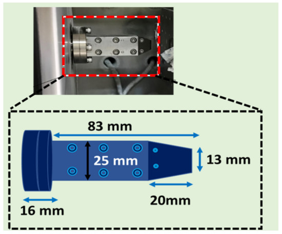
Figure 1.
Schematic and photograph showing the geometry of the nozzle used for the aerosol deposition.
Table 2.
Deposition parameters used for the ZnO films during AD process.
After aerosol deposition, the ZnO films obtained were dried at room temperature and characterized. X-ray diffraction (XRD) (RINT 2500, Rigaku, Tokyo, Japan) with a Cu Kα radiation (α = 1.54059 Å) was carried out to investigate the crystallinity of the films. The size of the ZnO crystallite was calculated using the Debye-Scherrer formula as shown in Equation (1) [37].
where D is the crystallite size (nm), β is the broadening of the diffraction line measured at half of its maximum (FWHM) intensity (rad.) and λ is the X-ray wavelength (1.5406 Å). The morphology and thickness of ZnO films were characterized using field emission scanning electron microscope (FESEM) (S-4800, HITACHI, Tokyo, Japan) at an accelerating voltage of 40 kV. The optical properties of ZnO films were evaluated using a UV–Visible spectrometer (V-670, JASCO Corporation, scanning range: 350–700 nm) and Raman spectroscope (NRS-3100, JASCO Corporation, Tokyo, Japan). The photoluminescence (PL) characteristics were investigated using a He-Cd laser (KIMMON KOHA, Tokyo, Japan, excitation wavelength, λ = 325 nm) as an excitation source, and the spectra were recorded using a monochromator (Nikon G250, Tokyo, Japan).
2.2. Fabrication of DSSCs Using the AZ Films
The aerosol-deposited ZnO films on FTO glass substrates were used as working electrodes (WEs) in the fabrication of DSSCs. Firstly, the WEs were immersed in 0.3 mM of N719 dye/ethanol solution for 24 h in dark condition. Next, the WEs were rinsed with distilled water for three times and dried at room temperature. As for the counter electrode (CE), platinum (Pt) coated FTO glass substrates were used. A sandwich-type configuration was used for the fabrication of DSSCs as shown in Figure 2. The two electrodes (WE and CE) were sealed with the thermal adhesive (50 μm thick) and heated at about 100 °C on the hot plate to perfectly assemble the two electrodes together. Iodide/triiodide (I/I3) was used as an electrolyte prepared by mixing 0.05 M of iodide (WAKO, Osaka, Japan) into 50 mL acetonitrile. After that, 0.1 M of lithium iodide (WAKO, Osaka, Japan), 0.6 M of 1,2-di-mehtyl-3-proylimidazolium iodide (WAKO, Osaka, Japan) and 0.5 M of 4-tert-butylpyridine (WAKO, Osaka, Japan) were add and stirred until homogeneous solution were obtained at room temperature. The electrolyte was injected into the sealed electrodes through the small opening holes at the CE. Finally, the AZ DSSC was sealed using polytetrafluorethylene sealant to prevent leakage of the electrolyte solution. The current density-voltage (J-V) curves were measured using an ADCMT 6244 DC Voltage/Current Source/Monitor and an HAL–320 W solar simulator (Asahi spectra) with a 300 W Xenon Lamp and an air-mass 1.5 global filter was used for light irradiation. The incident light intensity and the active area were kept at 100 mW/cm2 and 1 (1 × 1) cm2, respectively.
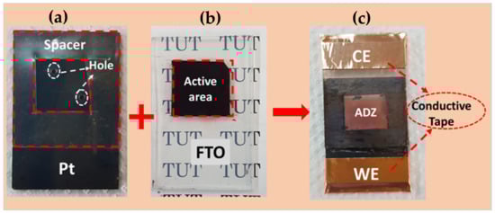
Figure 2.
Photographs showing the (a) Pt counter electrode (CE), (b) N719-sensitized working electrode (WE) and (c) fabricated sandwich-type ZnO film based DSSCs.
3. Results and Discussion
3.1. Crystallinity of the AZ Thin Films
Figure 3 shows the XRD diffraction pattern of raw ZnO powder and the aerosol-deposited ZnO films. The XRD peaks at the diffraction angles of 31.55°, 34.20°, 36.04°, 47.33°, 56.39°, 62.67°, 66.19°, 67.76°, 68.90°, 72.3° and 76.78° correlate to (100), (002), (101), (012), (110), (103), (200), (112), (210), (004), and (202) planes of ZnO hexagonal wurtzite structure (JCPDS- 96-901-1663). Peaks from the FTO substrates were also detected at 26.50°, 33.74°, 37.86°, 51.80°, 54.66°, 61.74°, and 65.69° correspond to the (110), (011), (020), (121), (220), (130) and (031) planes of tin (IV) oxide (JCPDF-98-006-3707), respectively. No significant shift on the 2θ of the diffraction peaks of ZnO films as compared to ZnO powder, suggesting that the films have identical crystal quality. A few additional diffraction peaks were found, matching with Zn-SnO (JCPDF-96-101-0111). The presence of this secondary phase, i.e., Zn-SnO, suggests the formation of a new compound during the AZ deposition. The secondary phase was likely from the interfaces between ZnO particles and FTO substrates. The energy released from the ZnO particles facilitated the formation of Zn-SnO at the contact points between ZnO particles and FTO substrate during the bombardment (deposition).
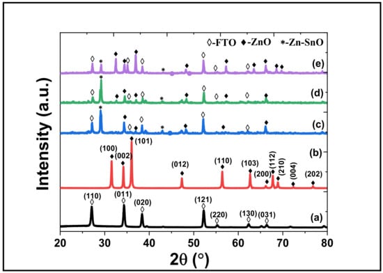
Figure 3.
X-ray diffraction pattern of (a) FTO, (b) raw ZnO powder, (c) AZ-I, (d) AZ-II and (e) AZ-III films.
The average crystallite size of ZnO powder was 43 nm. The average crystal size of ZnO films slightly increased to 45, 48 and 50 nm for AZ-I, AZ-II and AZ-III films, respectively as shown in Figure 4. The increment in crystallite size suggests that consolidation and recrystallization occurred during the AD process. The kinetic energy of ZnO powder could generate localized heating and energy conversion resulting in the growth of ZnO crystallites through densification and particle bonding when the powder impinges on the FTO glass substrate [38]. The continuous supply of kinetic energy with an increased number of cycles (three deposition cycles) could cause formation of higher crystallite size due to fusion of fine particle fragments.
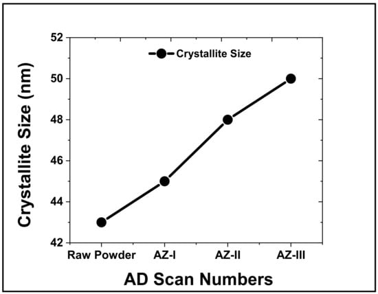
Figure 4.
Crystallize size of ZnO powder and the aerosol-deposited ZnO films.
3.2. Morphologies and Thickness of the Aerosol-Deposited ZnO Films
The effects of deposition cycles on the morphology and thickness of ZnO films were characterized using FESEM and the results are shown in Figure 5. From the SEM image shown in Figure 5a, a rather smooth, compact, and dense surface is observed with some remnant particles on the surface. The cross-sectional view in Figure 5b shows that the deposited ZnO film has a rather uniform thickness with an average of 271 ± 44 nm (n = 10). In the initial stage of AD, formation of a stable anchor layer at the substrate interface is important prior to subsequent deposition of dense film. During the anchor layer formation, a sufficient amount of independent particles plays a vital role in forming the initial anchoring layer [39]. More remnant agglomerated particles were also observed on the surface of AZ-II as highlighted in circles in Figure 5c. The thickness of ZnO film obtained was slightly reduced to 249 ± 51 nm as shown in Figure 5d. Further increase in the deposition cycle to three cycles led to the formation of large particle agglomerates as shown in Figure 5e. The surface appearance of the AZ-III films was less dense, with rough surfaces observed. The thickness of ZnO film was 258 ± 51 nm as shown in Figure 5f. From the cross-sectional SEM images shown in Figure 5f, the thickness was less uniform as compared to AZ-I and AZ-II. It is thought that the abrasion of the deposited ZnO films by the subsequent deposition cycle caused the reduction in thickness. During the aerosolization process in the rotating aerosol chamber, agglomeration of the ZnO particles occurred forming submicron-sized agglomerates due to Van der Waals interaction. The injection of agglomerated ZnO particles could cause film abrasion. Therefore, the thickness of the AZ films decreased during the second deposition cycle and increased slightly after the third deposition cycle as shown in Figure 6. Nevertheless, the slight increase in thickness of AZ-III could be due to process variation, or the formation of many agglomerated particles that are observed on the surface of AZ-III as shown in Figure 5e,f.
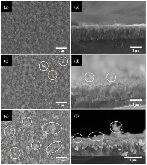
Figure 5.
FESEM images showing the surface morphology of (a) AZ-I, (c) AZ-II, (e) AZ-III films, and cross-sectional view of (b) AZ-I, (d) AZ-II and (f) AZ-III films produced under different deposition cycles.
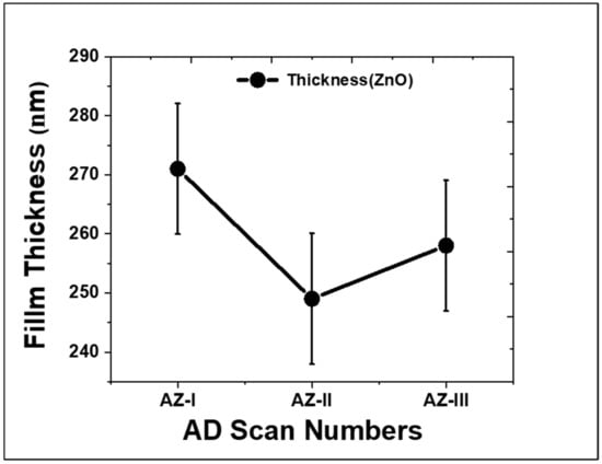
Figure 6.
The thickness of ZnO films obtained with different deposition cycles.
The reduction in thickness and the generation of rough surface due to particles’ agglomeration of the surface of the deposited ZnO films could be elucidated as the schematic shown in Figure 7. The subsequent bombardment of ZnO particles onto the film could cause etching and abrasion of the outermost layer during the 2nd cycle or 3rd cycle. With a prolonged cycle, ZnO particle agglomeration is thought to occur during the aerosolization process. These agglomerates would cause higher momentum transfer resulting in surface abrasion or etching. The rough surface and loose particles found particularly on the surface of AZ films which are shown in Figure 5c,e, are illustrated and shown as Figure 7b,c. The abrasion of the surface by ZnO particles or agglomerates caused the generation of particle agglomerates and coarse surface after repetitive cycles. This observation is aligned with the finding of Gurav et. al. as they mentioned that the film thickness is influenced by factors such as the transport of the aerosol droplets to the substrate, concentration of particles used and aggregation of the aerosol droplet [40].
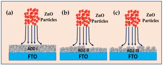
Figure 7.
Schematic representing the formation of ZnO films using the AD method under different deposition cycles (a) AZ-I, (b) AZ-II, and (c) AZ-III.
3.3. Optical Properties of the AZ Films
Figure 8 shows the UV-Vis results of the ZnO films obtained using different deposition cycles. The adsorption spectrum was recorded in the wavelength range 200–800 nm. All the ZnO films exhibited UV absorbance at wavelengths of less than 400 nm. The AZ-I film exhibited an absorption edge at 325 nm. As for the AZ-II and AZ-III, the UV absorbance edge was at 432 nm and 339 nm, respectively. The result indicates that the optical properties of the ZnO films change with the number of deposition cycles. During AD process, fragmentation of the raw particles could cause a reduction in the crystallites (1/10th of the original raw material particles) [29]. Therefore, as the size of the ZnO used in this study was approximately 100 nm, it is thought that particle fragments generated could have resulted in different optical properties due to the abovementioned phenomenon.
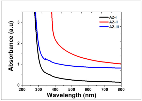
Figure 8.
Absorbance spectra of the aerosol deposited ZnO films obtained using different cycles.
The shift in absorbance edge of UV for the ZnO films may be caused by the defects generated within the ZnO crystals during the high impact collision during the RTIC. The presence of defects in ZnO films, which act as recombination centres, can be identified using room temperature photoluminescence (RTPL). Figure 9a shows the RTPL spectra of the aerosol-deposited ZnO films, which exhibited a typical near band edge emission (NBE) at approximately ~380 nm and a broad visible light emission (deep level emission, DLE). The NBE is associated with the release of energy due to transition of electrons from the conduction band (CB) to valence band (VB) of ZnO [41]. The maximum peak of NBE for the ZnO films produced at one, two and three deposition cycles are 387, 384 and 383 nm, respectively. In addition, the intensity of NBE was not dominant for all the ZnO films, suggesting a rather low crystallinity of ZnO films.
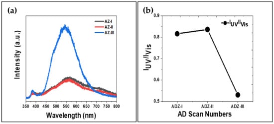
Figure 9.
(a) RTPL spectra of the aerosol-deposited ZnO films, and (b) IUV/IVis ratio.
On the other hand, the dominant DLEs observed are defect related emissions. The excited charge carriers recombination at the crystal defects would then produce luminescence signals with less energy than the band gap energy [42]. The DLE of ZnO could originate from oxygen interstitials (Oi), oxygen vacancies (VO), oxygen substitution in Zn site (OZn), Zn interstitials (Zni), Zn vacancies (VZn), or Zn substitution in the oxygen site (ZnO) [43]. In this study, the maximum peaks of DLE for AD-I, AD-II and AD-III are 558, 560 and 541 nm, respectively. The green emission, i.e., 558–560 nm obtained is associated with oxygen vacancies (VO) in the ZnO films [44], whereas the yellow emission (541 nm) was related to the interstitial oxygen (Oi) [45]. The strong emission intensity of the AZ-III sample in the visible region indicates an existence of high defects concentration in the ZnO film. This could be caused by repetitive collisions during AD that generated the crystal defects, loose agglomerated particles and rough film’s surface as shown in Figure 5e,f. Figure 9b shows the ratio of UV peak intensity to visible light emission intensity (IUV/IVis). A low IUV/IVis ratio indicates that the ZnO films possess poor crystal quality. In comparison, the AZ-III sample exhibited the lowest crystal quality as the smallest IUV/IVis ratio (0.53) was obtained while the IUV/IVis for AD-I and AD-II are comparable (0.82 and 0.84).
3.4. Photoconversion Efficiency of the DSSCs Fabricated Using the AZ Films
The AZ films obtained were used for DSSCs fabrication and the photoconversion efficiency was evaluated. Figure 10a shows the J-V curves of the fabricated DSSCs using AZ films with different deposition cycles. From Figure 10a, the current density of the DSSCs obtained using AZ-I, AZ-II and AZ-III are 1.64, 4.62 and 0.70 mA cm−2, respectively. The highest current density is obtained using the AZ-II sample indicating a rather dense ZnO film generating a better electron conductive pathway for the photogenerated electron from the ZnO to the FTO substrate. Severe abrasion and the presence of ZnO particle agglomerates resulted in the lowest current density of 0.70 mA cm−2 as the poor interparticle connectivity could lead to electron recombination. Similar phenomenon has been reported by Cho and Yoon using aerosol-deposited TiO2 porous films and subsequent heat treatment of the films (at 450 °C) improved the connectivity of the particles leading to higher PCE [46].
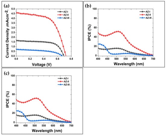
Figure 10.
(a) J-V curves, (b) photoconversion efficiency (PCE) and (c) IPCE obtained using the fabricated AZ-DSSCs.
The photoconversion efficiency (PCE) % was determined using the following Equation (2):
where, JSC is the short circuit photocurrent density, VOC is the open circuit photovoltage, FF is the fill factor and Pin is the incident light density (100 m W/cm2).
The calculated PCE % of the AZ films are shown and compared in Figure 10b. The PCE % obtained increased from 0.73 to 1.78% when the deposition cycle was increased from one (AZ-I) to two (AZ-II). However, the PCE % deteriorated to 0.19% after the three deposition cycles (AZ-III). The result indicates that the formation of less dense ZnO film with agglomerated particles on the surface of the AZ-III sample resulted in a poor PCE of the DSSC. A dense and compact aerosol-deposited ZnO film can suppress electron-hole recombination during PCE evaluation. In a study reported by Cho and Yoon, they investigated the DSSCs performance of aerosol-deposited multilayer titanium dioxide (TiO2) films and the effect of a compact TiO2 layer [46]. They demonstrated that a presence of compact TiO2 layer between FTO substrate and subsequent TiO2 film deposition resulted in higher DSSC performance due to a reduced electron recombination. It is noteworthy that a mixture of TiO2 particles with the size of 700 and 25 nm were used while the thickness of aerosol-deposited TiO2 films obtained in their study ranged from 15~17 µm. Moreover, the repetitive bombardment of ZnO particles could have caused abrasion and generated crystal defects that adversely affected the PCE of the assembled DSSC. The crystal defects in the AZ-III film, i.e., interstitial oxygen (Oi), which are determined from the RTPL analysis, indicate that electron-hole recombination at these defects led to significant deterioration of the PCE.
Figure 10c shows the incident-photon-to-current conversion efficiency (IPCE) curves obtained as a function of excitation wavelengths between 400–700 nm using the assembled DSSCs. The curves indicate the active IPCE response of the AZ films. The IPCE of the AZ-II samples exhibited a maximum IPCE at wavelength of 510 nm, with a 52% IPCE using the AZ-II sample. The IPCE result is consistent with the UV-Vis results obtained in Figure 8, indicating that the AZ-II sample possesses the best absorbance compared to AZ-I and AZ-III samples. Table 3 summarizes AZ films based DSSCs versus its structural, electrical, optical, and photovoltaic performance by various deposition cycles. The findings from this study indicates that aerosol-deposited ZnO films can be used for DSSC. Although further optimization, elucidation and control deposition of desired AD films are still required, the feasible rapid film deposition at room temperature possesses good potential for future development of scalable and affordable solar cells.
Table 3.
A summary of the properties obtained using the AZ-DSSCs.
4. Conclusions
The AD method is a simple, rapid film deposition method at room temperature, in which ZnO films could be formed by direct bombardment of accelerated ZnO powder onto the FTO substrates. In this study, the effect of deposition cycles on the thickness and optical properties of the AZ films was first investigated. Next, the DSSCs’ PCE using the AZ films were evaluated. The PCE increased from 0.73% to 1.78% with an increased deposition cycle from one (AZ-I) to two (AZ-II) cycles. However, the PCE % decreased to 0.19% when the AZ-III film (three cycles) was used due to the formation of loose particle agglomerates on the surface and a reduced thickness of aerosol-deposited ZnO film. The result indicated that abrasion of deposited ZnO thin film occurred with subsequent deposition cycles. The AZ-III contained crystal defects as indicated by the small IUV/IVis ratio (0.53) in the RTPL analysis. The findings from this study could be beneficial for further development of scalable DSSCs using the AD method with low environmental impact (without high temperature annealing) and film deposition on substrates with low melting points.
Author Contributions
Conceptualization, M.Z.T. and W.K.T.; methodology, M.Z.T. and W.K.T.; formal analysis, M.Z.T. and S.-Y.P.; investigation, M.Z.T.; resources, W.K.T., G.K. and H.M.; writing—original draft preparation, M.Z.T.; writing—review and editing, W.K.T., H.M., G.K., A.M. and S.-Y.P.; supervision, S.-Y.P. and A.M.; funding acquisition, S.-Y.P., W.K.T. and H.M. All authors have read and agreed to the published version of the manuscript.
Funding
This research was funded by AUN/SEED-Net grant number 304.PBAHAN.6050390/J135 and The Japan Society for the Promotion of Science (JSPS) KAKENHI Grant Number 18H05452, 22H01790 and 22K04737.
Institutional Review Board Statement
Not applicable.
Informed Consent Statement
Not applicable.
Data Availability Statement
The data presented in this study are available upon request.
Acknowledgments
The authors want to express appreciation for the financial support from AUN/SEED-Net (Grant number: 304.PBAHAN.6050390/J135) and The JSPS KAKENHI Grant Number 18H05452, 22H01790 and 22K04737. Hiroto Sekiguchi of the Toyohashi University of Technology is acknowledged for the photoluminescence measurements.
Conflicts of Interest
The authors declare no conflict of interest.
References
- Spencer, J.A.; Mock, A.L.; Jacobs, A.G.; Schubert, M.; Zhang, Y.; Tadjer, M.J. A review of band structure and material properties of transparent conducting and semiconducting oxides: Ga2O3, Al2O3, In2O3, ZnO, SnO2, CdO, NiO, CuO, and Sc2O3. Appl. Phys. Rev. 2022, 9, 011315. [Google Scholar] [CrossRef]
- Li, F.; Yu, Y.; Xu, C.; Li, Y.; He, Z.; Bi, X. Atomic-Layer-Deposited ZnO/Al2O3 Nanolaminates for White-Light-Emitting Diodes. ACS Appl. Nano Mater. 2022, 5, 8730–8734. [Google Scholar] [CrossRef]
- Lan, Y.; Yang, G.; Zhao, Y.; Liu, Y.; Demir, A. Facet passivation process of high-power laser diodes by plasma cleaning and ZnO film. Appl. Surf. Sci. 2022, 596, 153506. [Google Scholar] [CrossRef]
- Choi, H.; Kim, K.; Kim, M.; Kim, J.D.; Cho, I.; Kim, I.; Chae, H.; Han, I.; Kim, H.; Seo, J.H.; et al. Solution-Processable Ag-Mediated ZnO Nanowires for Scalable Low-Temperature Fabrication of Flexible Devices. ACS Appl. Electron. Mater. 2022, 4, 910–916. [Google Scholar] [CrossRef]
- Adesoye, S.; Dellinger, K. ZnO and TiO2 nanostructures for surface-enhanced Raman scattering-based bio-sensing: A review. Sens. Bio-Sens. Res. 2022, 37, 100499. [Google Scholar] [CrossRef]
- Badgujar, A.C.; Yadav, B.S.; Jha, G.K.; Dhage, S.R. Room Temperature Sputtered Aluminum-Doped ZnO Thin Film Transparent Electrode for Application in Solar Cells and for Low-Band-Gap Optoelectronic Devices. ACS Omega 2022, 7, 14203–14210. [Google Scholar] [CrossRef]
- Kumar, R.R.; Shukla, R.; Pandey, S.K. Impact of radio frequency power on the optoelectronic properties of ZnO films. Opt. Quantum Electron. 2022, 54, 1–9. [Google Scholar] [CrossRef]
- Singh, J.; Srivastava, A. Morphological evolution and its correlation with optical and field emission properties in pulsed laser deposited ZnO nanostructures. Mater. Sci. Semicond. Process. 2022, 138, 106282. [Google Scholar] [CrossRef]
- Pung, S.-Y.; Choy, K.-L.; Hou, X. Tip-growth mode and base-growth mode of Au-catalyzed zinc oxide nanowires using chemical vapor deposition technique. J. Cryst. Growth 2010, 312, 2049–2055. [Google Scholar] [CrossRef]
- Shkir, M. Enhancement in optical and electrical properties of ZnO thin films via Co doping for photodetector applications. Mater. Sci. Eng. B 2022, 284, 115861. [Google Scholar] [CrossRef]
- Alshammari, A.S.; Khan, Z.R.; Gandouzi, M.; Mohamed, M.; Bouzidi, M.; Shkir, M.; Alshammari, H.M. Tailoring the optical properties and the UV detection performance of sol-gel deposited ZnO nanostructured thin films via Cd and Na co-doping. Opt. Mater. 2022, 126, 112146. [Google Scholar] [CrossRef]
- Gueddouch, K.; Zidane, M.; Temsamani, R.; Mrigal, A.; Addou, M.; Ettami, S. Structural, optical and electrical properties of F doped ZnO films: Experimental and theoretical study. Mater. Today Proc. 2022, 66, 151–157. [Google Scholar] [CrossRef]
- Althobaiti, M.; Alotaibi, A.A.; Alharthi, S.S.; Badawi, A. Modification of the structural, linear and nonlinear optical properties of zinc oxide thin films via barium and magnesium doping. Opt. Mater. 2022, 131, 112646. [Google Scholar] [CrossRef]
- Fiaz Khan, M.; Siraj, K.; Anwar, M.S.; Irshad, M.; Hussain, J.; Faiz, H.; Majeed, S.; Dosmailov, M.; Patek, J.; Pedarnig, J.D.; et al. 700 keV Ni+2 ions Induced Modification in Structural, Surface, Magneto-Optic and Optical Properties of ZnO Thin Films. Nucl. Instrum. Methods Phys. Res. B Beam Interact. Mater. Atoms 2016, 368, 45–49. [Google Scholar] [CrossRef]
- Toe, M.; Jusoh, N.; Pung, S.; Yaacob, K.; Matsuda, A.; Tan, W.; Han, S. Effect of ZnO Seed Layer on the Growth of ZnO Nanorods on Silicon Substrate. Mater. Today Proc. 2019, 17, 553–559. [Google Scholar] [CrossRef]
- Tan, W.K.; Muto, H.; Ito, T.; Kawamura, G.; Lockman, Z.; Matsuda, A. Facile Fabrication of Plasmonic Enhanced Noble-Metal-Decorated ZnO Nanowire Arrays for Dye-Sensitized Solar Cells. J. Nanosci. Nanotechnol. 2020, 20, 359–366. [Google Scholar] [CrossRef]
- Tan, W.K.; Ito, T.; Kawamura, G.; Muto, H.; Lockman, Z.; Matsuda, A. Controlled facile fabrication of plasmonic enhanced Au-decorated ZnO nanowire arrays dye-sensitized solar cells. Mater. Today Commun. 2017, 13, 354–358. [Google Scholar] [CrossRef]
- Toe, M.Z.; Pung, S.-Y.; Yaacob, K.A.B.; Han, S.S. Effect of Dip-Coating Cycles on the Structural and Performance of ZnO Thin Film-based DSSC. Arab. J. Sci. Eng. 2021, 46, 6741–6751. [Google Scholar] [CrossRef]
- Sonklin, T.; Munthala, D.; Leuasoongnoen, P.; Janphuang, P.; Pojprapai, S. Effect of substrate-tilting angle-dependent grain growth and columnar growth in ZnO film deposited using radio frequency (RF) magnetron sputtering method. J. Mater. Sci. Mater. Electron. 2022, 33, 16977–16986. [Google Scholar] [CrossRef]
- Wang, J.; Wang, L. Morphology and Field Emission of ZnO Nanomaterials at Different Positions. JAMP 2022, 10, 1028–1035. [Google Scholar] [CrossRef]
- Pung, S.-Y.; Choy, K.-L.; Hou, X.; Shan, C. Preferential growth of ZnO thin films by the atomic layer deposition technique. Nanotechnology 2008, 19, 435609. [Google Scholar] [CrossRef]
- Fasquelle, D.; Députier, S.; Bouquet, V.; Guilloux-Viry, M. Effect of the Microstructure of ZnO Thin Films Prepared by PLD on Their Performance as Toxic Gas Sensors. Chemosensors 2022, 10, 285. [Google Scholar] [CrossRef]
- Kouhestanian, E.; Ranjbar, M.; Mozaffari, S.; Salaramoli, H. Investigating the Effects of Thickness on the Performance of ZnO-Based DSSC. Prog. Color. Color. Coat. 2021, 14, 101–112. [Google Scholar]
- Sheriff, M.H.; Murugan, S.; Manivasaham, A.; Kumar, R.A. Electro spray technique to enhance the physical property of sulphur doped zinc oxide thin film. Mater. Today Proc. 2021, 47, 1717–1723. [Google Scholar] [CrossRef]
- Pham, A.T.T.; Van Hoang, D.; Nguyen, T.H.; Le, O.K.T.; Wong, D.P.; Kuo, J.-L.; Chen, K.-H.; Phan, T.B.; Tran, V.C. Hydrogen enhancing Ga doping efficiency and electron mobility in high-performance transparent conducting Ga-doped ZnO films. J. Alloys Compd. 2021, 860, 158518. [Google Scholar] [CrossRef]
- Abdullah, H.; Ariyanto, N. Structural and optical properties of ZnO thin films for dye-sensitized solar cell. J. Appl. Sci. 2014, 14, 965–968. [Google Scholar] [CrossRef]
- Mahadik, S.A.; Pathan, H.M.; Salunke-Gawali, S.; Butcher, R.J. Aminonaphthoquinones as photosensitizers for mesoporous ZnO based dye-sensitized solar cells. J. Alloys Compd. 2020, 845, 156279. [Google Scholar] [CrossRef]
- Chawla, A.K.; Kaur, D.; Chandra, R. Structural and optical characterization of ZnO nanocrystalline films deposited by sputtering. Opt. Mater. 2007, 29, 995–998. [Google Scholar] [CrossRef]
- Akedo, J. Room temperature impact consolidation and application to ceramic coatings: Aerosol deposition method. J. Ceram. Soc. Jpn. 2020, 128, 101–116. [Google Scholar] [CrossRef]
- Tan, W.K.; Shigeta, Y.; Yokoi, A.; Kawamura, G.; Matsuda, A.; Muto, H. Investigation of the anchor layer formation on different substrates and its feasibility for optical properties control by aerosol deposition. Appl. Surf. Sci. 2019, 483, 212–218. [Google Scholar] [CrossRef]
- Eckstein, U.; Khansur, N.H.; Urushihara, D.; Asaka, T.; Kakimoto, K.-I.; Fey, T.; Webber, K.G. Defect modulated dielectric properties in powder aerosol deposited ceramic thick films. Ceram. Int. 2022, 48, 3308–33091. [Google Scholar] [CrossRef]
- Zhuo, F.; Eckstein, U.R.; Khansur, N.H.; Dietz, C.; Urushihara, D.; Asaka, T.; Kakimoto, K.; Webber, K.G.; Fang, X.; Rödel, J. Temperature-induced changes of the electrical and mechanical properties of aerosol-deposited BaTiO3 thick films for energy storage applications. J. Am. Ceram 2022, 105, 4108–4121. [Google Scholar] [CrossRef]
- Nadaud, K.; Sadl, M.; Bah, M.; Levassort, F.; Ursic, H. Effect of thermal annealing on dielectric and ferroelectric properties of aerosol-deposited 0.65 Pb (Mg1/3Nb2/3) O3-0.35 PbTiO3 thick films. Appl. Phys. Lett. 2022, 120, 112902. [Google Scholar] [CrossRef]
- Teshima, S.; Ono, Y.; Goto, N.; Inada, R. Electrical conducting properties of Na2Zn2TeO6 thick films fabricated by aerosol deposition. Mater. Lett. 2022, 324, 132640. [Google Scholar] [CrossRef]
- Hahn, B.-D.; Lee, J.-M.; Park, D.-S.; Choi, J.-J.; Ryu, J.; Yoon, W.-H.; Lee, B.-K.; Shin, D.-S.; Kim, H.-E. Aerosol deposition of silicon-substituted hydroxyapatite coatings for biomedical applications. Thin Solid Films 2010, 518, 2194–2199. [Google Scholar] [CrossRef]
- Toe, M.Z.; Tan, W.K.; Muto, H.; Kawamura, G.; Matsuda, A.; Yaacob, K.A.B.; Pung, S.-Y. Effect of Carrier Gas Flow Rates on the Structural and Optical Properties of ZnO Films Deposited Using an Aerosol Deposition Technique. Electron. Mater. 2022, 3, 27. [Google Scholar] [CrossRef]
- Holzwarth, U.; Gibson, N. The Scherrer equation versus the ‘Debye-Scherrer equation’. Nat. Nanotechnol. 2011, 6, 534. [Google Scholar] [CrossRef]
- Ravichandran, K.; Vasanthi, M.; Thirumurugan, K.; Sakthivel, B.; Karthika, K. Annealing induced reorientation of crystallites in Sn doped ZnO films. Opt. Mater. 2014, 37, 59–64. [Google Scholar] [CrossRef]
- Exner, J.; Hahn, M.; Schubert, M.; Hanft, D.; Fuierer, P.; Moos, R. Powder requirements for aerosol deposition of alumina films. Adv. Powder Technol. 2015, 26, 1143–1151. [Google Scholar] [CrossRef]
- Gurav, A.; Kodas, T.; Pluym, T.; Xiong, Y. Aerosol Processing of Materials. Aerosol Sci. Technol. 1993, 19, 411–452. [Google Scholar] [CrossRef]
- Tan, W.K.; Kawamura, G.; Muto, H.; Razak, K.A.; Lockman, Z.; Matsuda, A. Blue-emitting photoluminescence of rod-like and needle-like ZnO nanostructures formed by hot-water treatment of sol–gel derived coatings. J. Lumin 2015, 158, 44–49. [Google Scholar] [CrossRef]
- Janotti, A.; Van de Walle, C.G. Native point defects in ZnO. Phys. Rev. B 2007, 76, 165202. [Google Scholar] [CrossRef]
- Aziz, S.N.Q.A.A.; Meng, K.C.; Pung, S.-Y.; Lockman, Z.; Ul-Hamid, A.; Tan, W.K. Rapid growth of zinc oxide nanorods on kanthal wires by direct heating method and its photocatalytic performance in pollutants removal. J. Ind. Eng. Chem. 2022, 118, 226–238. [Google Scholar] [CrossRef]
- Wang, J.; Chen, R.; Xiang, L.; Komarneni, S. Synthesis, properties and applications of ZnO nanomaterials with oxygen vacancies: A review. Ceram. Int. 2018, 44, 7357–7377. [Google Scholar] [CrossRef]
- Wu, X.L.; Siu, G.G.; Fu, C.L.; Ong, H.C. Photoluminescence and cathodoluminescence studies of stoichiometric and oxygen-deficient ZnO films. Appl. Phys. Lett. 2001, 78, 2285–2287. [Google Scholar] [CrossRef]
- Cho, S.H.; Yoon, Y.J. Multi-layer TiO2 films prepared by aerosol deposition method for dye-sensitized solar cells. Thin Solid Films 2013, 547, 91–94. [Google Scholar] [CrossRef]
Disclaimer/Publisher’s Note: The statements, opinions and data contained in all publications are solely those of the individual author(s) and contributor(s) and not of MDPI and/or the editor(s). MDPI and/or the editor(s) disclaim responsibility for any injury to people or property resulting from any ideas, methods, instructions or products referred to in the content. |
© 2023 by the authors. Licensee MDPI, Basel, Switzerland. This article is an open access article distributed under the terms and conditions of the Creative Commons Attribution (CC BY) license (https://creativecommons.org/licenses/by/4.0/).