Article

Variable Multiple Interleaved Bi-Directional DC/DC Converter with Current Ripple Optimization

1
Department of Electrical Engineering, Harbin Institute of Technology, Harbin 150001, China
2
Yantai Research Institute, Harbin Engineering University, Yantai 265615, China
*
Author to whom correspondence should be addressed.
Appl. Sci. 2023, 13(3), 1744; https://doi.org/10.3390/app13031744
Submission received: 27 December 2022 / Revised: 20 January 2023 / Accepted: 27 January 2023 / Published: 29 January 2023
(This article belongs to the Special Issue Progress in Electrical Energy Storage System)

Abstract

:
In order to reduce the current ripple and improve the power density of the system, the multiple structure design is generally adopted by the traditional bidirectional DC/DC converter. However, the fixed multiplicity design can’t make the DC/DC power converter always output the smallest current ripple under different duty ratios. Through this research, it is found that the current ripple is related to duty cycle and parallel multiplicity, and then a variable multiplicity bidirectional DC/DC power converter is proposed. Firstly, the relationship between the current ripple and parallel multiplicity and duty cycle is deduced, and the basic topology of variable multiplicity bidirectional DC/DC power converter is determined; Secondly, the average value model and AC small signal model of the system are established based on the topological structure, and then the state equation is obtained. Thirdly, the current compensation control method is designed based on the state equation. Finally, the experimental platform of variable multiplicity bidirectional DC/DC power converter is built.

1. Introduction

Energy storage systems have been widely used to improve the power distribution between renewable power generation, large power grids, and user loads [1,2,3]. As the power transmission channel between the DC bus and the energy storage system, the bidirectional DC/DC converter can realize bidirectional energy flow and improve energy distribution efficiency [4,5,6]. However, the DC/DC converter may introduce a large current ripple to the DC bus, which affects the quality of the power supply [7,8].
Many researchers have proposed different methods to reduce the current ripple, each of which has its adpply [7,8].
Many researchers have proposed different methods to reduce the current ripple, each of which has its advantages [9,10,11]. At present, the current ripple optimization methods of DC/DC converter mainly include: input parallel output series (IPOS) DC/DC converter, ripple current injection DC/DC converter, resonant ripple absorption DC/DC converter, DC/DC converter using coupled inductor technology, multiple DC/DC converter, etc. Reference [12] studied an IPOS DC/DC converter, which could offset the current ripple to a certain extent, but has the problem of low voltage gain. The DC/DC converter with ripple current injection proposed in [13] artificially injects ripple current at both ends of the inductor to eliminate the ripple current. The ripple suppression effect is good, but the circuit is more complicated. Reference [14] proposed a resonant ripple absorption DC/DC converter that uses the LC devices to generate resonance to optimize the current ripple, but the ripple suppression capability for dynamic loads is poor due to the fixed system parameters. The DC/DC converter with coupled inductor technology [15] replaces the inductor in the traditional DC/DC converter with a coupled inductor. When the coupling coefficient of the coupled inductor is selected reasonably, a better ripple suppression effect can be achieved, however, the switching stress is larger due to the influence of leakage inductance. The multiple DC/DC converter adopts multiple structure and has high power grade. The increase in converter multiplicity can reduce the current ripple, reduce the switching stress, improve the equivalent switching speed, improve the dynamic performance, and then improve the power quality [16,17,18,19,20,21,22,23].
The above current ripple optimization methods of DC/DC converters mainly have the problems of large switching stress and low voltage gain, so they are difficult to be applied to high power energy storage systems, while the traditional multiple DC/DC converters can not only reduce switching stress, but also achieve better current ripple suppression through continuous improvement, so they are widely used in high power energy storage systems [18,19]. Energy storage systems (especially battery energy storage systems) are highly sensitive to current ripples, and excessive current ripples will affect the service life of the system. Reducing the current ripple of the converter is of great significance for improving the quality of the power supply, prolonging the service life of the system. However, the existing research mostly studies improving the circuit structure of the multiplexed DC/DC converter to optimize the current ripple, such as using the coupled inductor instead of the traditional inductor [15] and using the new SiC device [24], the working model of the multiplexed converter is also limited to the fixed multiplicity model, and there are few studies on the influence of changing the parallel multiplicity on the current ripple. In fact, related researches find the multiplicity of parallel circuits also has an important influence on the magnitude of current ripple, and there is always a parallel multiplicity corresponding to the minimum current ripple under different duty cycle [20,21,22,23]. The main contribution of this paper is to propose a current ripple optimization method for bidirectional DC/DC converters by changing the multiplicity of parallel circuits. In reference [25], increasing the switching frequency can reduce the current ripple, but this will inevitably increase the loss and reduce the efficiency. The biggest feature of the method in this paper is that the actual operating multiplicity of the multiplexed DC/DC converter will be dynamically changed according to the duty cycle, as a result, the current ripple is optimized without changing the switching frequency. The improvements are shown as follows: Firstly, the relationship between the current ripple and parallel multiplicity and duty cycle is studied. Secondly, a control method that can change the parallel multiplicity of the DC/DC converter to optimize the current ripple is proposed. Thirdly, considering there are many similar circuits in the multiplex DC/DC converter, there will be the problem of uneven current distribution due to the differences in devices. Although automatic master control overcomes the vulnerability of the master-slave method, where the master is auto-selected by the maximum, it can trigger larger fluctuations in the output current [26]. In this paper, automatic master control and current compensation control are combined, compared with the single automatic master control, this method can better realize the current balance distribution and optimize fluctuations on the output current when the parallel multiple is switching.
This paper is organized as follows: In Section 2, the relationship between the current ripple and parallel multiplicity and duty cycle is deduced, and the basic topology of variable multiplicity bidirectional DC/DC power converter is determined. In Section 3, the average value model and AC small signal model of the system are established. In Section 4, the current compensation control is designed. In Section 5, the simulation model and the experimental platform of variable multiplicity interleaving bidirectional DC/DC power converter is built. The simulation and experiment results show that the optimization of the current ripple of the variable multiplicity bidirectional DC/DC converter is obvious.

2. The Principle of Current Ripple Optimization

Assuming that the bidirectional DC/DC converter operates in Buck mode, the topology of the converter is shown in Figure 1.
The relationship among load-side voltage ULoad, DC bus voltage, and duty cycle D is shown as follows:
V Load = D V DC
For inductance L, the slope of the current rising phase is defined as kup, and the slope of the current decreasing phase is defined as kdown.
k up = V DC V Load L k down = V Load L
In same-phase driving mode, iL1, iL2, iL3, iL4, and so on are exactly equal, then the peak-to-peak value of the ripple of total current can be shown as:
Δ i Ls = Δ i L 1 + Δ i L 2 + + Δ i Ln = n D k up T
In the phase-shift control, the relationship between the current and time is established by setting the current iL1 as the zero point at the initial time of a switching cycle [0,T]. The current iL1, iL2, iL3, iL4, and so on are shown in Figure 2.
Assuming that the slope of ndown-fold inductor current at the initial stage is kdown, and satisfies ndown + nup =n. Then the following relationship can be obtained.
1 D n 1 = n down D n + 1 = n up
Then, the duty cycle has the following relationship: 1 n down + 1 n D 1 n down n . Assuming that D is 50%, and n down = n 2 or n down = n 1 2 can be obtained according to the parity of n.
The expression of the first inductance current is shown as:
i L 1 = k up t t 0 , D T i L 1 = k down t T t D T , T
The expression of the second inductance current can be shown as:
i L 2 = k down · t T n t 0 , T n i L 2 = k up · t T n t T n , D T + T n i L 2 = k down · t n + 1 n T t D T + T n , T
The expression of the third inductance current can be shown as:
i L 3 = k down · t 2 T n t 0 , 2 T n i L 3 = k up · t 2 T n t 2 T n , D T + 2 T n i L 3 = k down · t n + 2 n T t D T + 2 T n , T
The expression of the n-th inductance current can be shown as:
i Ln = k up · t + T n t 0 , D T T n i Ln = k down · t n 1 n T t D T T n , n 1 n T i L 3 = k up · t n 1 n T t n 1 n T , T
According to Kirchhoff’s law, the expression of the iL in a switching cycle can be obtained and can be extended to the n-th cycle, which is shown in (9).
i L = n up k up + n down k down t+ n up k up T 2n n up 1 n down k down T 2n n down +1 t 0,DT n up 1 n T i L = n up 1 k up + n down +1 k down t + k up n up 1 n up 2 2n T k down n down +1 n down +2 2n T t DT n up 1 n T, T n i L = n up 1 k up + n down +1 k down t + k up n up 1 n up 4 2n T k down n down +1 n down +4 2n T t DT n up 2 n T, 2T n i L = n up k up + n down k down t + n up k up T 2n n up 2n+1 n down k down T 2n n down +2n1 t n1 n T,DT+ n down T n i L = n up 1 k up + n down +1 k down t + k up n up 1 n up 2n 2n T k down n down +1 n down +2n 2n T t DT+ n down T n ,T
According to (5)–(9) and Figure 2, when phase shift control is applied to the n-fold DC/DC converter, the total ripple of the current flowing through the inductor L is shown in (10):
Δ i Lm = n up k up + n down k down · D T n up 1 n T = T V DC L · 1 D D n + 1 D 1 D n 1 · D n D n + 1 + 1 n
Define kLm as the ripple coefficient, which is shown in (11).
k Lm = 1 D D n + 1 D 1 D n 1 · D n D n + 1 + 1 n
The expression of (11) can be rewritten to.
Δ i Lm = T V DC L · k Lm
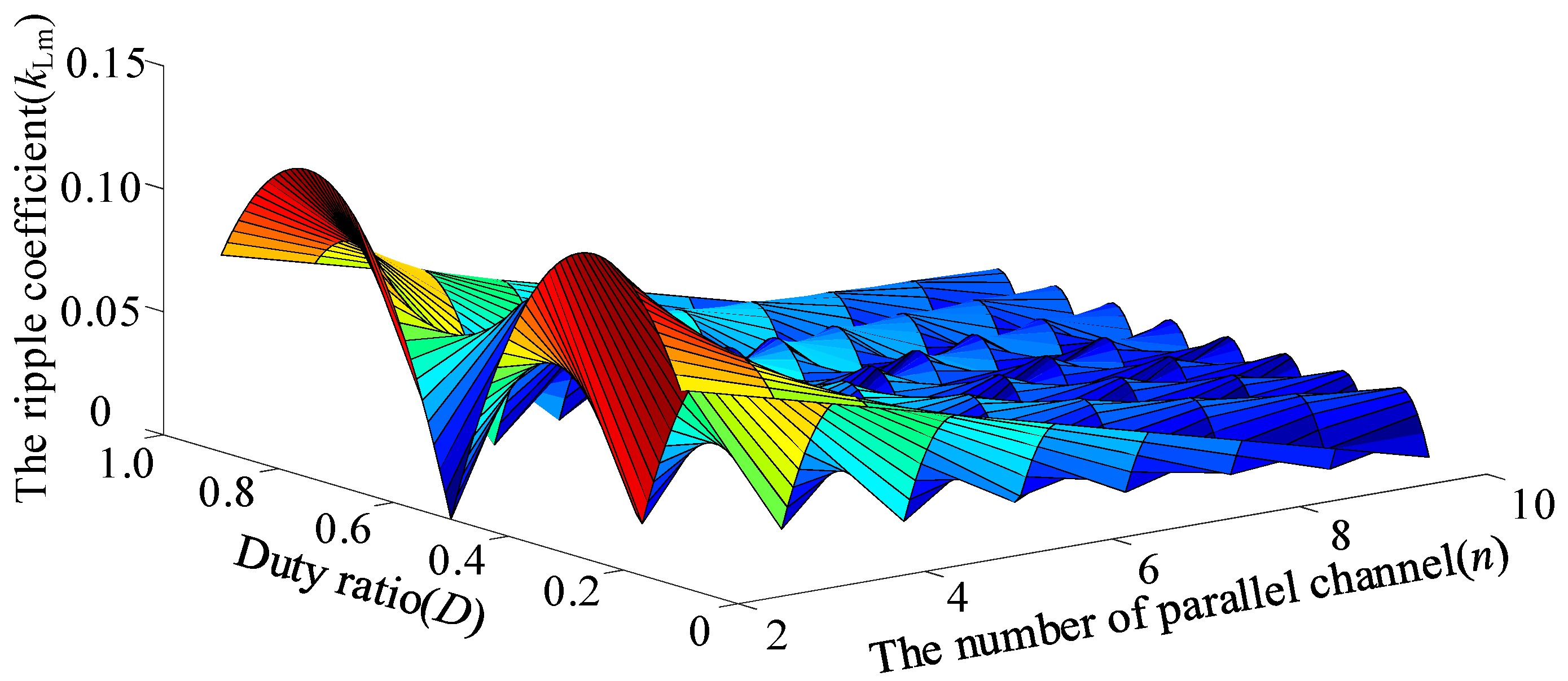
It can be seen from (11) that the ripple coefficient kLm is affected by the duty cycle D and the number of parallel multiplicity n. When the bidirectional DC/DC converter operates in Buck mode, the relationship between the ripple coefficient kLm, the duty cycle D, and the number of parallel channel multiplicity n is shown in Figure 3. It can be seen from Figure 3 that there is a point where the ripple coefficient kLm is 0 when different numbers of parallel multiplicity n and different duty cycle D are taken.
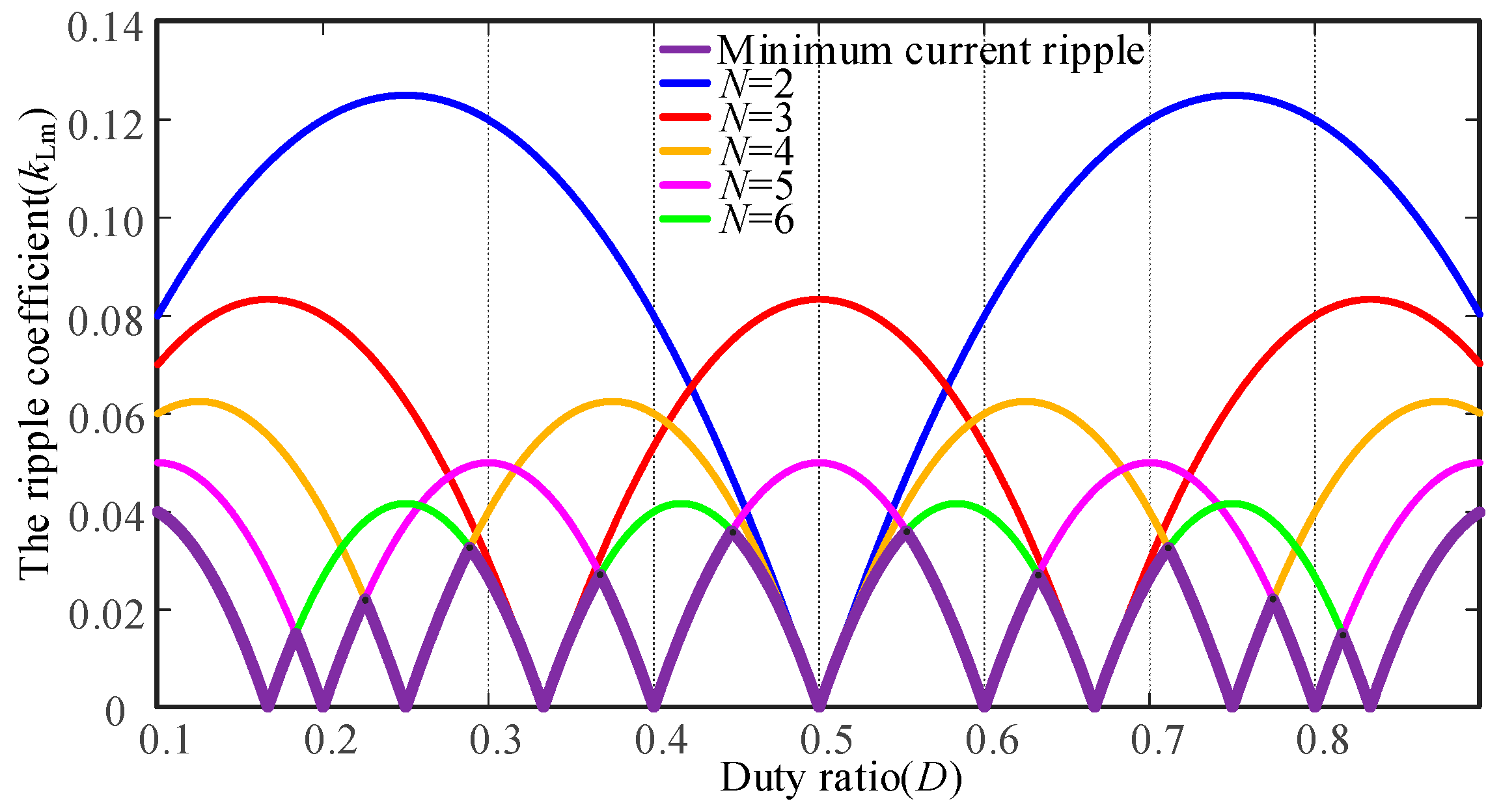
According to (11), the relationship between ripple coefficient kLm and duty cycle D can be obtained, shown in Figure 4, when the number of multiplicities is different. It can be seen from Figure 4 that there are n−1 points where the ripple coefficient is zero for the n-multiplicity bidirectional DC/DC power converter.
As can be seen from Figure 4, under the condition of different duty cycles, it is not that the more parallel multiplicity, the smaller the current ripple coefficient. Although the ripple coefficient generally decreases with the increase of parallel multiplicity, considering that too many parallel multiplicities will increase the complexity of the circuit; and more when the number of parallel multiplicities is greater than six, the increase of parallel multiplicity has no obvious effect on the reduction of current ripple. The principle of the variable multiplicity bidirectional DC/DC power converter is to automatically select the working number of parallel multiplicities according to the current duty cycles of the system. The number of parallel multiplicities that should be used for the minimum current ripple when the duty cycle is in the range of 0.1–0.9 is shown in Table 1. For example, when the duty cycle of the system is 0.25, the quadruple parallel structure should be adopted, and the controller outputs four PWM signals with a 90-degree phase shift in each multiplicity.
Figure 5 shows the number of parallel multiplicities that should be taken to minimize the current ripple. For example, when the duty cycle is 0.2, a five-fold parallel structure should be adopted, and the current ripple is the smallest; when the duty cycle is 0.25, a four-fold parallel structure should be adopted. Thus, a curve with the smallest current ripple can be obtained in Figure 5. By calculating the intersection point of the minimum current ripple carve in Figure 5, the corresponding relationship between the parallel multiplicity and the duty range can be obtained, as shown in Table 1.

3. The Model of Variable Multiplicity Interleaving Bidirectional DC/DC Power Converter

3.1. The Mean Value Model

In Figure 6, VDC is DC side voltage, iDC is DC side current, iLk (1 ≤ k ≤ n) is inductor current, Rk (1 ≤ k ≤ n) is the resistance of the inductor, VL is inductor voltage, VLoad is load-side voltage, iLoad is load-side current, and D is duty cycle.
The DC side current is shown as:
i DC = k = 1 n D k i Lk
When the lower arm is turned off and the upper arm is turned on, the voltages at both ends of each inductance can be shown as:
V L 1 = L 1 d i L 1 d t = V DC V Load i L 1 R 1 V L 2 = L 2 d i L 2 d t = V DC V Load i L 2 R 2 V Ln = L n d i Ln d t = V DC V Load i Ln R n
When the lower arm is turned on and the upper arm is turned off, the voltages at both ends of each inductance can be shown as:
V L 1 = L 1 d i L 1 d t = V Load i L 1 R 1 V L 2 = L 2 d i L 2 d t = V Load i L 2 R 2 V Ln = L n d i Ln d t = V Load i Ln R n
Because the switching period Ts is very small, it can be considered that VDC and VLoad are continuous and constant in a switching period. They can be expressed by their average values in a period.
V DC = V DC T s V Load = V Load T s
According to the volt-ampere characteristics and volt-second balance principle of the inductor, the average voltage of the inductor shown in (17) in a switching cycle can be obtained by dealing with Equations (14)–(16).
v L 1 t T s = 1 T s 0 D 1 T s v L 1 t d t + D 1 T s T s v L 1 t d t = D 1 V DC T s V Load T s i L 1 T s R 1 v L 2 t T s = 1 T s 0 D 2 T s v L 2 t d t + D 2 T s T s v L 2 t d t = D 2 V DC T s V Load T s i L 2 T s R 2 v Ln t T s = 1 T s 0 D n T s v Ln t d t + D n T s T s v Ln t d t = D n V DC T s V Load T s i Ln T s R n
According to the volt-ampere characteristics of the capacitor and Kirchhoff’s current law, the average current flowing through the load capacitor in a switching cycle can be obtained.
i Load t T s = C d v Load t T s d t = i L 1 t T s + i L 2 t T s + + i Ln t T s
The characteristic equation of inductance after averaging treatment is.
v L 1 t T s = L 1 d v L 1 t T s d t v L 2 t T s = L 2 d v L 2 t T s d t v Ln t T s = L n d v Ln t T s d t
Substitute Equation (19) into Equation (17), and the following Equation (20) can be obtained.
L 1 d v L 1 t T s d t = D 1 V DC T S V Load T S i L 1 T S R 1 L 2 d v L 2 t T s d t = D 2 V DC T s V Load T s i L 2 T s R 2 L n d v Ln t T s d t = D n V DC T s V Load T s i Ln T s R n
According to Equations (18) and (20), the average value model of the variable multiplicity bidirectional DC/DC power converter in Buck mode can be obtained, as shown in Figure 7.

3.2. The AC Small Signal Model

Equations (17) and (18) obtained in the mean value model are nonlinear equations, so it is complex to solve them directly. However, there are DC components and low-frequency small signal components in the variable, which can be solved in approximate ways. The specific idea is to study the state of the DC/DC power converter near the steady-state working point, where the linearization is satisfied, and the equation can be linearized to separate the DC components and small signal components [27]. Conditions are as follows: the interleaved bidirectional DC/DC power converters should satisfy the low-frequency assumption, small ripple assumption, and small signal assumption in the process of modeling the AC small signal model [27,28].
x ^ t X
In Equation (21) [27], x ^ t is the amplitude of the AC component, while X is the amplitude of the DC component.
In a switching cycle, any variable can be divided into DC components and AC small signal components, which is shown in (22).
i Lk T s = I Lk + i ^ Lk t D k T s = D k + d ^ k t v Load T s = V Load + v ^ Load t 1 k 6 , k   is   integer v DC T s = V DC + v ^ DC t i Load T s = I Load + i ^ Load t
Equation (22) being brought into Equation (20) can get (23).
L 1 d I L 1 + i ^ L 1 t d t = D 1 + d ^ 1 t V DC + v ^ DC t V Load + v ^ Load t I L 1 + i ^ L 1 t R 1 L 2 d I L 2 + i ^ L 2 t d t = D 2 + d ^ 2 t V DC + v ^ DC t V Load + v ^ Load t I L 2 + i ^ L 2 t R 2 L n d I Ln + i ^ Ln t d t = D n + d ^ n t V DC + v ^ DC t V Load + v ^ Load t I Ln + i ^ Ln t R n
Ignoring the DC components and the second-order AC small signal components in Equation (23), the above equation can be transformed into the following form.
L 1 d i ^ L 1 t d t = D 1 v ^ DC t + V DC d ^ 1 t v ^ Load t i ^ L 1 t R 1 L 2 d i ^ L 2 t d t = D 2 v ^ DC t + V DC d ^ 2 t v ^ Load t i ^ L 2 t R 2 L n d i ^ Ln t d t = D n v ^ DC t + V DC d ^ n t v ^ Load t i ^ Ln t R n
Solving Equations (22) and (18) simultaneously, the following equation can be obtained.
i ^ Load t = C d i ^ Load t d t = i ^ L 1 t + i ^ L 2 t + + i ^ Ln t
According to Equations (24) and (25), the AC small signal model of the variable multiplicity bidirectional DC/DC power converter in Buck mode can be obtained, which is shown in Figure 8.

4. The Design of Control Strategy for the Variable Multiplicity Interleaving Bidirectional DC/DC Power Converter

4.1. The Analysis of the Open-Loop Characteristic of the Variable Multiplicity Interleaving Bidirectional DC/DC Power Converter

In order to simplify the analysis, it is assumed that the parameters of each corresponding component in the variable multiplicity interleaving bidirectional DC/DC power converter are entirely equal.
L 1 = L 2 = = L n = L L L 1 = L L 2 = = L Ln = L L D 1 = D 2 = = D n = D R 1 = R 2 = = R n = R
The equation of the frequency domain is obtained by the Laplace transform of Equations (24) and (25).
s L i ^ L s = D v ^ DC s + V DC d ^ s v ^ Load s i ^ L s R i ^ Load s = s C v ^ Load s = n i ^ L s
In order to control the load voltage VLoad, the input can be assumed to be the ideal voltage source, v ^ DC s = 0 . Then, the transfer function Gid(s) between duty cycle d(s) and inductance current iL(s) can be obtained by simplifying Equation (27).
G id s = i ^ L s d ^ s v ^ DC s = 0 = s C V DC s 2 L C + s C R + n
The transfer function Gvd(s) between duty cycle d(s) and load voltage VLoad (s) can be obtained.
G vd s = v ^ Load s d ^ s v ^ DC s = 0 = n V DC s 2 L C + s C R + n V DC
The transfer function Gvi(s) between inductance current iL(s) and load voltage VLoad (s) can be obtained according to Equations (28) and (29).
G vi s = G vd s G id s = n s 2 L C + s C R + n V DC s 3 C 2 L + s 2 C 2 R + n s C V DC
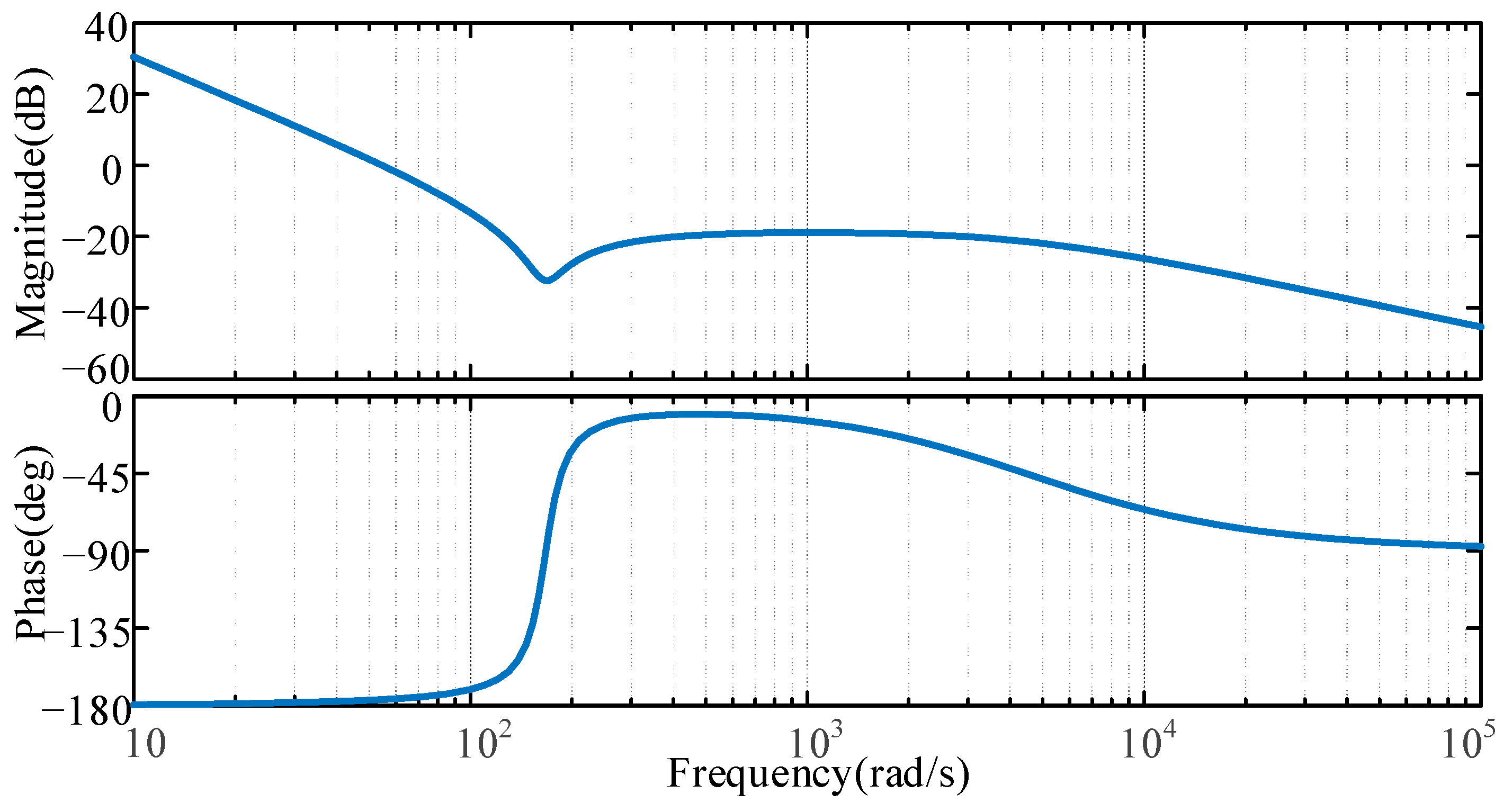
Bring the data in Table 2 into Equation (28), and the transfer function Gid(s) can be obtained.
G id s = s C V DC s 2 L C + s C R + n = 6 s 1.8 × 10 4 s 2 + 6 × 10 3 s + n
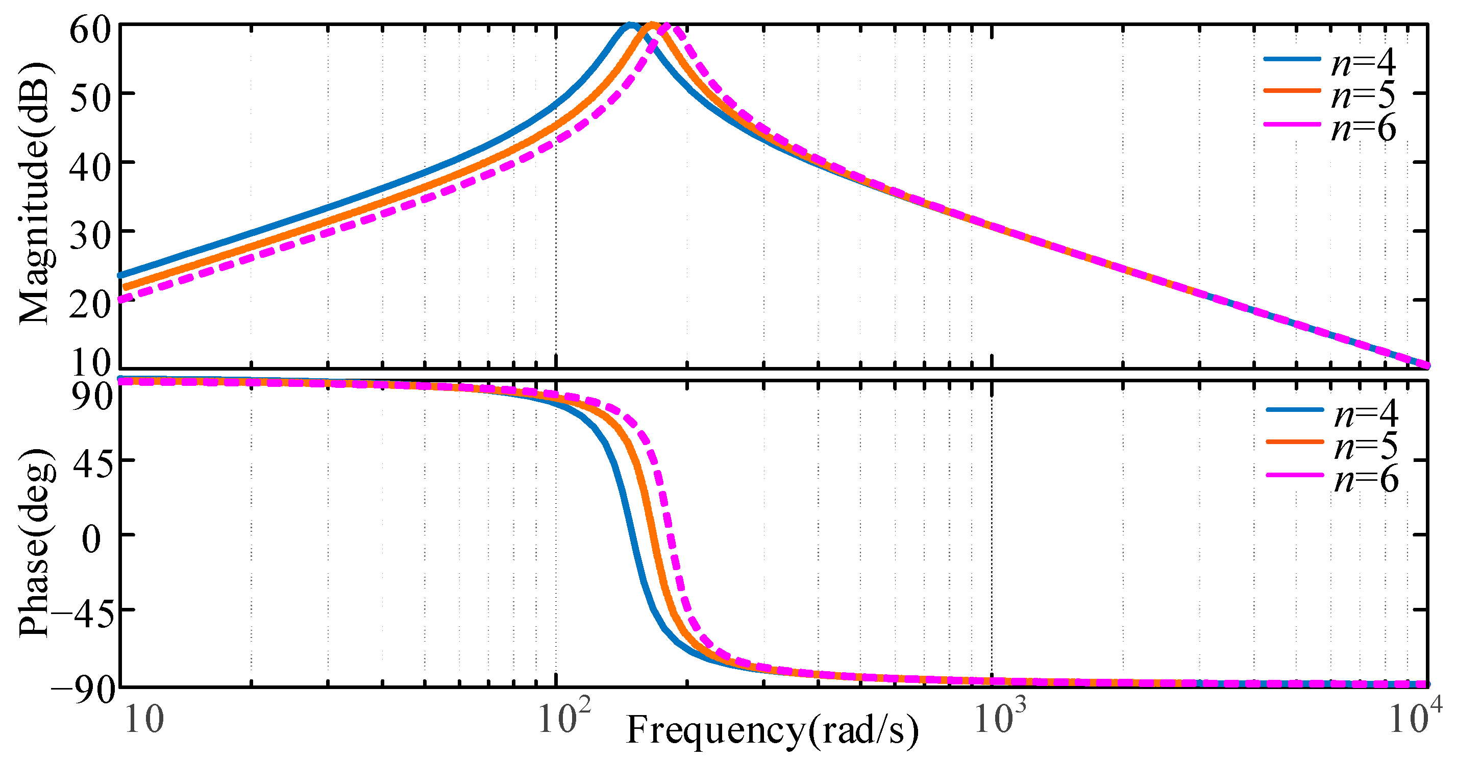
The Bode diagram corresponds to Gid(s) when the working multiples are 4, 5, and 6 respectively, as shown in Figure 9. It can be seen from the figure that the shapes of the Bode diagrams under different multiplicities are the same, so the transfer function of the five multiplicities is selected as the research object, and the current compensation network is designed.
As can be seen from Figure 9, the amplitude-frequency characteristic curve is rising in the low-frequency band, there is a large steady-state error in the system. In the middle-frequency band, the crossover frequency is very high, and the system may be affected by switching frequency, harmonics, parasitic oscillation, and so on, unable to work stably. The high-frequency band declines slowly, and the system is vulnerable to high-frequency noise [29].

4.2. The Design of the Current Compensation Network

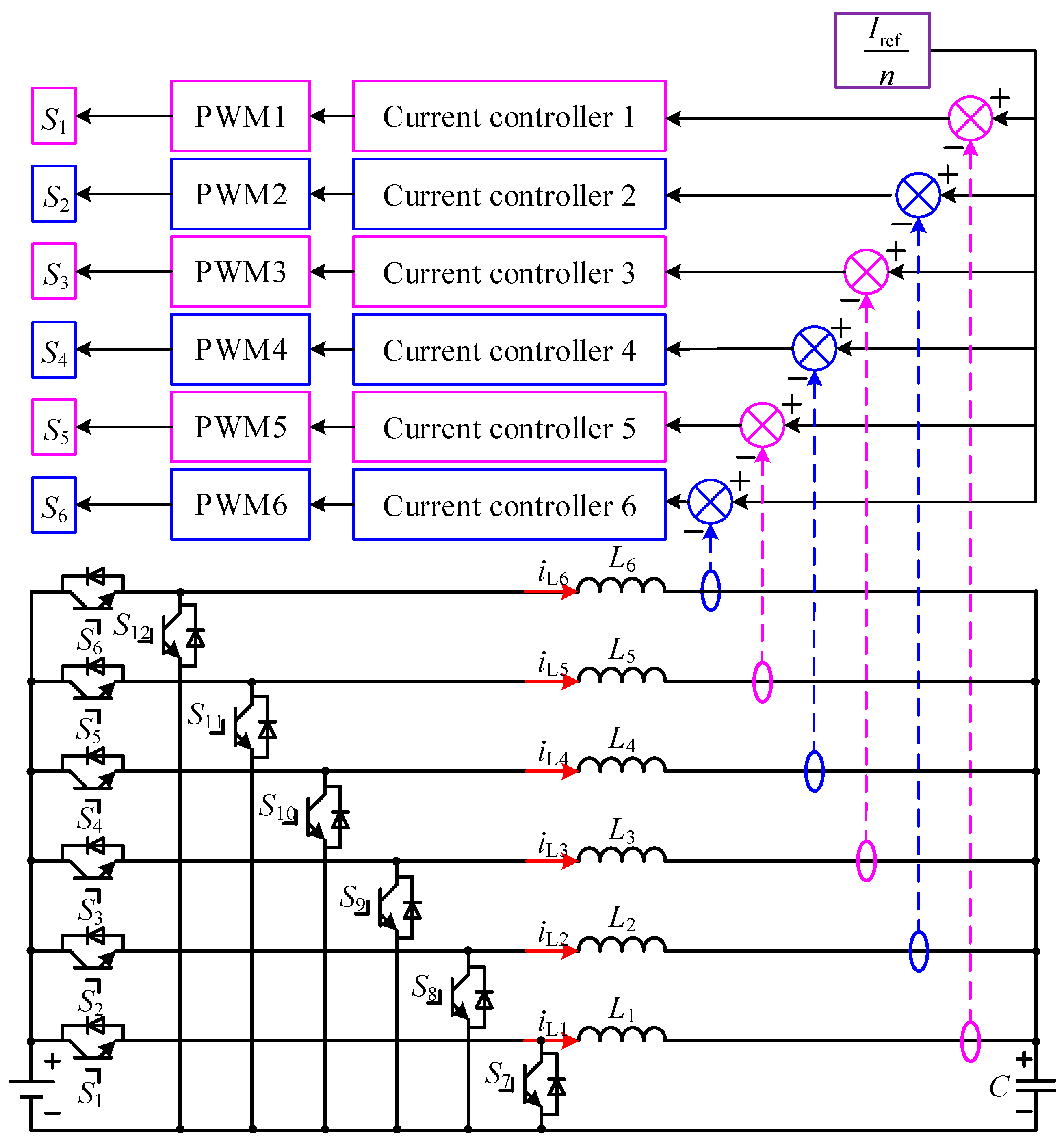
Due to the output current of variable multiplicity interleaving bidirectional DC/DC power converter being constant, the single current closed-loop control can be adopted, and the control strategy diagram is shown in Figure 10.
When the converter is operating in Buck mode, and the number of working multiplicities is 5, then the transfer function of the current-loop-controlled object can be shown as.
G id s = 6 s 1.8 × 10 4 s 2 + 6 × 10 3 s + 5
Through the analysis of the above Bode diagram, it can be seen that there are at least two integral links in the compensation link so that the amplitude-frequency characteristic curve can decrease at the slope of −20 dB/dec in the low-frequency band. In order to make the system have a strong ability to suppress high-frequency noise, the high-frequency band of the amplitude-frequency characteristic curve should decrease at the slope of 40 dB/dec [29].
The transfer function of the current compensation network is:
G idc s = K s + ω Z 1 s + ω Z 2 s 2 s + ω p
The aim of introducing two integral links into the above formula is to make the amplitude-frequency characteristic curve decrease at the slope of −20 dB/dec in the low-frequency band. ω Z 1 and ω Z 2 are introduced to offset the two conjugate poles in the original transfer function. The ωp can ensure that the corrected system has enough phase angle margin, at the same time, the amplitude-frequency characteristic curve can decrease at the slope of −40 dB/dec in the high-frequency band to suppress the high-frequency noise [29].
The transfer function of the current compensation link is:
G idc s = 3 × 10 6 × 1.8 × 10 4 s 2 + 6 × 10 3 s + 5 s 2 × s + 4500
The Bode diagram of the current compensation link is shown in Figure 11.
The open-loop transfer function of the corrected system is shown as.
G A s = G id s G idc s = 1.8 × 10 7 s s + 4500
The open-loop amplitude-frequency characteristic curve of the corrected system is shown in Figure 12. It can be seen from the figure that, after correction, the amplitude-frequency characteristic curve of the corrected system decreases at the slope of 20 dB/dec in the low-frequency band, and the steady-state error of the system is zero; The phase angle margin in the middle-frequency band is 54.2°, which meets the stability requirement. The crossing frequency is 3.24 × 10 3 rad / s ( f c 515.7 Hz ). The amplitude-frequency characteristic curve of the corrected system decreases at the slope of −40 dB/dec in the high-frequency band, and the system has a good ability to suppress the high-frequency noise. To sum up, the corrected system meets the design requirements.

4.3. The Simulation of the Variable Multiplicity Interleaving Bidirectional DC/DC Power Converter

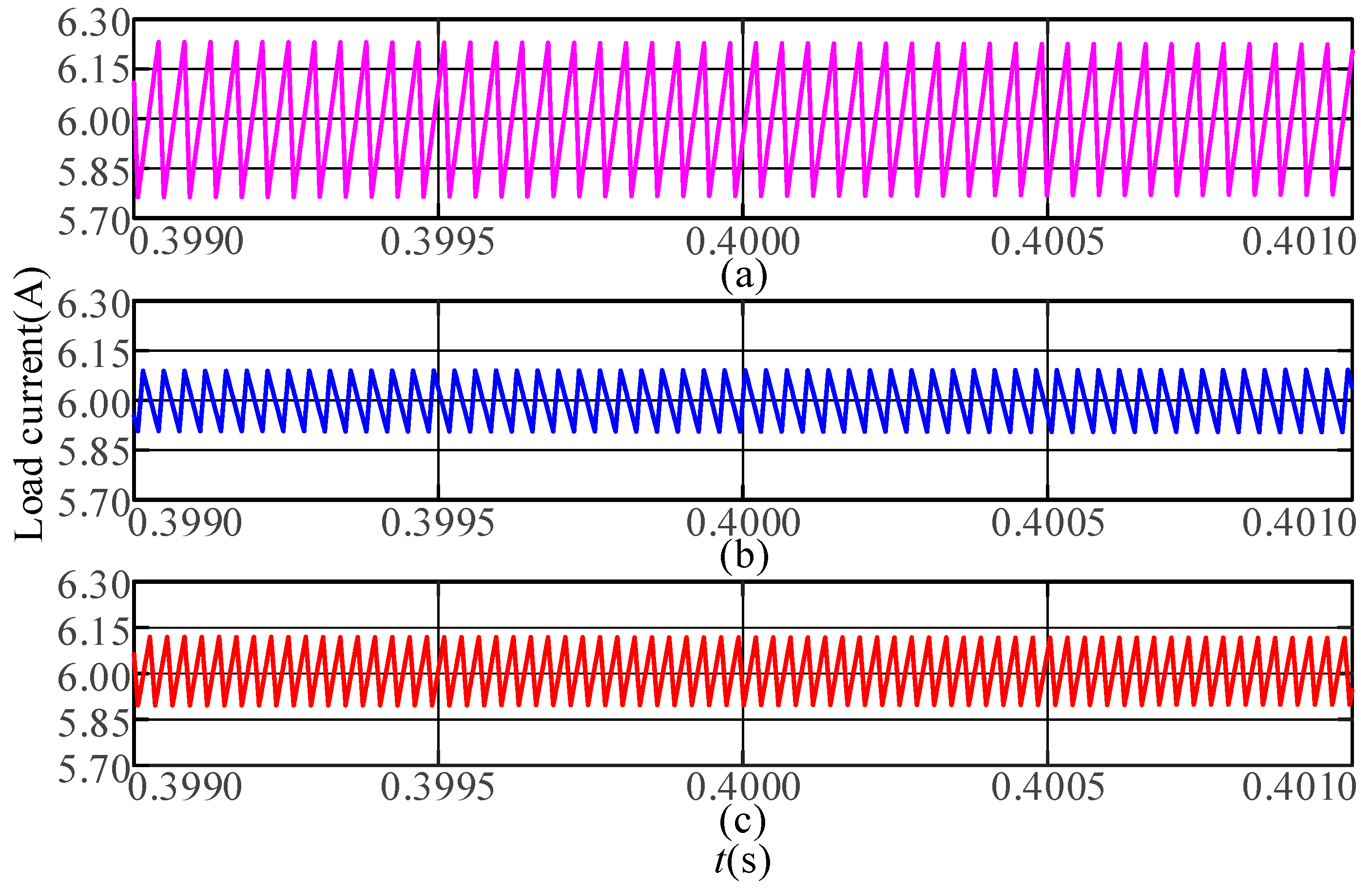
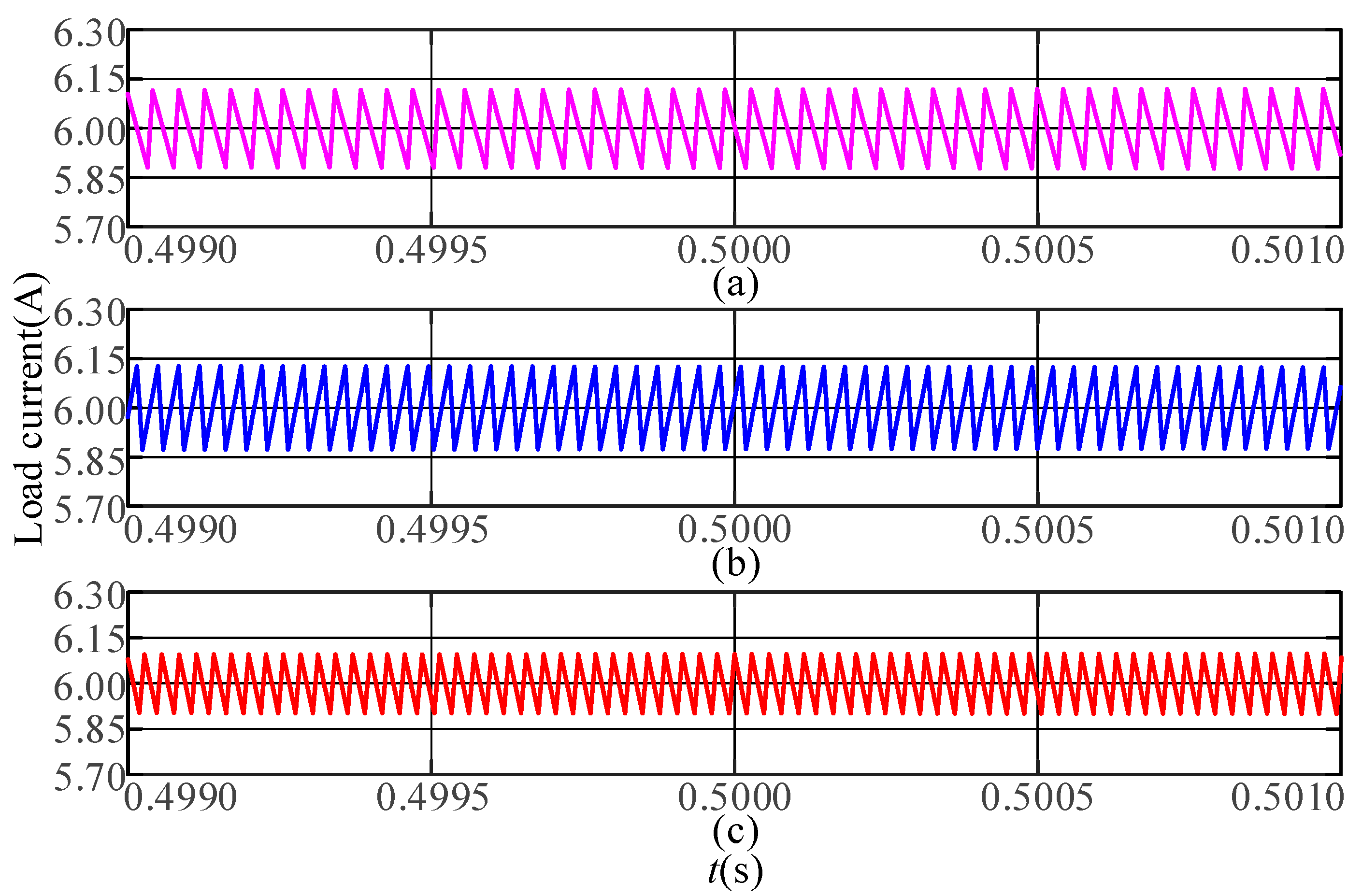
Based on the analysis of the previous chapters, the simulation model is built, and then the parameters in Table 2 are brought into the model. The simulation model is operated to extract the current ripples of different parallel numbers when the duty cycle is 0.25, 0.33, 0.40, and 0.5, which are shown in Figure 13, Figure 14, Figure 15 and Figure 16 (In each Figure, a is the current ripples in four parallel multiplicities; b is the current ripples in five parallel multiplicities; c is the current ripples in six parallel multiplicities.). Figure 13 shows the output current ripples when the duty cycle is 0.25, and the current ripple is the smallest when the parallel number is four; Figure 14 shows the output current ripples when the duty cycle is 0.33, and the current ripple is the smallest when the parallel number is six; Figure 15 shows the output current ripples when the duty cycle is 0.4, and the current ripple is the smallest when the parallel number is five; Figure 16 shows the output current ripples when the duty cycle is 0.50, and the current ripple is the smallest when the parallel number is six. The above simulation results are consistent with the conclusion in Table 1, which is obtained from the previous analysis, this is when the duty cycle is different, the number of parallel multiplicities with the smallest current ripples is different, and so the DC/DC converter needs to flexibly choose to turn on or turn off some parallel branches according to the current ripple optimization law.

5. The Experiment and Results

5.1. Experimental Platform

The experimental platform is shown in Figure 17, it can be divided into a control module, power module, output module, power supply, and programmable load. The TMS320F28377 microcontroller is used to control the whole system, and the XC3S500E-PQ208 is used to generate the PWM signal with the specific phase shift angle. The PWM signal is transmitted to the power module through the optical fiber. In the experiment, the 30 V bus voltage is generated by the DC stabilized power supply, the load capacitance C is replaced by a programmable load, the switching frequency is set to 10 KHz, the value of filter inductance is 3 mH, the output current is 6 A.

5.2. The Experimental Results of the Current Ripple Optimization in Variable Channel Interleaving Bidirectional DC/DC Power Converter

The current ripples of the 6 A output current of the DC-DC converter are shown in Figure 18. Figure 18a–l represents the current ripples which are corresponding to different multiplicities in parallel when the duty cycles are 0.25, 0.33, 0.4, and 0.5, respectively. As can be seen in Figure 18a–c, when the duty cycle is 0.25, the maximum current ripples are 80 mA, 100 mA, and 120 mA when the number of parallel multiplicities is 4, 5, and 6, respectively. As can be seen in Figure 18d–f, when the duty cycle is 0.33, the maximum current ripples are 160 mA, 145 mA, and 65 mA, when the number of parallel multiplicities is 4, 5, and 6, respectively. As can be seen in Figure 18g–y, when the duty cycle is 0.4, the maximum current ripples are 200 mA, 90 mA, and 100 mA, when the number of parallel multiplicities is 4, 5, and 6, respectively. As can be seen in Figure 18j–l, when the duty cycle is 0.5, the maximum current ripples are 130 mA, 140 mA, and 120 mA when the number of parallel multiplicities is 4, 5, and 6, respectively.
All optimization results of current ripples under different duty cycles and parallel multiplicities in Figure 18 are identical to not only the simulation results above but also the analytical results in Table 1, which demonstrate that the optimization method proposed in this paper is precise and practical.
The three pictures of the same line in Figure 18 clearly show the size of the current ripple under a different number of parallel channels with the same duty cycle. By extracting the data in Figure 18, Table 3 can be obtained. Compared with Figure 18, Table 3 is more intuitive and convincing in numerical representation. Table 3 intuitively illustrates the number of parallel branches that should be taken to minimize the current ripple under experimental conditions.
In order to simplify the analysis process, only the current ripples corresponding to duty cycles 0.25 and 0.5 are adopted. Figure 19a–f shows the current ripples of the first three channels when the parallel multiplicity is 4, 5, and 6. It can be seen that the larger the duty cycle, the longer the rise time and the shorter the fall time, the peak value of the ripple peak of a single brand is also increasing, and the total output current ripple is composed of multiple brand parallel outputs, so the total output current ripple cannot be judged only by the size of a single brand current ripple. The current of each channel is not completely coincident, mainly due to the measurement error of the sensor. Even if the current sharing control method is taken, the current imbalance caused by the inconsistent parameters of each channel cannot be fully compensated.

6. Conclusions

The main contribution of this paper is to propose a variable multiplicity control method of multiple interleaving bidirectional DC/DC power converters to optimize the current ripple, that is, dynamically adjust the number of parallel multiplicities in the actual operation of the circuit according to the duty cycles, so that the output current ripple is as small as possible. First, the relationship between the current ripple and the number of parallel multiplicities and the duty cycle is analyzed and deduced and the switching logic that can generate the minimum current ripple is designed. Second, the average value model and the AC small signal model of variable multiplicity interleaving bidirectional DC/DC power converter are established, and the transfer function of the system is obtained. Third, according to the transfer function of the system, the control system of the converter is designed. Simulation and experimental results show that the control method proposed in this paper can effectively further reduce the current ripple of the traditional multiple DC/DC converter, and to a certain, reduce the switching loss caused by a blind increase of switching frequency to optimize current ripple, so it is of great significance. All in all, the current ripple optimization algorithm proposed in this paper is suitable for occasions that require low current ripple, such as battery energy storage systems, electric vehicles, etc. However, due to multiple interleaving DC/DC converters using more parallel branches, the cost is relatively high. Further research on improving reliability and reducing costs is needed in the future.

Author Contributions

Conceptualization, J.D. and S.W.; methodology, S.F.; validation, Y.X.; formal analysis, K.Z. and L.S.; writing—original draft preparation, J.D., S.W. and Y.X.; writing—review and editing, J.D., S.W. and Y.X. All authors have read and agreed to the published version of the manuscript.

Funding

This research was funded by the National Natural Science Foundation of China, grant number 52177211, and by the Heilongjiang Postdoctoral Research Starting Fund, grant number LBH-Q20020.

Institutional Review Board Statement

Not applicable.

Informed Consent Statement

Not applicable.

Data Availability Statement

Not applicable.

Conflicts of Interest

The authors declare no conflict of interest.

References

  1. Hannan, M.A.; Wali, S.B.; Ker, P.J.; Abd Rahman, M.S.; Mansor, M.; Ramachandaramurthy, V.K.; Muttaqi, K.M.; Mahlia, T.M.I.; Dong, Z.Y. Battery energy-storage system: A review of technologies, optimization objectives, constraints, approaches, and outstanding issues. J. Energy Storage 2021, 42, 103–110. [Google Scholar] [CrossRef]
  2. Tong, Y.; Liang, J.; Liu, H.K.; Dou, S.X. Energy storage in Oceania. Energy Storage Mater. 2019, 20, 176–187. [Google Scholar] [CrossRef]
  3. Mahmoud, M.; Ramadan, M.; Olabi, A.G.; Pullen, K.; Naher, S. A review of mechanical energy storage systems combined with wind and solar applications. Energy Convers. Manag. 2020, 210, 112–125. [Google Scholar] [CrossRef]
  4. Babu, T.S.; Vasudevan, K.R.; Ramachandaramurthy, V.K.; Sani, S.B.; Chemud, S.; Lajim, R.M. A comprehensive review of hybrid energy storage systems: Converter topologies, control strategies and future prospects. IEEE Access 2020, 8, 148702–148721. [Google Scholar] [CrossRef]
  5. Lee, H.S.; Yun, J.J. High-efficiency bidirectional buck–boost converter for photovoltaic and energy storage systems in a smart grid. IEEE Trans. Power Electron. 2018, 34, 4316–4328. [Google Scholar] [CrossRef]
  6. Zhang, Y.; Cheng, X.F.; Yin, C.; Cheng, S. A soft-switching bidirectional DC–DC converter for the battery super-capacitor hybrid energy storage system. IEEE Trans. Ind. Electron. 2018, 65, 7856–7865. [Google Scholar] [CrossRef]
  7. Zhuo, S.; Gaillard, A.; Li, Q.; Ma, R.; Paire, D.; Gao, F. Current ripple optimization of four-phase floating interleaved DC–DC boost converter under switch fault. IEEE Trans. Ind. Appl. 2020, 56, 4214–4224. [Google Scholar] [CrossRef]
  8. Amiri, M.; Farzanehfard, H. A High-Efficiency Interleaved Ultra-High Step-Down DC–DC Converter with Very Low Output Current Ripple. IEEE Trans. Ind. Electron. 2018, 66, 5177–5185. [Google Scholar] [CrossRef]
  9. Nag, S.S.; Mishra, S.; Joshi, A. A passive filter building block for input or output current ripple cancellation in a power converter. IEEE J. Emerg. Sel. Top. Power Electron. 2015, 4, 564–575. [Google Scholar] [CrossRef]
  10. Wang, Z.; Wang, P.; Li, B.; Ma, X.; Wang, P. A Bidirectional DC–DC Converter with High Voltage Conversion Ratio and Zero Ripple Current for Battery Energy Storage System. IEEE Trans. Power Electron. 2020, 36, 8012–8027. [Google Scholar] [CrossRef]
  11. Villarreal-Hernandez, C.A.; Ruiz-Martinez, O.F.; Mayo-Maldonado, J.C.; Escobar, G.; Valdez-Resendiz, J.E.; Rosas-Caro, J.C. Minimum Current Ripple Point Tracking Control for Interleaved Dual Switched-Inductor DC–DC Converters. IEEE Trans. Ind. Electron. 2020, 68, 175–185. [Google Scholar] [CrossRef]
  12. Hu, X.; Ma, P.; Wang, J.; Tan, G. A hybrid cascaded DC–DC boost converter with ripple reduction and large conversion ratio. IEEE J. Emerg. Sel. Top. Power Electron. 2019, 8, 761–770. [Google Scholar] [CrossRef]
  13. Yuan, Z.; Xu, H. Pulse power supply with faster response and low ripple current using inductive storage and interleaving technology. CPSS Trans. Power Electron. Appl. 2020, 5, 54–62. [Google Scholar] [CrossRef]
  14. Lin, B.R.; Hsieh, F.Y.; Wang, D. Analysis, design and implementation of active clamp zero voltage switching converter with output ripple current cancellation. IEE Proc.-Electr. Power Appl. 2006, 153, 653–663. [Google Scholar] [CrossRef]
  15. Kumar, A.; Sensarma, P. Ripple-free input current high voltage gain DC–DC converters with coupled inductors. IEEE Trans. Power Electron. 2018, 34, 3418–3428. [Google Scholar] [CrossRef]
  16. Azer, P.; Emadi, A. Generalized state space average model for multi-phase interleaved buck, boost and buck-boost DC-DC converters: Transient, steady-state and switching dynamics. IEEE Access 2020, 8, 77735–77745. [Google Scholar] [CrossRef]
  17. Kanzian, M.; Agostinelli, M.; Huemer, M. Digital hysteresis sliding mode control for interleaved DC–DC converters. Control Eng. Pract. 2019, 90, 148–159. [Google Scholar] [CrossRef]
  18. Hu, R.; Yan, Z.; Wang, L.; Wong, M.C.; Zeng, J.; Liu, J.; Hu, B. An Interleaved Bidirectional Coupled-Inductor Based DC–DC Converter with High Conversion Ratio for Energy Storage System. IEEE Trans. Ind. Electron. 2021, 69, 5648–5659. [Google Scholar] [CrossRef]
  19. Alghaythi, M.L.; O’Connell, R.M.; Islam, N.E.; Khan, M.M.S.; Guerrero, J.M. A high step-up interleaved DC-DC converter with voltage multiplier and coupled inductors for renewable energy systems. IEEE Access 2020, 8, 123165–123174. [Google Scholar] [CrossRef]
  20. Ni, L.; Patterson, D.J.; Hudgins, J.L. High power current sensorless bidirectional 16-phase interleaved DC-DC converter for hybrid vehicle application. IEEE Trans. Power Electron. 2011, 27, 1141–1151. [Google Scholar] [CrossRef] [Green Version]
  21. Alzahrani, A.; Ferdowsi, M.; Shamsi, P. A family of scalable non-isolated interleaved DC-DC boost converters with voltage multiplier cells. IEEE Access 2019, 7, 11707–11721. [Google Scholar] [CrossRef]
  22. Kabalo, M.; Paire, D.; Blunier, B.; Bouquain, D.; Simoes, M.G.; Miraoui, A. Experimental validation of high-voltage-ratio low-input-current-ripple converters for hybrid fuel cell supercapacitor systems. IEEE Trans. Veh. Technol. 2012, 61, 3430–3440. [Google Scholar] [CrossRef]
  23. Mayer, R.; El Kattel, M.B.; Oliveira, S.V.G. Multiphase interleaved bidirectional DC/DC converter with coupled inductor for electrified-vehicle applications. IEEE Trans. Power Electron. 2020, 36, 2533–2547. [Google Scholar] [CrossRef]
  24. Yan, H.; Xu, Y.; Zou, J.; Wang, B.; Jiang, S. A maximum current sharing method for dual-redundancy brushless DC Motor control. In Proceedings of the 17th International Conference on Electrical Machines and Systems (ICEMS), Hangzhou, China, 22–25 October 2014; pp. 1057–1061. [Google Scholar] [CrossRef]
  25. Gu, L.; Li, P. Hybrid PWM Control of Bidirectional DC/DC Resonant Converter for Low-Current-Ripple and Wide-Voltage-Gain Application. In Proceedings of the 2020 IEEE Applied Power Electronics Conference and Exposition (APEC), New Orleans, LA, USA, 15–19 March 2020; pp. 2158–2162. [Google Scholar] [CrossRef]
  26. Chakraborty, S.; Hasan, M.M.; McGahan, P.; Tran, D.D.; Geury, T.; Davari, P.; Blaabjerg, F.; EI Baghdadi, M.; Hegazy, O. Real-life mission profile oriented lifetime estimation of a SiC interleaved bidirectional HV DC/DC converter for electric vehicle drivetrains. IEEE J. Emerg. Sel. Top. Power Electron. 2022, 10, 5142–5167. [Google Scholar] [CrossRef]
  27. Elserougi, A.; Abdelsalam, I.; Massoud, A.; Ahmed, S. A non-isolated hybrid-modular DC-DC converter for DC grids: Small-signal modeling and control. IEEE Access 2019, 7, 132459–132471. [Google Scholar] [CrossRef]
  28. Ayachit, A.; Kazimierczuk, M.K. Averaged small-signal model of PWM DC-DC converters in CCM including switching power loss. IEEE Trans. Circuits Syst. II Express Briefs 2018, 66, 262–266. [Google Scholar] [CrossRef]
  29. Alvarez-Ramirez, J.; Cervantes, I.; Espinosa-Perez, G.; Maya, P.; Morales, A. A stable design of PI control for DC-DC converters with an RHS zero. IEEE Trans. Circuits Syst. I Fundam. Theory Appl. 2001, 48, 103–106. [Google Scholar] [CrossRef]
Figure 1. Bidirectional DC/DC converter in Buck mode.
Applsci 13 01744 g001
Figure 2. Multiple inductor current and total current waveform.
Applsci 13 01744 g002
Figure 3. The relationship among kLm, D, and n of bidirectional DC/DC converter in Buck mode.
Applsci 13 01744 g003
Figure 4. Relationship between kLm and D with different parallel multiplicity.
Applsci 13 01744 g004
Figure 5. Parallel multiplicity corresponding to the minimum current ripple coefficient under different duty cycles.
Applsci 13 01744 g005
Figure 6. The topology of variable multiplicity bidirectional DC/DC power converter.
Applsci 13 01744 g006
Figure 7. The average value model of the variable multiplicity bidirectional DC/DC power converter in Buck mode.
Applsci 13 01744 g007
Figure 8. The AC small signal model of the variable multiplicity bidirectional DC/DC power converter in Buck mode.
Applsci 13 01744 g008
Figure 9. The Bode diagrams when the working number of the parallel multiplicity is 4, 5, or 6.
Applsci 13 01744 g009
Figure 10. Control strategy diagram of variable multiplicity interleaving bidirectional DC/DC power converter.
Applsci 13 01744 g010
Figure 11. The Bode diagram of the current compensation link.
Applsci 13 01744 g011
Figure 12. The Bode diagram of the corrected system.
Applsci 13 01744 g012
Figure 13. Output current ripples of DC-DC converter with 0.25 duty cycle under the 6A output current. (a) The current ripples in four parallel multiplicities; (b) The current ripples in five parallel multiplicities; (c) The current ripples in six parallel multiplicities.
Applsci 13 01744 g013
Figure 14. Output current ripples of DC-DC converter with 0.33 duty cycle under the 6A output current. (a) The current ripples in four parallel multiplicities; (b) The current ripples in five parallel multiplicities; (c) The current ripples in six parallel multiplicities.
Applsci 13 01744 g014
Figure 15. Output current ripples of DC-DC converter with 0.40 duty cycle under the 6A output current. (a) The current ripples in four parallel multiplicities; (b) The current ripples in five parallel multiplicities; (c) The current ripples in six parallel multiplicities.
Applsci 13 01744 g015
Figure 16. Output current ripples of DC-DC converter with 0.50 duty cycle under the 6A output current. (a) The current ripples in four parallel multiplicities; (b) The current ripples in five parallel multiplicities; (c) The current ripples in six parallel multiplicities.
Applsci 13 01744 g016
Figure 17. Experimental platform.
Applsci 13 01744 g017
Figure 18. Output current ripples of DC-DC converter with different duty cycles under the same output current. (ac) The current ripples of different parallel multiplicities when the duty cycle is 0.25; (df) The current ripples of different parallel multiplicities when the duty cycle is 0.33; (gy) The current ripples of different parallel multiplicities when the duty cycle is 0.4; (jl) The current ripples of different parallel multiplicities when the duty cycle is 0.5.
Applsci 13 01744 g018
Figure 19. Current ripples of the first three channels under partial duty cycle when the parallel multiplicity is 4, 5, and 6. (a,c,e) The current ripples of the first three channels with the duty cycle of 0.25 when the parallel multiplicity is 4, 5, and 6; (b,d,f) The current ripples of the first three channels with the duty cycle of 0.5 when the parallel multiplicity is 4, 5, and 6.
Applsci 13 01744 g019
Table 1. The number of parallel multiplicities corresponding to different duty cycles.
Range of Duty CyclesNumber of Parallel Multiplicities
0.1000~0.18356
0.1835~0.22545
0.2254~0.28874
0.2887~0.36756
0.3675~0.47725
0.4772~0.55286
0.5528~0.63245
0.6324~0.71136
0.7113~0.77464
0.7746~0.81655
0.8165~0.90006
Table 2. Parameters of variable multiplicity interleaving bidirectional DC/DC converter.
ParameterValue
DC voltage VDC30 V
Switching period TS0.0001 s (10 kHz)
Inductance L3 mH
Inductance resistance R0.1 Ω
Load capacitance C0.06 F
Initial voltage of load capacitor V C 0 5 V
Load current ILoad6 A
Maximum number of parallel channels N 6
Table 3. Output current ripples of DC-DC converter with different duty cycles under the same output current.
Duty CyclesThe Maximum Current Ripple of the Number of N Multiple Parallel Channels/mAThe Number of Parallel Channels to Be Used
N = 4N = 5N = 6
0.25801001204
0.33160145656
0.40200901005
0.501301401206
Disclaimer/Publisher’s Note: The statements, opinions and data contained in all publications are solely those of the individual author(s) and contributor(s) and not of MDPI and/or the editor(s). MDPI and/or the editor(s) disclaim responsibility for any injury to people or property resulting from any ideas, methods, instructions or products referred to in the content.