1. Introduction
The pipeline analog-to-digital converter ADC architecture is the most suitable for high-speed operations with medium-to-high resolution among various ADC architectures. However, because the analog-to-digital conversion of the pipeline ADC is performed in the analog domain, various errors generated from analog circuits, such as charge injection, finite gain error of an operational amplifier (op-amp), and capacitor mismatch error, must be suppressed to achieve high resolution. Most errors, except capacitor mismatch error, can be addressed owing to advances in circuit techniques and CMOS technologies [
1,
2,
3,
4,
5]. However, capacitor mismatch significantly depends on the CMOS technology and requires special calibration circuitry to minimize the linearity degradation of the ADC output.
The calibration of capacitor mismatch has been investigated for several decades, and numerous techniques have been reported [
3,
6,
7,
8,
9,
10,
11,
12,
13,
14,
15,
16,
17,
18,
19,
20,
21]. Calibration techniques can be categorized into two types: analog and digital. Digital calibration techniques [
6,
7,
8,
9,
10,
11,
12] move analog errors to the digital domain by utilizing different methods and digitally correcting them. However, they increase circuit complexity and power consumption. In contrast, analog calibration has a simpler circuit design compared with digital calibration [
3,
13,
14,
15,
16,
17,
18,
19,
20,
21]. The capacitor error averaging technique proposed in [
3,
16,
17] is an effective analog calibration technique. In this technique, calibration can be performed in the background, meaning normal operation is not hindered by calibration. However, additional clock phases are required to average the capacitor mismatch errors, thereby decreasing the operation speed of the ADC. Self-calibration is another effective analog calibration technique [
18,
19,
20,
21]. As suggested by the name, self-calibration utilizes the remaining pipeline stages to correct capacitor mismatch errors in the early pipeline stages, thereby eliminating the need for calibration circuitry and simplifying circuit implementation. Unlike the error-averaging technique, although the calibration is performed in the foreground, the capacitance does not drift or age over time, and the foreground calibration still functions effectively.
This study proposes another method to implement self-calibration. Without increasing the circuit complexity, the proposed calibration circuit re-utilizes the multiplying digital-to-analog converter (MDAC) in a pipeline stage to recursively amplify the capacitor mismatch error and then converts it into a digital code by the remaining pipeline stages. The digital error is subtracted from the ADC output.
The advantage of the proposed method is that it does not increase circuit complexity and not require additional clock phases, which makes it suitable for high-speed operation. However, it is a foreground method, which means the normal operation has to be stopped during calibration. Although it is known that capacitor mismatch does not change significantly over time, periodic calibration might be required depending on applications.
A 12-bit pipeline ADC that employs self-calibration is fabricated by utilizing a 0.18 µm standard CMOS process. After calibration, the measured differential nonlinearity (DNL) and integral nonlinearity (INL) increase from +0.82/−0.75 and +1.12/−1.79 to +0.45/−0.41 and +0.47/−0.91, respectively. The dynamic performance also improves significantly after calibration. At a sampling rate of 30 MS/s, the ADC achieves a spurious-free dynamic range (SFDR) and a signal-to-noise and distortion ratio (SNDR) of 84.1 dB and 68.9 dB, for an input frequency of 2.09 MHz, respectively. The power consumption of the ADC is 35 mW under a 1.8 V supply and the figure of merit (FOM) is 512 fJ/conversion step.
The remainder of this paper is organized as follows:
Section 2 presents the proposed MDAC for self-calibration and its operating principles.
Section 3 explains the implementation of the ADC that employs the proposed self-calibration technique. Finally, the measurement results and conclusions are presented in
Section 4 and
Section 5, respectively.
2. Proposed Self-Calibration Technique
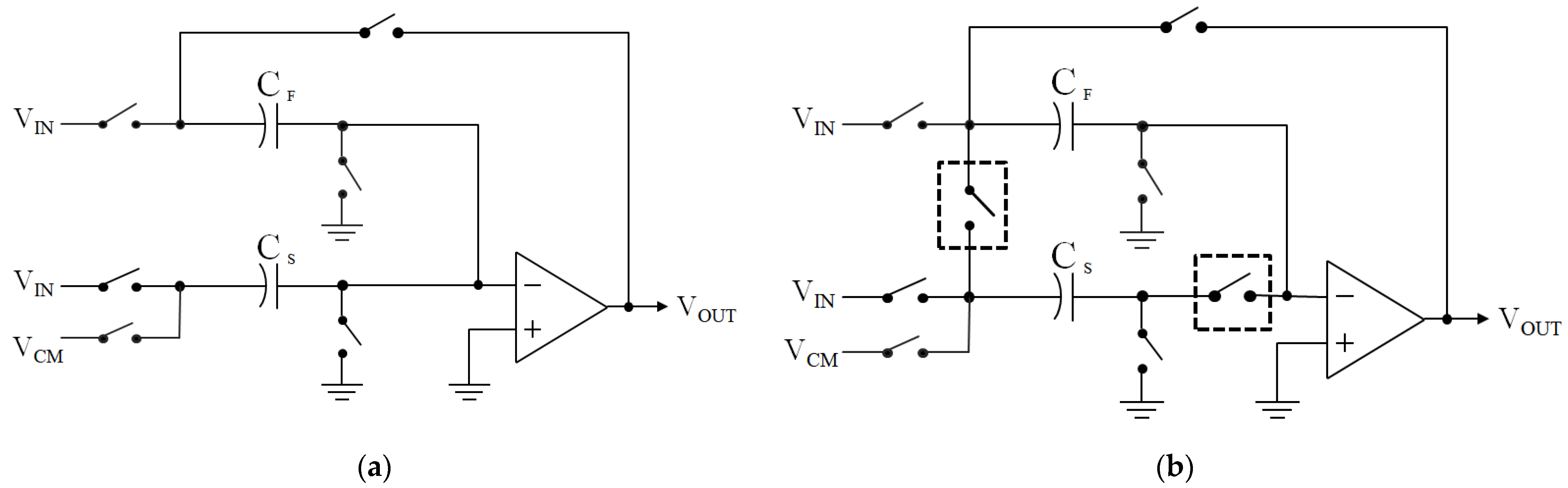
A switched-capacitor amplifier (SCA) with a gain of two is a key building block of the MDAC in a 1.5-bit pipeline stage. The conventional SCA and proposed self-calibrating SCA for gain-of-two amplification are shown in
Figure 1. Compared with the conventional SCA, only two additional switches, which are placed in the dashed box, are added to self-calibrate the capacitor mismatch error. Even though the calibration circuit is employed for the gain-of-two SCA for this work, it can be used for the SCA with various gains using a flip-around amplification scheme.
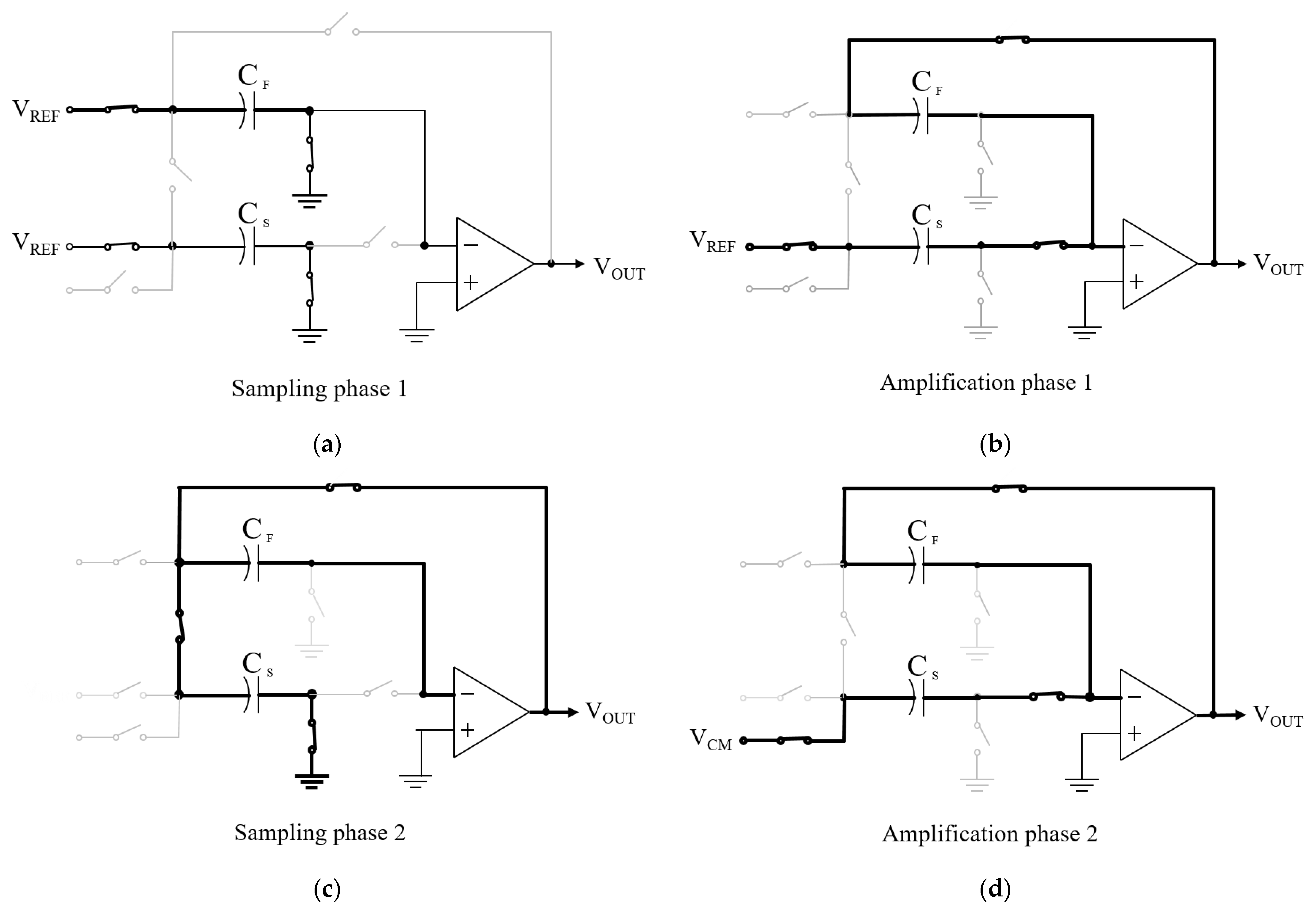
The SCA operates in two modes: calibration and normal. In calibration mode, the error voltage caused by the capacitor mismatch is converted into a digital signal, saved in memory, and subtracted from the ADC output. In normal operation, the two additional switches remain OFF and the SCA functions as a conventional MDAC for a 1.5-bit pipeline stage. The operation of the SCA during capacitor mismatch calibration is shown in
Figure 2. The SCA operates with a two-phase non-overlapping clock, sampling, and amplification phases, similar to the conventional SCA. In the sampling phase, the reference voltage V
REF is applied to the feedback capacitor (C
F) and a common-mode voltage or 0 is applied to the sampling capacitor (C
S), as shown in
Figure 2a. The total charge sampled on the capacitors is expressed as follows:
In the amplification phase, the bottom plate of C
F is flipped around and connected to the op-amp output, whereas the bottom plate of C
S is connected to V
REF, as shown in
Figure 2b. From the principle of charge conservation, the total charge Q at the end of the amplification phase is as follows:
Suppose C
F = C and C
S = (1 + ε)C. In that case, the op-amp output voltage becomes V
REF multiplied by the mismatch factor, which is called the error voltage (V
E), expressed as follows:
In sampling phase 2, as shown in
Figure 2c, V
OUT is sampled on C
S by turning S
4 and S6 ON. The charge on C
S is then transferred to C
F in amplification phase 2 and V
OUT becomes:
Since V
REF is known, the mismatch factor ε can be derived from the digitized value of V
E, converted by the remaining pipeline stages.
The proposed SCA is particularly advantageous in that VE can be accurately amplified by a power of two with no additional circuits by repeating the processes of sampling phase 2 and amplification phase 2.
Furthermore, amplification by a gain of two can be considered as a 1.5-bit pipeline stage operation when the amplitude input is relatively small. A block diagram of the 1.5-bit pipeline stage and its transfer curve for the stage’s analog input and output voltages are shown in
Figure 3, according to which the digital output is “01” and the MDAC output is twice the input when the input amplitude is within ±V
REF/4. Generally, the capacitor mismatch is small, and V
E remains within ±V
REF/4 even after several amplifications. Therefore, suppose the digital output is “01” even with no sub-ADC. In that case, the 1.5-bit stage operation is performed whenever V
E is amplified by a fact of two.
For self-calibration, redundant stages are required to accurately measure the mismatch errors generated by the front pipeline stages. For example, suppose the capacitor mismatch error that occurs in the first stage is converted to the remaining stages in a 12-bit pipeline ADC that performs a 1-bit or 1.5-bit conversion per stage. In that case, the converted error voltage has only 11-bit accuracy, which is insufficient for correction. At least two redundant stages must be added to increase the accuracy by more than two bits. As previously explained, amplification of the small-error voltage by a factor of two corresponds to the addition of one redundant stage. In other words, the accuracy of the error voltage is increased to 13 bits by amplifying the error voltage twice before it is converted by the remaining stages, which allows self-calibration with no additional circuitry. Calibration must only be performed for a few MSB stages according to the capacitor-matching characteristics provided in the CMOS process and proceeds in the reverse direction from the rear stage.
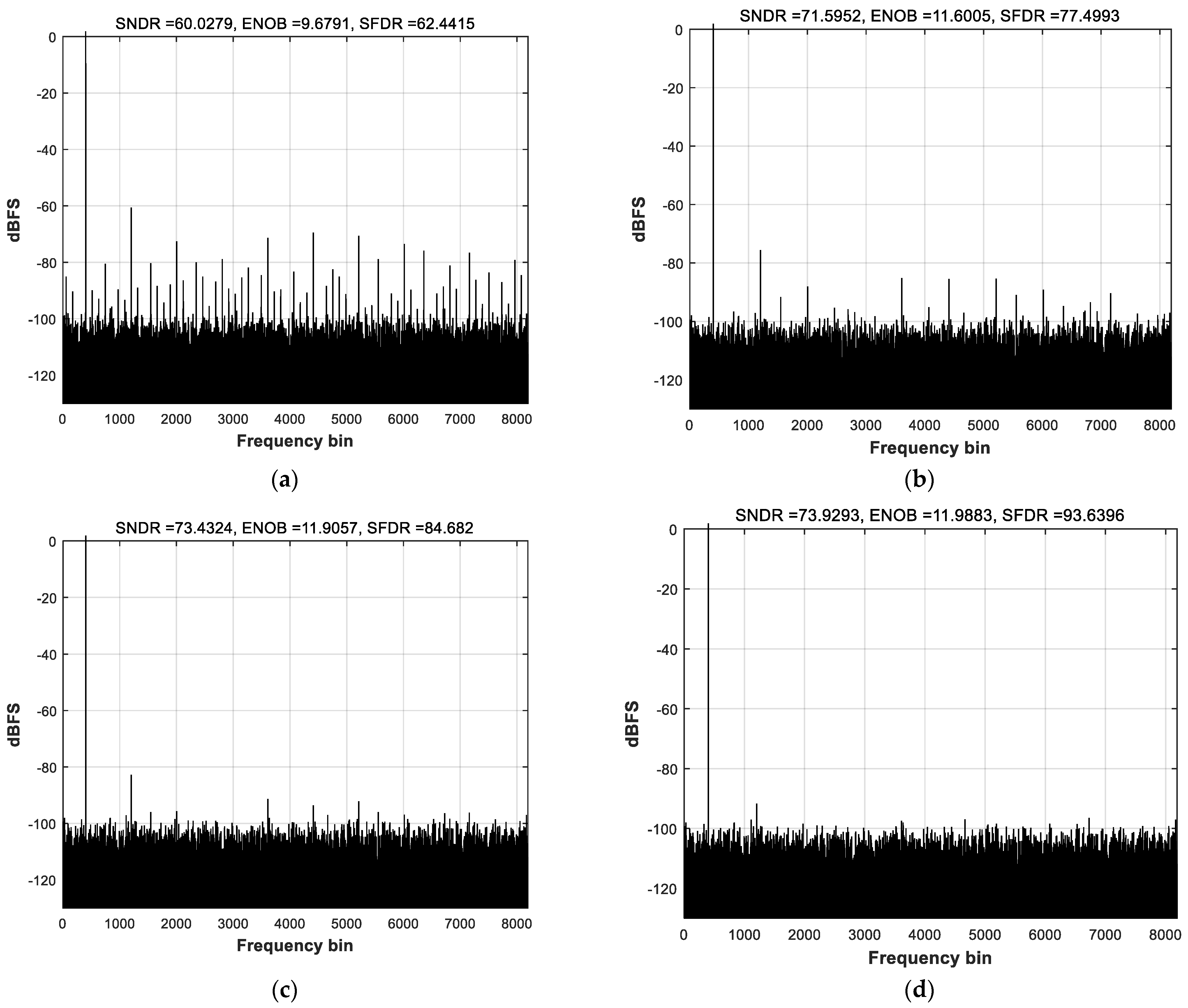
A comparison of the dynamic performance of a 12-bit pipeline ADC before and after calibration is shown in
Figure 4. In the simulations, only capacitor mismatch was considered, and calibration was performed for the first two stages. The mismatch between C
S and C
F was assumed to be 0.5% (ε is 0.005) based on the technology information. As shown in the simulation results, the mismatch calibration effectively improved the ADC performance. SNDR and SFDR increased from 59.9 dB to 73.9 dB and 62.3 dB to 93.6 dB, respectively. The dynamic performances were also compared according to the number of redundant bits or stages. As shown in
Figure 5, the performance improved with the number of redundant bits and saturated at 2 or more bits. Therefore, in this study, the number of redundant bits was determined to be two.
3. ADC Implementation
A 12-bit pipeline ADC was designed as the readout circuit in a CMOS image sensor.
Since the pixel output behaves like a DC signal and sample-to-sample conversion of the pixel signal is performed by the ADC, a static performance, especially differential nonlinearity, is more important than a dynamic performance and capacitor mismatch calibration is needed for this purpose.
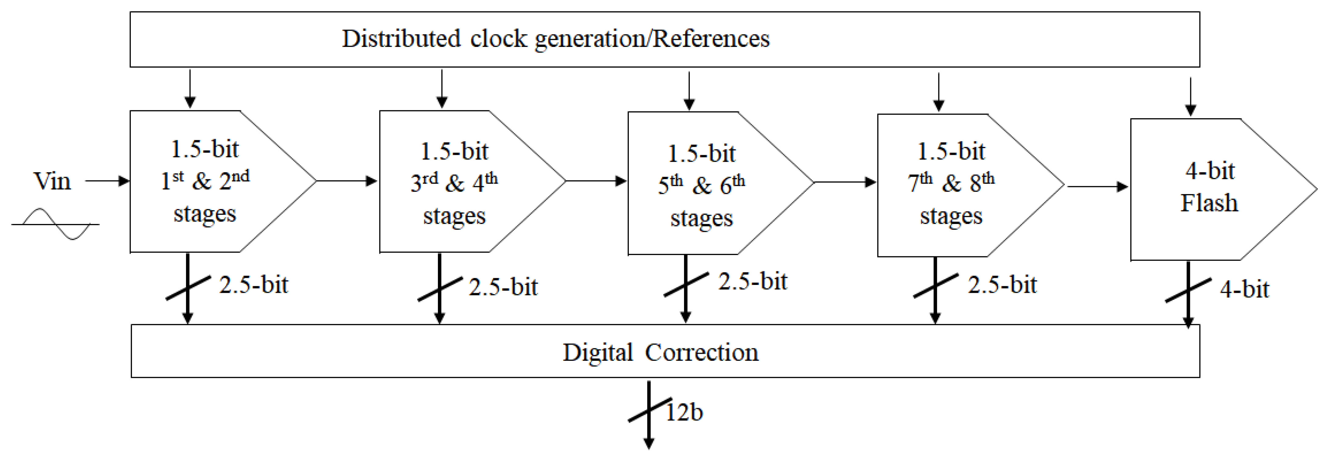
A block diagram of the ADC is shown in
Figure 6. The ADC was composed of eight 1.5-bit stages followed by a 4-bit flash ADC as the final stage, a reference generation circuit, and distributed clock drivers. A simplified circuit for the first stage is shown in
Figure 7. Because the ADC did not have a dedicated front-end sample or hold amplifier, the sub-ADC of the first stage had its own input sampling network that held the input signal while the comparator made its decision. The second stage was similar to the first and was a scaled-down version of the first stage, except that the sub-ADC did not have a sampling network. Capacitor mismatch calibration was performed only for the first and second stages. Therefore, from the 3rd stage, the circuit configurations were similar to that of the conventional 1.5-bit pipeline stage. An op-amp of the MDAC was shared between two adjacent stages to reduce power consumption [
22]. During calibration, the mismatch error between each C
S and C
F was amplified and converted into a digital signal, as explained in the previous section. During normal operation, the ADC output code was corrected by adding or subtracting the converted error voltage whenever the digital output value of the calibrated stage was either “00” or “10”.
A simplified circuit of the op-amp with a gain-boosting amplifier is shown in
Figure 8. A folded-cascode architecture with PMOS input transistors was employed to set the input common-mode (CM) voltage lower than the output CM voltage, and the output cascade transistors were gain-boosted to increase the DC gain of the op-amp without reducing the output signal swing. The switched-capacitor CM feedback circuit proposed in [
23] was utilized to determine the output CM voltage of the op-amp. As shown in
Figure 8, a simple differential pair was utilized as the gain-boosting amplifier. A PMOS transistor (M3) was added between the input transistors for CM control of the amplifier. The simulated DC gain of the op-amp was higher than 90 dB for all the corners.
Bandwidth of the op-amp was derived from the first order approximation of the amplifier transfer function. During the amplification phase, the op-amp is placed in feedback with a feedback factor (ß) of 1/2, and the op-amp output voltage in the first MDAC needs to settle within a half LSB voltage for 11-bit resolution. This requires a settling time of 7.6 times time constant (τ), which should be smaller than a half clock cycle, i.e., 16.7 ns. The resulting τ is about 2.2 ns and the unity-gain bandwidth of the op-amp, which is calculated as 1/(2π·ß·τ), is about 145 MHz. However, considering the static error caused by the finite op-amp gain and slewing of the op-amp, the actual unity-gain bandwidth was set to be about 250 MHz through transient simulations.
The op-amp for the first and second stages consumed approximately 4 mA from the 2.8 V supply. The second, third, and fourth op-amps consumed approximately 1 mA, 0.5 mA, and 0.5 mA, respectively.
A MOS transmission gate is used as a switch in the MDAC except for the switches that are connected to the common-mode voltages. They are implemented with only NMOS transistors. The switch size is determined based on the RC delay requirement. With a sampling frequency of 30 MHz, the required settling time for 12-bit resolution is about 8.3τ and this should be smaller than 16.7 ns. The resulting τ is about 2 ns. Since the sampling capacitance for the first MDAC is 0.8 pF, the switch on resistance is calculated to be 2.5 Kohm and the transistor size is chosen to meet this value. The input signal sampling is the most important because this often limits the ADC linearity. A bottom-plate sampling scheme similar to the one used in [
22] is also adopted to reduce the detrimental effect of signal-dependent charge injection from the sampling switches, and this significantly improves the ADC linearity. The simulated SFDR was greater than 90 dB, which is sufficient for the target linearity performance.
4. Measurement Results
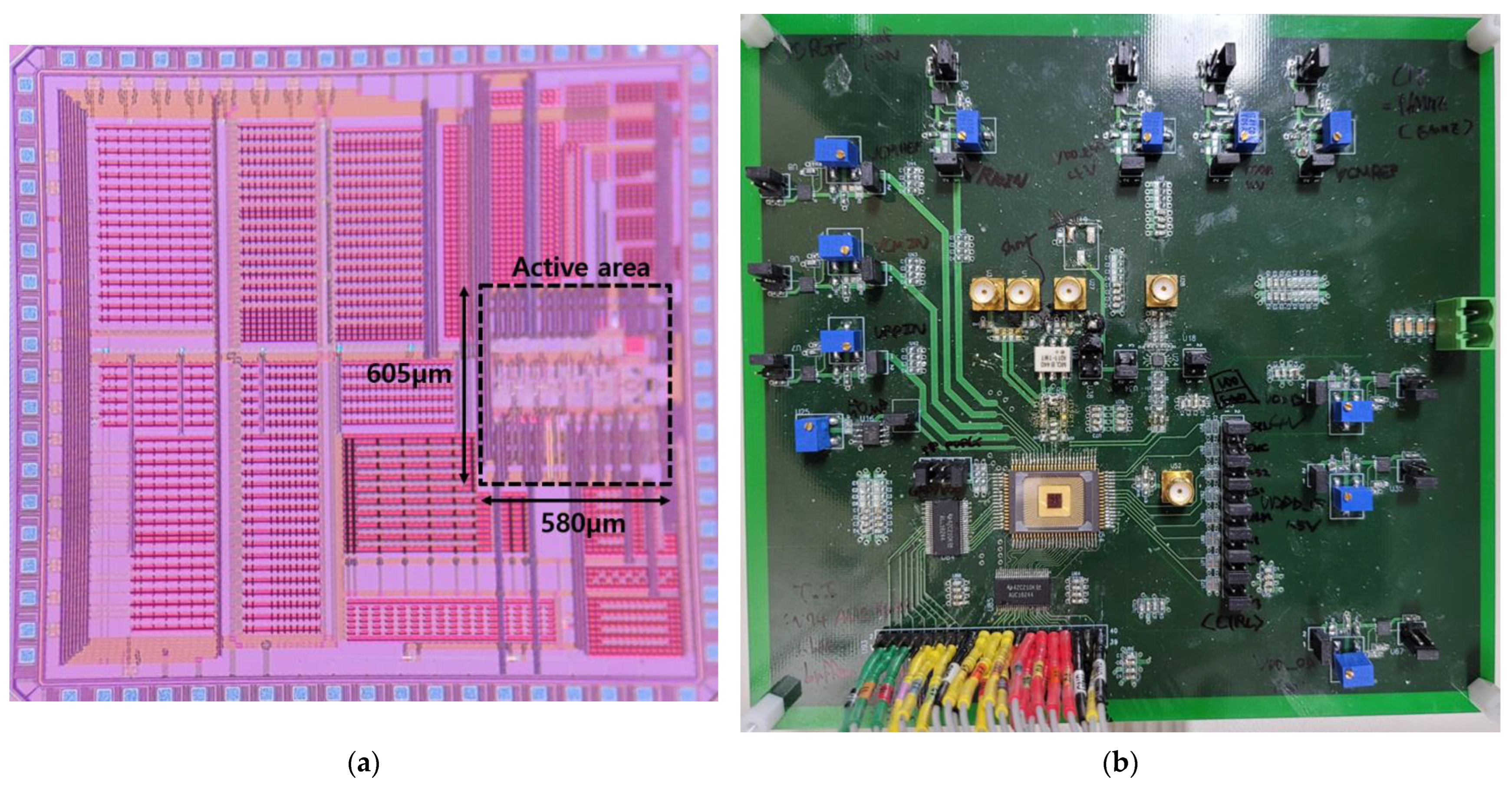
A 30 MS/s 12-bit pipeline ADC that employed the proposed self-calibrating technique was implemented in 0.18 µm CMOS technology and the ADC occupied a die area of 0.35 mm
2. The die micrograph and the printed circuit board for the chip measurement are shown in
Figure 9 and
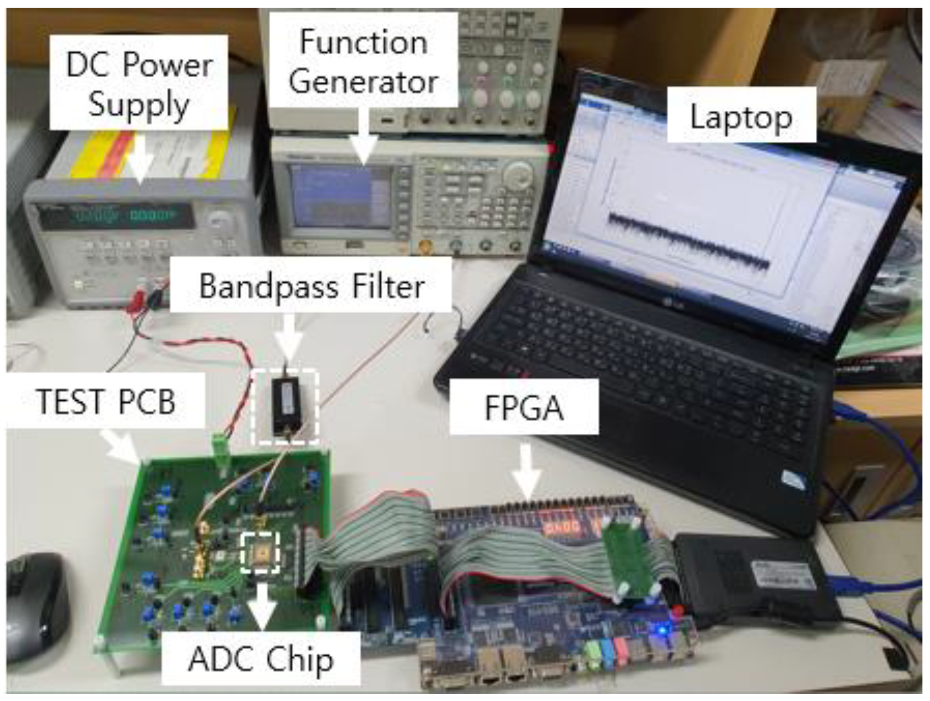
Figure 10 shows the measurement setup of the ADC. A single-ended sinusoidal signal is generated using a function generator and band-pass filtered for the purpose of anti-aliasing. The filtered single-ended signal is then converted to differential signals by using a transformer chip before it is applied to the ADC. The ADC output is captured by using a field programmable gate array (FPGA) board and transferred to a computer for performance evaluation.
The measured static performances of the ADC before and after calibration are shown in
Figure 11. Before the calibration, the measured DNL and INL were less than +0.82/−0.75 and +1.12/−1.79 LSB, respectively. After calibration, the DNL and INL improved to +0.45/−0.41 and +0.47/−0.91 LSB, respectively. The measured power spectra for input frequencies of 2.09 MHz and 14.1 MHz are also shown in
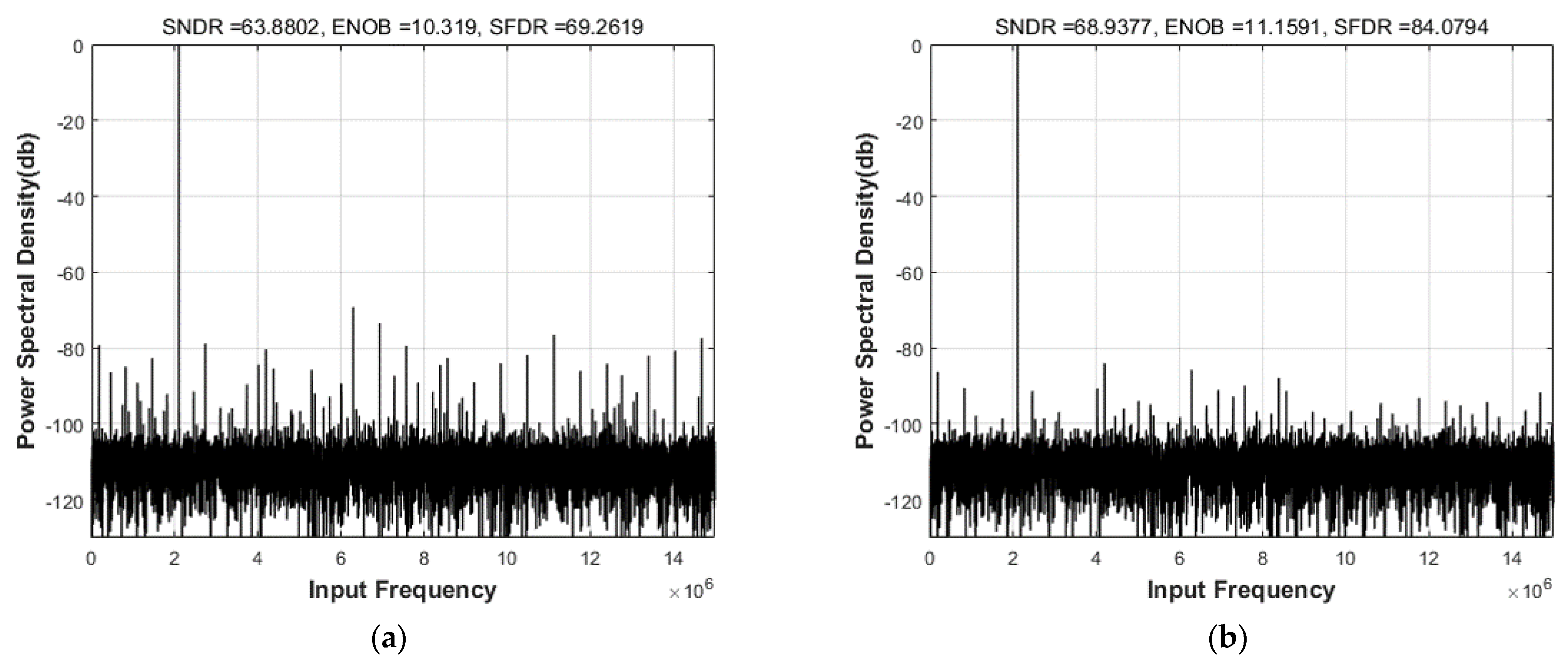
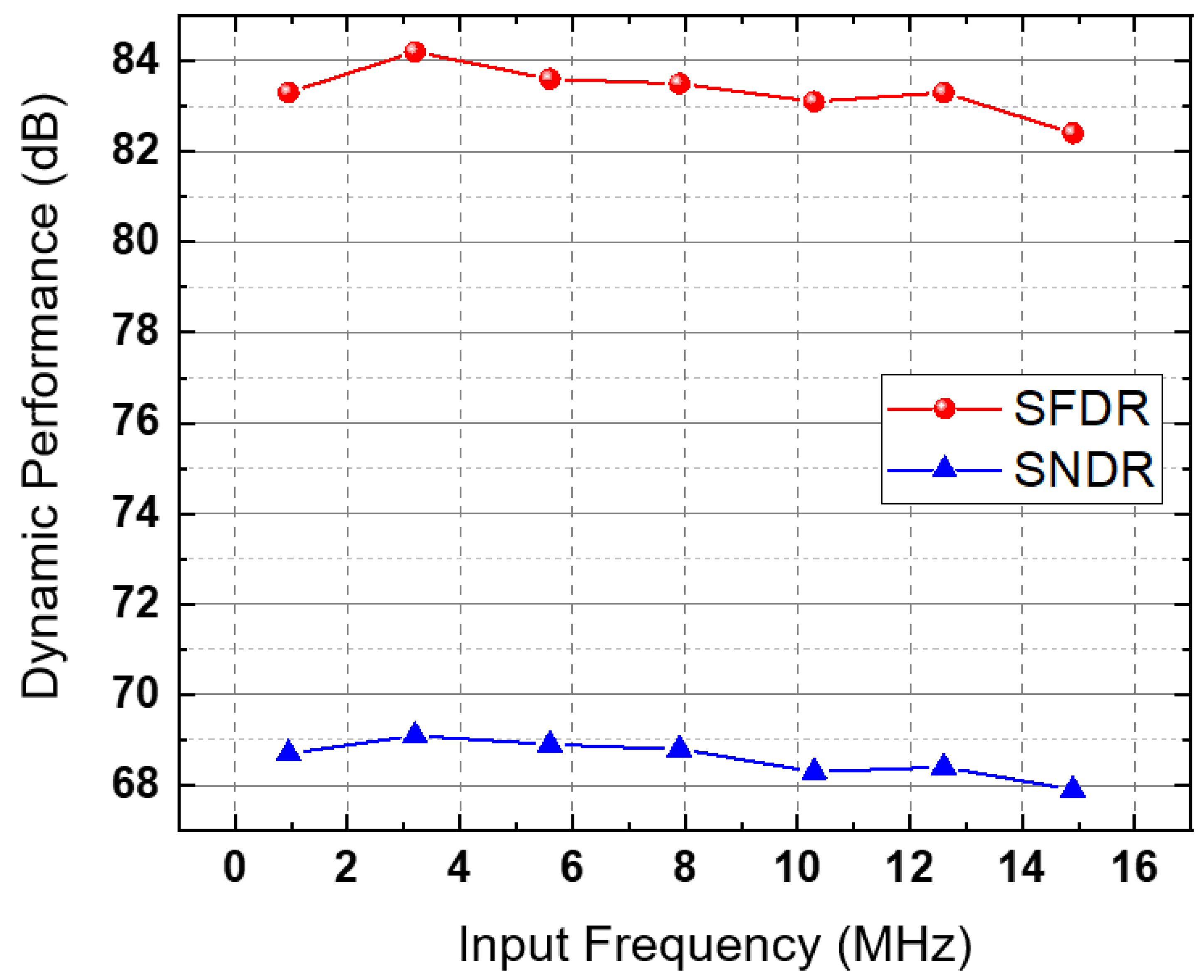
Figure 12, respectively. At an input frequency of 2.09 MHz, the measured SNDR and SFDR improved from 63.9 dB and 69.3 dB to 68.9 dB and 84.1 dB, respectively, and the resulting ENOB, calculated as (SNDR−1.76)/6.02, was 11.1 bit after calibration. After calibration, the measured dynamic performances versus the input frequency are shown in
Figure 13. The measured SNDR and SFDR varied from 67.9 to 69.1 dB, 82.4 to 84.2 dB, respectively, for input frequencies up to the Nyquist frequency. The total ADC power consumption was 35 mW, including the reference generation and all peripheral circuits. The FOM, which is calculated as power/(2
ENOB·sampling frequency), was 512 fJ/conversion. The ADC performance is summarized in
Table 1.
5. Conclusions
A simple yet effective self-calibration method was presented and verified through simulations and measurements. It was shown that the capacitor mismatch error can be minimized by adding a couple of switches to the conventional SCA and reusing the rest of the pipeline stages. A detailed explanation on the design of the main circuits in the MDAC was also presented. In order to minimize the finite-gain error of the op-amp, a gain-boosting amplifier was adopted in the op-amp and the detailed circuit diagram was presented. The resulting DC gain of the op-amp was more than 90 dB for all corner conditions. The settling behavior of the op-amp in the SCA was analyzed and the required time constant to achieve the target resolution was derived from the first-order approximation of the SCA transfer function. The bandwidth of the op-amp was then determined based on the analysis and optimized by using transient simulations. The effect of MOS switches on the input sampling and design of the sampling switch were also presented. A 12-bit 30 MS/s pipeline ADC comprising eight 1.5-bit stages, followed by a 4-bit flash ADC, was fabricated in a 180 nm CMOS process. After calibration, the measured DNL and INL improved from +0.82/−0.75 and +1.12/−1.79 to +0.45/−0.41 and +0.47/−0.91, respectively. Furthermore, calibration significantly improved the dynamic performance. For an input frequency of 2.09 MHz, the measured SFDR and SNDR improved from 69.3 dB and 63.9 dB to 84.1 dB and 68.9 dB, respectively, resulting in an ENOB of 11.1 bits. The ADC consumed 35 mW from an 1.8 V supply, and the resulting FOM was 512 fJ/conversion stage. Further improvement of the ADC linearity and power efficiency can be made by employing multi-bit per stage architectures such as 2.5-bit, 3.5-bit, etc. This can relax the settling requirement for the op-amp and capacitor mismatch error in the front stages.
Author Contributions
Conceptualization, D.-H.S.; methodology, D.-H.S. and J.-G.K.; validation, D.-H.S.; formal analysis, D.-H.S. and S.C.; writing—original draft preparation, D.-H.S. and S.C.; writing—review and editing, B.-G.L.; supervision, B.-G.L. All authors have read and agreed to the published version of the manuscript.
Funding
This work was supported in part by the National Research Foundation of Korea (NRF) Grant through the Korean Government (MSIT) under Grant 2021R1A2C22013480, and in part by the National Research and Development Program through the National Research Foundation of Korea (NRF) funded by the Ministry of Science and ICT under Grant NRF-2022M3H4A1A01009658.
Institutional Review Board Statement
Not applicable.
Informed Consent Statement
Not applicable.
Data Availability Statement
The data presented in this study are available on request from the corresponding author. The data are not publicly available due to nondisclosure agreement of the supporting project.
Conflicts of Interest
The authors declare no conflict of interest.
References
- Bult, K.; Geelen, G. A fast-settling CMOS opamp for SC circuits with 90-dB DC gain. IEEE J. Solid-State Circuits 1990, 25, 1379–1384. [Google Scholar] [CrossRef]
- Lewis, S.H.; Gray, P.R. A pipelined 5-Msample/s 9-bit analog-to-digital converter. IEEE J. Solid-State Circuits 1987, 22, 954–961. [Google Scholar] [CrossRef]
- Hung, T.-C.; Kuo, T.-H. A 75.3-dB SNDR 24-MS/s Ring Amplifier-Based Pipelined ADC Using Averaging Correlated Level Shifting and Reference Swapping for Reducing Errors from Finite Opamp Gain and Capacitor Mismatch. IEEE J. Solid-State Circuits 2019, 54, 1425–1435. [Google Scholar] [CrossRef]
- Stoeble, O.; Dias, V.; Schwoerer, C. An 80 MHz 10 b pipeline ADC with dynamic range doubling and dynamic reference selection. In Proceedings of the 2004 IEEE International Solid-State Circuits Conference, San Francisco, CA, USA, 15–19 February 2004; pp. 462–539. [Google Scholar]
- Lee, B.-G.; Min, B.-M.; Manganaro, G.; Valvano, J.W. A 14-b 100-MS/s Pipelined ADC With a Merged SHA and First MDAC. IEEE J. Solid-State Circuits 2008, 43, 2613–2619. [Google Scholar] [CrossRef]
- Moon, U.-K.; Song, B.-S. Background Digital Calibration Techniques for Pipelined ADC’s. IEEE J. Solid-State Circuits 1997, 44, 102–109. [Google Scholar]
- Guo, J.; Law, W.; Helms, W.J.; Allstot, D.J. Digital Calibration for Monotonic Pipelined A/D Converters. IEEE Trans. Instrum. Meas. 2004, 53, 1485–1492. [Google Scholar] [CrossRef]
- Furuta, M.; Kawahito, S.; Miyazaki, D. A Digital-Calibration Technique for Redundant Radix-4 Pipelined Analog-to-Digital Converters. IEEE Trans. Instrum. Meas. 2007, 56, 2301–2311. [Google Scholar] [CrossRef]
- Taherzadeh-Sani, M.; Hamoui, A. Digital Background Calibration of Capacitor-Mismatch Errors in Pipelined ADCs. IEEE Trans. Circuits Syst. II 2006, 53, 966–970. [Google Scholar] [CrossRef]
- Ragab, K.; Chen, L.; Sanyal, A.; Sun, N. Digital Background Calibration for Pipelined ADCs Based on Comparator Decision Time Quantization. IEEE Trans. Circuits Syst. II 2015, 62, 456–460. [Google Scholar] [CrossRef]
- Yang, Y.; Lyu, Y.; Hu, Y. A Mismatch Compensation Scheme for Cyclic-pipelined ADC via Dynamic Element Matching Technique. In Proceedings of the 2022 IEEE International Symposium on Circuits and Systems (ISCAS), Austin, TX, USA, 27 May–1 June 2022; pp. 3229–3233. [Google Scholar]
- Wei, J.; Zhang, C.; Liu, M. A 11-Bit 1-GS/s 14.9 mW Hybrid Voltage-Time Pipelined ADC With Gain Error Calibration. IEEE Trans. Circuits Syst. II Express Briefs 2022, 69, 799–803. [Google Scholar]
- Zhang, Y.; Zhang, J.; Liu, S.; Ding, R.; Zhu, Y.; Chan, C.-H.; Martins, R.P. A 20 MHz Bandwidth 79 dB SNDR SAR-Assisted Noise-Shaping Pipeline ADC With Gain and Offset Calibrations. IEEE J. Solid-State Circuits 2022, 57, 745–756. [Google Scholar] [CrossRef]
- Li, P.W.; Chin, M.J.; Gray, P.R.; Castello, R. A Ratio–Independent Algorithmic Analog-to-Digital Conversion Technique. IEEE J. Solid-State Circuits 1984, 19, 828–836. [Google Scholar] [CrossRef]
- Liu, H.; Sun, J.; Xu, H.; Zhang, L. A 16b 120 MS/s Pipelined ADC Using an Auxiliary-Capacitor-Based Calibration Technique Achieving 90.5 dB SFDR in 0.18 μm CMOS. IEEE Trans. Circuits Syst. II Express Briefs 2022, 69, 809–813. [Google Scholar] [CrossRef]
- Song, B.-S.; Tompsett, M.F.; Lakshmikumar, K.R. A 12-bit 1-Msample/s capacitor error-averaging pipelined A/D converter. IEEE J. Solid-State Circuits 1988, 23, 1324–1333. [Google Scholar] [CrossRef]
- Chen, H.-S.; Song, B.-S.; Bacrania, K. A 14-bit 20-Msample/s CMOS pipelined ADC. IEEE J. Solid-State Circuits 2001, 36, 997–1001. [Google Scholar] [CrossRef]
- Lee, H.-S.; Hodges, D.; Gray, P.R. A self-calibrating 12b 12s CMOS ADC. In Proceedings of the 1984 IEEE International Solid-State Circuits Conference. Digest of Technical Papers, San Francisco, CA, USA, 22–24 February 1984; pp. 64–66. [Google Scholar]
- Lin, Y.M.; Kim, B.; Gray, P.R. A 13-b 2.5-MHz self-calibrated pipelined A/D converter in 3-m CMOS. IEEE J. Solid-State Circuits 1991, 26, 628–636. [Google Scholar] [CrossRef]
- Yu, P.C.; Lee, H.-S. A 2.5-V, 12-b, 5-MSample/s Pipelined CMOS ADC. IEEE J. Solid-State Circuits 1996, 31, 1854–1861. [Google Scholar] [CrossRef]
- Chatterjee, S.; Roy, S. A Self-Calibration Method of a Pipeline ADC Based on Dynamic Capacitance Allotment. IEEE Trans. VLSI Syst. 2022, 30, 666–670. [Google Scholar] [CrossRef]
- Lee, B.-G.; Tsang, R.M. A 10-bit 50-MS/s Pipelined ADC With Capacitor-Sharing and Variable-gm Opamp. IEEE J. Solid-State Circuits 2009, 44, 883–890. [Google Scholar] [CrossRef]
- Choksi, O.; Carley, L.R. Analysis of switched-capacitor common-mode feedback circuit. IEEE Trans. Circuits Syst. II Express Briefs 2003, 50, 906–917. [Google Scholar] [CrossRef]
| Disclaimer/Publisher’s Note: The statements, opinions and data contained in all publications are solely those of the individual author(s) and contributor(s) and not of MDPI and/or the editor(s). MDPI and/or the editor(s) disclaim responsibility for any injury to people or property resulting from any ideas, methods, instructions or products referred to in the content. |
© 2023 by the authors. Licensee MDPI, Basel, Switzerland. This article is an open access article distributed under the terms and conditions of the Creative Commons Attribution (CC BY) license (https://creativecommons.org/licenses/by/4.0/).


