Communication

First-Principles Prediction of Structure and Properties of the Cu2TeO6 Monolayer

by
Elena A. Korznikova
,
Vladimir A. Bryzgalov
and
Andrey A. Kistanov
*
The Laboratory of Metals and Alloys under Extreme Impacts, Ufa University of Science and Technology, 450076 Ufa, Russia
*
Author to whom correspondence should be addressed.
Appl. Sci. 2023, 13(2), 815; https://doi.org/10.3390/app13020815
Submission received: 21 December 2022 / Revised: 2 January 2023 / Accepted: 4 January 2023 / Published: 6 January 2023
(This article belongs to the Special Issue Novel Nanomaterials and Nanostructures)

Abstract

:
In this work, first-principles calculations have been utilized to predict the existence of a new Cu2TeO6 monolayer. It is shown that the predicted material is dynamically and thermally stable. The Cu2TeO6 monolayer is also found to be a narrow band gap semiconductor with a band gap size of 0.20 eV. Considering the obtained properties of the Cu2TeO6 monolayer, it is proposed for applications in various nanodevices in electronics and straintronics.

1. Introduction

Two dimensional (2D) materials are atomically thin sheets that exhibit unique properties with lots of potential for technological applications, and they possess an abundance of applications which remain unexplored by fundamental science. Two dimensional materials also serve as building blocks for a variety of the next generation layered and composite materials [1,2]. Since the isolation of the first 2D material, graphene, from a bulk graphite, thousands of 2D materials have been developed. For example, graphene-like 2D materials such as the boron nitride (h-BN) monolayer [3,4] and transition metal dichalcogenides (TMDs), e.g., MoS2, WS2, MoSe2, and WSe2 [5,6], MXenes [7], mono-layered silicon carbides (SixCy) [8], and monochalcogenides (GaSe) [9], etc.
The reliable synthesis of 2D materials is an important first step towards characterizing the size-related changes in their properties, which provides ways to integrate them into many applications [10]. Synthesis strategies can be divided into top-down and bottom-up methods. In the bottom-up approach, nano-scale materials are constructed from atomic or molecular precursors which grow into complex structures [11,12]. On the other hand, the top-down approach carves nano-scale structures by the removal of materials from bulk solids using various exfoliation methods [13,14,15]. Two dimensional materials synthesized using the methods described above have many unusual properties. For example, MoS2 has a tunable bandgap, and it can be used as a hole transport layer in solar cells [16], and mono-layered titanium oxide (TiO2) can be used to enhance the dielectric properties of polyvinylidene fluoride [17], etc.
However, it is difficult to carry out experimental studies on such thin materials due to experimental constraints, as the experiments are costly and time consuming. This means that theoretical and computational studies can be considered as an integral part of the research on 2D materials. At the moment, there are many theoretical methods for studying 2D materials such as machine learning-based approaches [18], first-principles calculations based on the density function theory [19], the Monte Carlo method [20], and finite element simulations [21], etc. More specifically, first-principles calculations have been found to be a powerful tool for predicting the structures and properties of materials due to their consistency with the experimental results. Using first-principles calculations, the structure and properties of various 2D materials such as the novel Dirac material TiZrB4, with its negative Poisson ratio [22], V2O3, with its quantum anomalous Hall effect [23], and high temperature ferromagnetic Co2Ti2Sn2 [24] and BiXenes [25] have been predicted. It is also notable that many 2D materials, in particular, hematene [26], Fe2O3 [27] and FeTiO3 [28], have been synthesized based on first-principles simulations results.
In this work, a new material, the Cu2TeO6 monolayer, which is 2D analog of bulk Cu2TeO6 [29], is predicted using first-principles calculations. Its dynamic and thermal stability is studied. The comprehensive analysis on the properties of the predicted Cu2TeO6 monolayer is also conducted. Particularly, its electronic and mechanical properties are investigated.

2. Materials and Methods
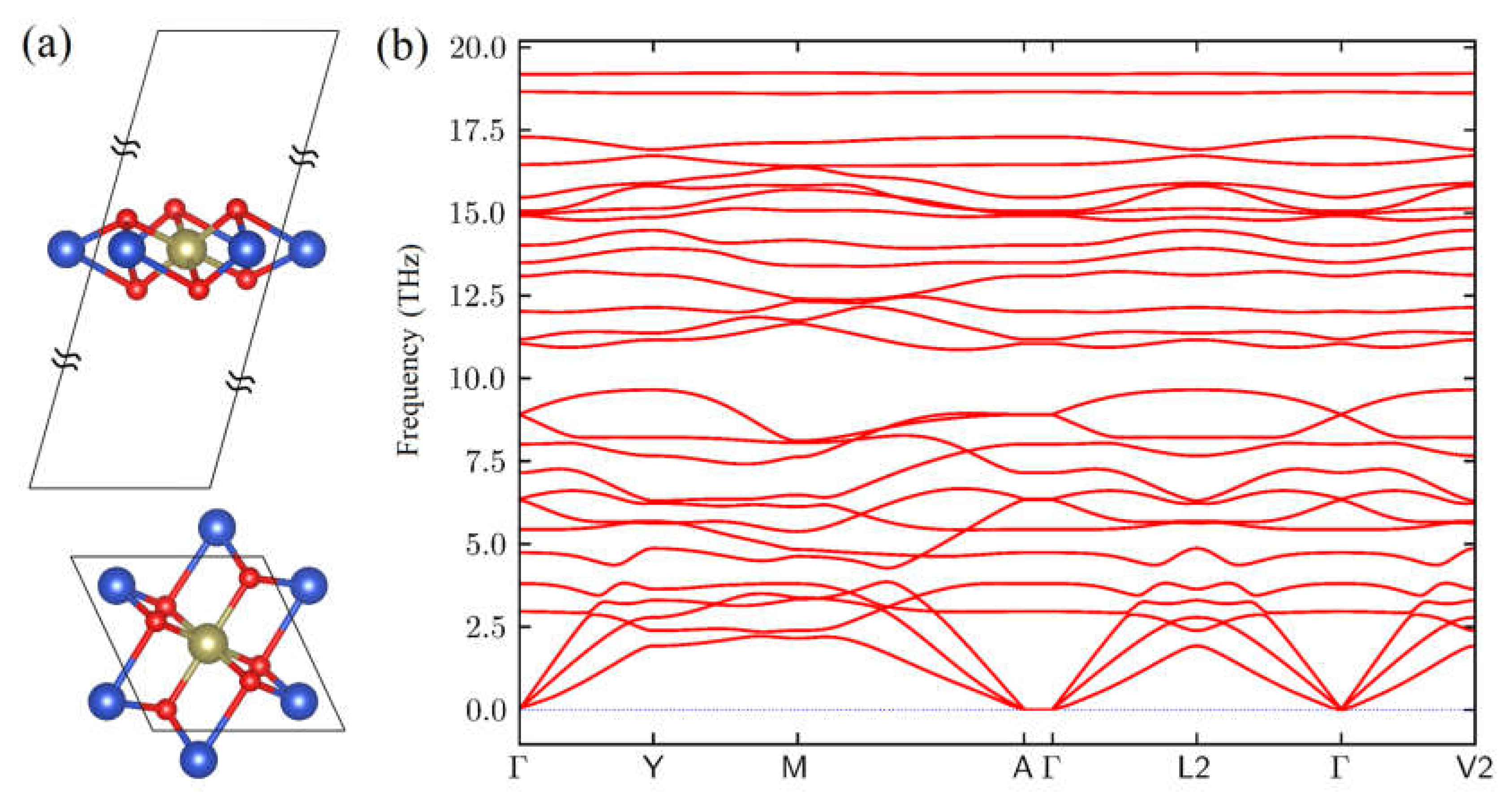
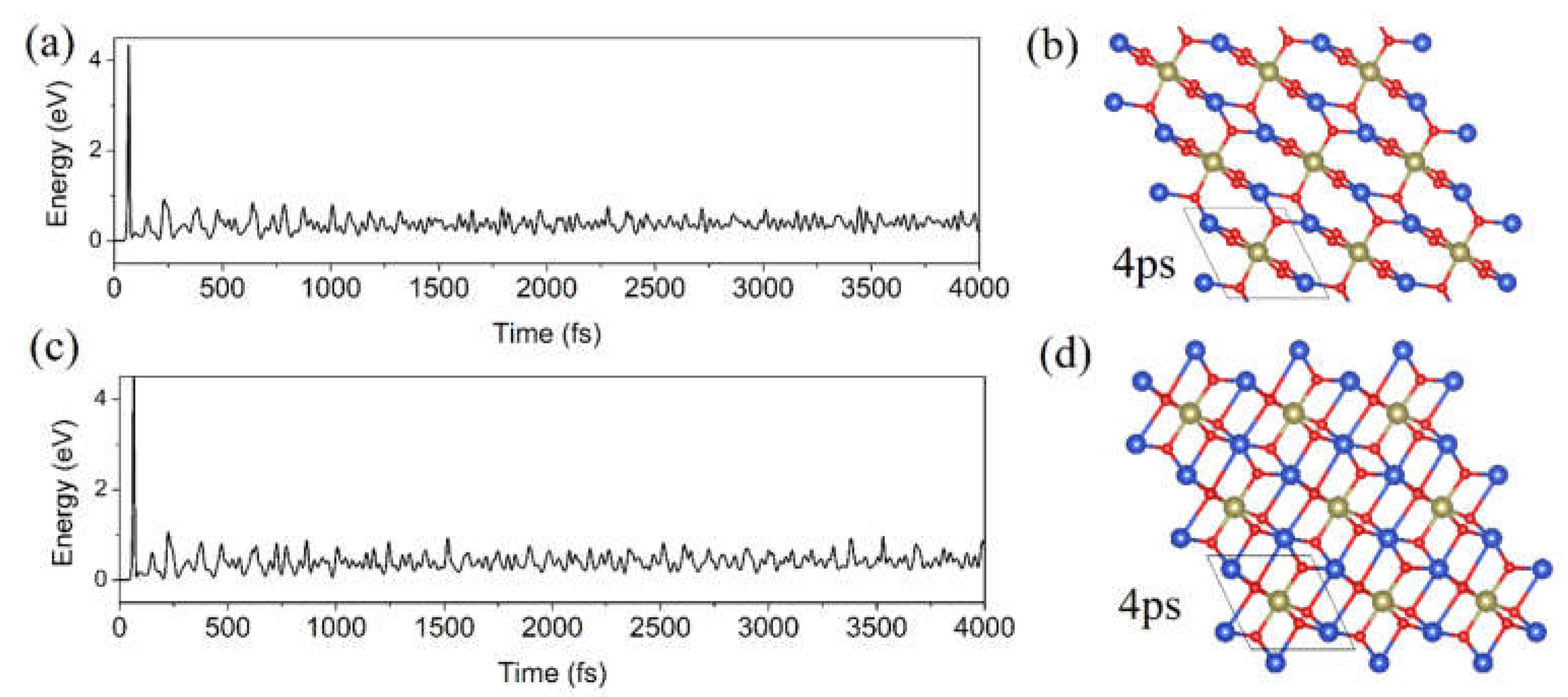
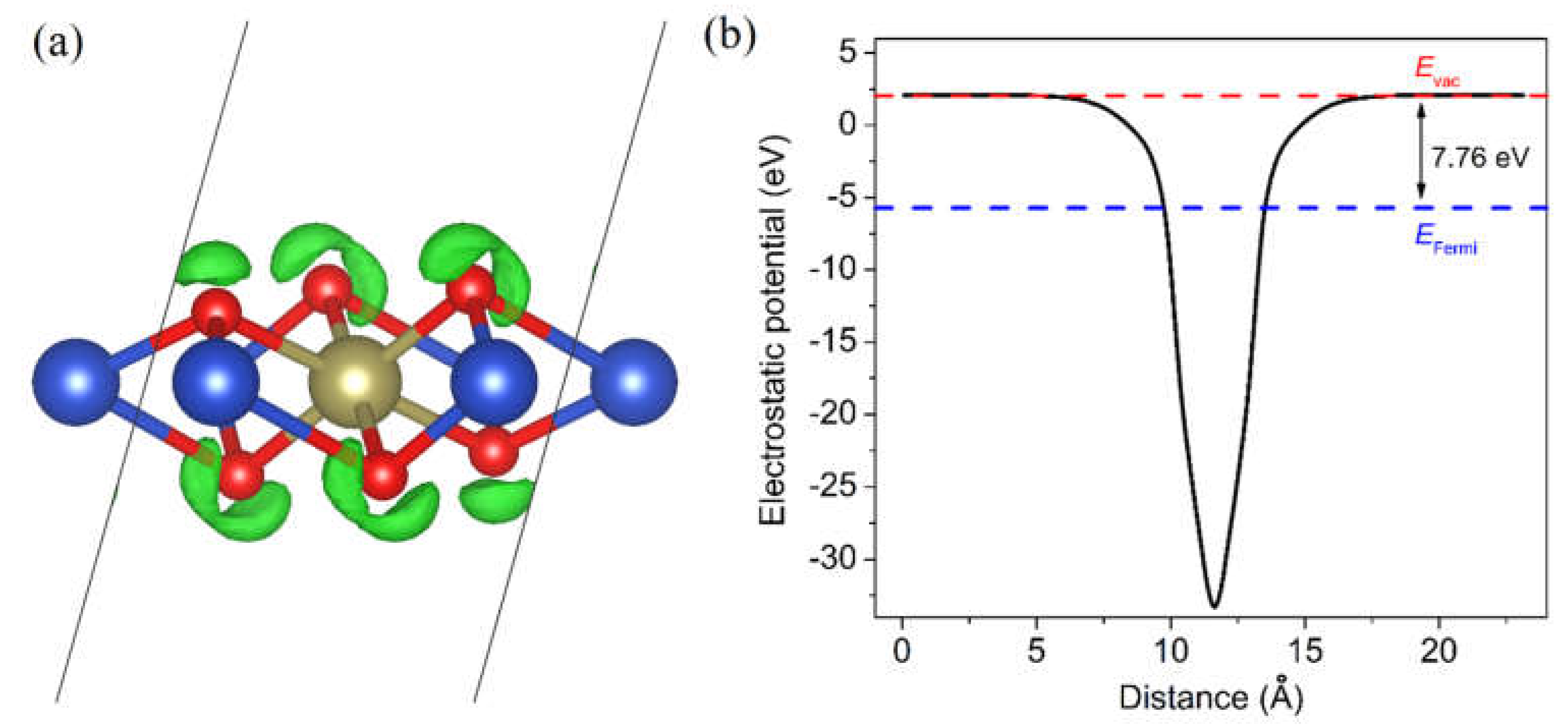
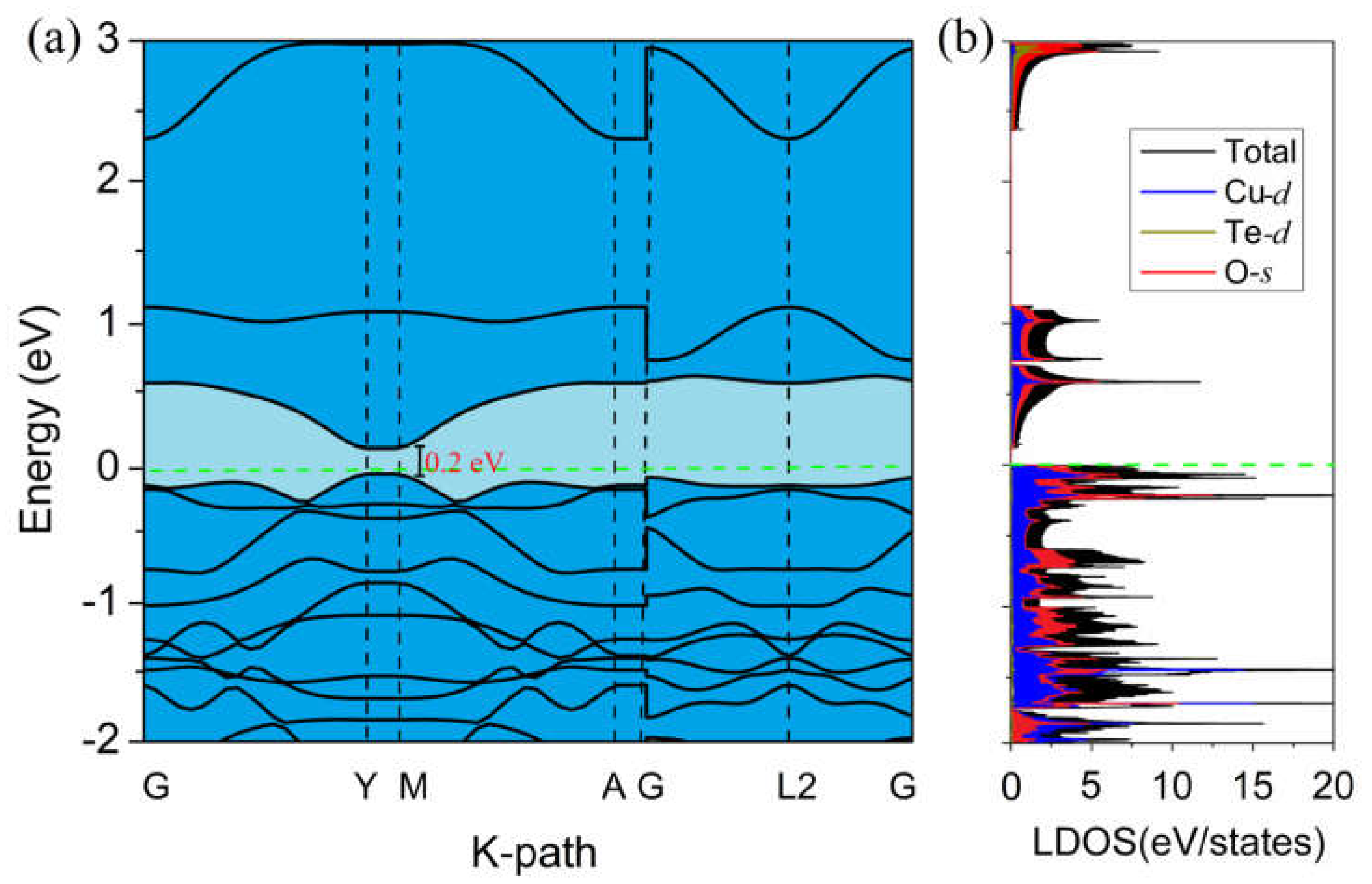
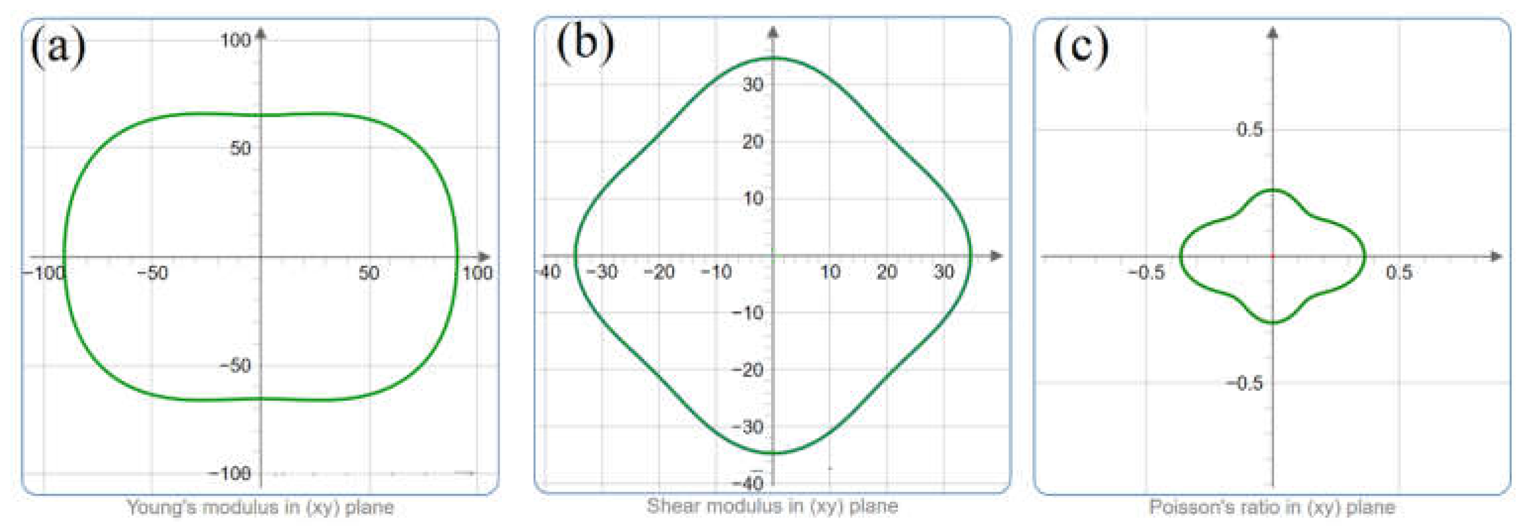
The unit cell structure of the Cu2TeO6 monolayer was designed based on the geometry of primitive unit cell of a bulk Cu2TeO6, which was available in the Materials Project database (mp-1188594) [30]. The structural and thermodynamic stabilities of the optimized unit cell were defined based on the phonon dispersion spectra using the Phonopy code [31] and ab initio molecular dynamics (AIMD) calculations [32]. Calculations were performed using the plane-wave method and implemented in the Vienna Ab initio Simulation Package [33]. The calculations were performed using the Perdew−Burke−Ernzerhof (PBE) exchange−correlation functional under the generalized gradient approximation (GGA) [34]. The optimization was stopped once all of the components of all of the atomic forces were smaller than 10−4 eV/Å and the change in total energy was less than 10−8 eV. The first Brillouin zone was sampled with a 12 × 12 × 1 k-mesh grid, and the kinetic energy cut-off of 520 eV was selected. The periodic boundary conditions were applied for the two in-plane transverse directions, while a vacuum space of 20 Å was introduced to the direction that was perpendicular to the surface plane. The methodology for the calculation of the mechanical properties can be found in previous works [35,36].

3. Results

The atomic structure of the predicted Cu2TeO6 monolayer is shown in Figure 1a. It has a monoclinic unit cell, similarly to its bulk counterpart. Structural parameters of the predicted Cu2TeO6 monolayer can be found in Table 1. Firstly, to show a kinetic stability of the predicted Cu2TeO6 monolayer, the phonon dispersion spectra along the high symmetry directions Γ→Y→M→A→Γ→L2→Γ→V2 of the Brillouin zone for the Cu2TeO6 monolayer were calculated. According to Figure 1b, the phonon dispersion curves of the Cu2TeO6 monolayer are positive in whole of the Brillouin zone, and the transverse, longitudinal, and out-of-plane acoustic modes show a normal linear dispersion around the Γ point, which confirms the kinetic stability of the Cu2TeO6 monolayer.
Thermal stability of the Cu2TeO6 monolayer is verified though the estimation of its formation energy Eform:
Eform = EtotNCu·ECuNTe·ETeNO·EO
where Etot is the total energy of the Cu2TeO6 monolayer, ECu, ETe, and EO are the energies of single Cu, Te, and O atoms, and NCu, NTe, and NO are the numbers of the Cu, Te, and O atoms. The negative Eform = −1.72 eV/atom that was found suggests the thermodynamic stability of the Cu2TeO6 monolayer.
To confirm the thermal stability of the materials, AIMD simulations conducted at a room temperature of 300 K are usually used. Figure 2a shows the total energy fluctuation of the Cu2TeO6 monolayer system at 300 K for the time of 4 ps. It can be seen that there were no artificial energy fluctuations. In addition, according to Figure 2b, there were no visible changes in the structure of the Cu2TeO6 monolayer happening after 4 ps, which suggests its thermal stability. To clarify the application temperature range of Cu2TeO6 monolayer, its stability at higher temperature of 320 K for the time of 4 ps was also evaluated via an AIMD simulation. Figure 2c presents the total energy fluctuation of the Cu2TeO6 monolayer system at 320 K for the time of 4 ps. It is seen that there are also no artificial energy fluctuations. In addition, according to Figure 2d, there were no structural changes in the Cu2TeO6 monolayer after 4 ps, which suggests its thermal stability at 320 K.
To identify the bonding type in the Cu2TeO6 monolayer, the electron localization function (ELF) is simulated and analyzed. It is known that the ELF value, which is in the range from 0 to 1, reflects the degree of charge localization in the real space, where the values close to 0 represent the existence a free electronic state, while the values close to 1 represent a perfect electron localization [37,38,39]. The ELF plot for the Cu2TeO6 monolayer with the isosurface value of 0.70 is presented in Figure 3a. According to Figure 3a, the electron localization is high at the regions around the sites of the O anions, while at the Cu and Te cations sites the value of ELF is low. A large difference found in the ELF plot proposes the existence of an ionic bonding in the Cu2TeO6 monolayer. This conclusion is in line with the fact that an ionic type of bond is characteristic of the bonded metal and non-metal, the difference in the electronegativity of which is higher than 1.5. Particularly, the electronegativity of O (3.5) and Cu (1.9) is higher 1.5, and the electronegativity of Te (2.1) is lower the electronegativity of O (3.5) by 1.4.
The work function (WF) is a critical parameter to characterize a material [40]. It is defined as follows:
WF = EvacEFermi
where Evac is the energy level of a stationary electron in the vacuum, and EFermi corresponds to the Fermi level of the system. The calculated WF of the Cu2TeO6 monolayer is found to be 7.76 eV, as shown in Figure 3b, which is much higher than it is for the most of the 2D materials such as graphene (4.60 eV) [41] and borophene (5.31 eV) [38] and 2D metal chlorides [35] and bulk metals [41] such as Ni (5.23 eV) and Pt (5.65 eV). Importantly, the materials with such a high WF value can be efficiently integrated, for instance, in photovoltaic devices based on a high-WF material/low-WF material hybrid junctions [42].
The calculated band structure and the local density of states (LDOS) of the Cu2TeO6 monolayer are shown in Figure 4. It is predicted that the Cu2TeO6 monolayer is a direct band gap semiconductor with the conduction band minimum (CBM) and valence band maximum (VBM) located at the Y and M points, and its band gap size is found to be 0.20 eV (Figure 4a). According to the LDOS plot in Figure 4b, both the CBM and VBM of the Cu2TeO6 monolayer are formed of the Cu d states and O p states. Such a narrow band gap monolayer semiconductors can be used in infrared nanodetectors [43].
The mechanical stability of the Cu2TeO6 monolayer is also evaluated using the conditions presented by Mazdziarz [44]. As the elastic tensor is calculated based on the periodic boundary conditions, an arbitrary vacuum is presented in the out-of-plane direction when one is dealing with the monolayer. Therefore, the output values of the calculated elastic constants should be correct by eliminating the arbitrariness of the vacuum padding. Particularly, the Cij components (i, j ≠ 3) should be adjusted by multiplying them by the length of the vacuum padding [45]. For the considered Cu2TeO6 monolayer elastic constants matrix is further calculated, the values of the obtained elastic constants Cij are collected in Table 2. According to [44], the mechanical stability criteria for the oblique Bravais lattice are the following:
  C 11 > 0
C 11 C 22   >   C 12 2
det   ( C i j )   >   0
Based on the data presented in Table 2, the Cu2TeO6 monolayer is found to be mechanically stable as it satisfies the criteria in Equation (3). In addition, the mechanical properties of the Cu2TeO6 monolayer such as Young’s modulus, Poisson’s ratio, and the shear modulus are calculated.
Young’s modulus of the monolayer for strains in the x and y directions can be calculated as [46,47]:
E x   = C 11 C 22 C 12 2 C 11 ,   and   E y = C 11 C 22 C 12 2 C 22
The shear modulus of the monolayer can be calculated as [46,47]:
G = C66
Poisson’s ratio of the monolayer in the x and y directions can be calculated as [46,47]:
v x   = C 12 C 11 ,   and   v y     = C 12 C 22
The spatial dependence of Young’s modulus, the shear modulus, and Poisson’s ratio of the Cu2TeO6 monolayer are presented in Figure 5. It is found that these quantities are direction dependent. Young’s moduli of the Cu2TeO6 monolayer in the x and y directions are found to be Ex = 65.95 N/m and Ey = 91.04 N/m, respectively. The shear modulus of the Cu2TeO6 monolayer is found to be G = 34.65 N/m. Poisson’s ratios of the Cu2TeO6 monolayer in the x and y directions are found to be vx = 0.21 and vy = 0.37, respectively.

4. Discussion and Conclusions

In this work, a novel material, the Cu2TeO6 monolayer, is discovered. Its dynamic and thermal stability is studied and confirmed. Importantly, an application of the Cu2TeO6 monolayer is possible at various temperature conditions and geographical locations, from Nordic countries to the tropics, as its stability is confirmed at a room temperature of 300 K and at the elevated temperature of 320 K.
It is found that the Cu2TeO6 monolayer exhibits a narrow band gap of 0.2 eV and a high WF value of 7.76 eV. In addition, the Cu2TeO6 monolayer has anisotropic mechanical properties with the highest Young’s modulus of 91.04 N/m, shear modulus of 34.65 N/m, and Poisson’s ratio of 0.37.
These properties make the Cu2TeO6 monolayer a good candidate for applications in various nanodevices. Particularly, due to its exceptionally high WF value, the Cu2TeO6 monolayer is a good candidate material for photovoltaic devices [42], metal–insulator–metal capacitors [48], and high-WF anodes [49], etc. In addition, despite the Young’s modulus of the Cu2TeO6 monolayer being ~3 time lower than that of graphene [50], which suggests its lower stiffness compared to graphene, the Cu2TeO6 monolayer possesses higher elasticity relative to graphene [51]. This offers the application of the Cu2TeO6 monolayer in straintronic nanodevices [52].

Author Contributions

Conceptualization, methodology, software, validation, formal analysis, investigation, data curation, visualization, A.A.K.; writing—original draft preparation, E.A.K., V.A.B. and A.A.K.; supervision, resources, project administration, funding acquisition, E.A.K. All authors have read and agreed to the published version of the manuscript.

Funding

A.A.K. and V.A.B. are grateful for financial support to the Ministry of Science and Higher Education of the Russian Federation within the framework of the state task of the USATU (No. 075-03-2022-318/1) of the youth research laboratory «Metals and Alloys under Extreme Impacts». E.A.K. acknowledges the support of Grant NSh-4320.2022.1.2 of the President of the Russian Federation for state support of young Russian scientists/candidates of sciences and doctors of sciences.

Institutional Review Board Statement

Not applicable.

Informed Consent Statement

Not applicable.

Data Availability Statement

The datasets are available from the authors on a reasonable request ([email protected]).

Acknowledgments

The authors express their gratitude to the Joint Supercomputer Center of the Russian Academy of Sciences for providing access to cluster computational resources. A.A.K. grateful Javier Fernández-Catalá for the discussions on the possible structure of the Cu2TeO6 monolayer.

Conflicts of Interest

The authors declare no conflict of interest.

References

  1. Xiao, L.; Zhengchen, W.; Wenbin, Y.; Liting, Y.; Renchao, C. Self-assembly MXene-rGO/CoNi film with massive continuous heterointerfaces and enhanced magnetic coupling for superior microwave absorber. Nano-Micro Lett. 2022, 14, 73. [Google Scholar]
  2. Xu, J.; Assoud, A.; Soheilnia, N.; Derakhshan, S.; Cuthbert, H.; Greedan, J.; Whangbo, M.; Kleinke, H. Synthesis, structure, and magnetic properties of the layered copper(II) oxide Na2Cu2TeO6. Inorg. Chem. 2005, 44, 5042–5046. [Google Scholar] [CrossRef] [PubMed]
  3. Golberg, D.; Bando, Y.; Tang, C.; Zhi, C. Boron nitride nanotubes. Adv. Mater. 2007, 19, 2413–2432. [Google Scholar] [CrossRef]
  4. Liu, Z.; Song, L.; Zhao, S.; Huang, J.; Ma, L.; Zhang, J.; Lou, J.; Ajayan, P.M. Direct growth of graphene/hexagonal boron nitride stacked layers. Nano Lett. 2011, 11, 2032–2037. [Google Scholar] [CrossRef] [PubMed]
  5. Mahatha, S.; Patel, K.; Menon, K. Electronic structure investigation of MoS2 and MoSe2 using angle-resolved photoemission spectroscopy and ab initio band structure studies. J. Phys. Condens. Matter. 2012, 24, 475504. [Google Scholar] [CrossRef]
  6. Pumera, M.; Loo, A. Layered transition-metal dichalcogenides (MoS2 and WS2) for sensing and biosensing. TrAC—Trends Anal. Chem. 2014, 61, 49–53. [Google Scholar] [CrossRef]
  7. Gogotsi, Y.; Anasori, B. The Rise of MXenes. ACS Nano 2019, 13, 8491–8494. [Google Scholar] [CrossRef] [Green Version]
  8. Chabi, S.; Kadel, K. Two-dimensional silicon carbide: Emerging direct band gap semiconductor. Nanomaterials 2020, 10, 2226. [Google Scholar] [CrossRef]
  9. Lei, S.; Ge, L.; Liu, Z.; Najmaei, S.; Shi, G.; You, G.; Lou, J.; Vajtai, R.; Ajayan, P. Synthesis and photoresponse of large GaSe atomic layers. Nano Lett. 2013, 13, 2777–2781. [Google Scholar] [CrossRef] [Green Version]
  10. Joshua, E.G. Progress, challenges, and opportunities in two-dimensional materials beyond graphene. ACS Nano 2014, 7, 2898–2962. [Google Scholar]
  11. Xu, Y.; Sprick, R.; Brownbill, N.; Blanc, F.; Li, Q.; Ward, J.; Ren, S.; Cooper, A. Bottom-up wet-chemical synthesis of a two-dimensional porous carbon material with high supercapacitance using a cascade coupling/cyclization route. J. Mater. Chem. A 2021, 9, 3303–3308. [Google Scholar] [CrossRef]
  12. Hamzan, N.B.; Goh, B.T.; Yeoh, K.H.; Chew, K.H. Size-controllable synthesis of 2D Mn3O4 triangular-shaped nanosheets by thermal chemical vapor deposition. Phys. E Low-Dimens. Syst. Nanostruct. 2022, 142, 115273. [Google Scholar] [CrossRef]
  13. Coleman, J.N. Liquid exfoliation of layered materials. Science 2013, 334, 72–75. [Google Scholar]
  14. Xie, Y. Ultrathin black phosphorus nanosheets for efficient singlet oxygen generation. J. Am. Chem. Soc. 2015, 137, 11376–11382. [Google Scholar]
  15. Ma, R.; Sasaki, T. Two-dimensional oxide and hydroxide nanosheets: Controllable high-quality exfoliation, molecular assembly, and exploration of functionality. Acc. Chem. Res. 2015, 48, 136–143. [Google Scholar] [CrossRef]
  16. Al-Ghiffari, A.D.; Ludin, N.A.; Davies, M.L.; Yunus, R.M.; Suait, M.S. Systematic review of molybdenum disulfide for solar cell applications: Properties, mechanism and application. Mater. Today Commun. 2022, 32, 104078. [Google Scholar] [CrossRef]
  17. Ji, W.; Zhao, G.; Hu, G.; Fan, L.; Deng, H.; Fu, Q. The enhancement in dielectric properties for PVDF based composites due to the incorporation of 2D TiO2 nanobelt containing small amount of MWCNTs. Compos. Part A Appl. Sci. 2021, 149, 106493. [Google Scholar] [CrossRef]
  18. Zhang, Y.; Xu, W.; Liu, G.; Zhang, Z.; Zhu, J.; Li, M. Bandgap prediction of two-dimensional materials using machine learning. PLoS ONE 2021, 16, e0255637. [Google Scholar] [CrossRef]
  19. Hanaor, D.A.H.; Assadi, M.H.N.; Li, S.; Yu, A.; Sorrell, C.C. Ab initio study of phase stability in doped TiO2. Comput. Mech. 2012, 50, 185–194. [Google Scholar] [CrossRef] [Green Version]
  20. Kabiraj, A.; Jain, T.; Mahapatra, S. Massive Monte Carlo simulations-guided interpretable learning of two-dimensional Curie temperature. Patterns 2022, 3, 100625. [Google Scholar] [CrossRef]
  21. Li, Y.; Yu, C.; Gan, Y.; Jiang, P.; Yu, J.; Ou, Y.; Zou, D.F.; Huang, C.; Wang, J.; Jia, T.; et al. Mapping the elastic properties of two-dimensional MoS2 via bimodal atomic force microscopy and finite element simulation. NPJ Comput. Mater. 2018, 4, 49. [Google Scholar] [CrossRef]
  22. Pramchu, S.; Srisakonsub, P.; Sucharitakul, S.; Jaroenjittichai, A.P.; Laosiritaworn, Y. First-principles prediction of strain-induced Dirac semimetal state and negative Poisson’s ratio in TiZrB4 monolayer. Comput. Condens. Matter. 2022, 31, e00679. [Google Scholar] [CrossRef]
  23. Mellaerts, S.; Meng, R.; Menghini, M.; Afanasiev, V.; Seo, J.W.; Houssa, M.; Locquet, J.P. Two dimensional V2O3 and its experimental feasibility as robust room-temperature magnetic Chern insulator. NPJ 2D Mater. Appl. 2021, 5, 65. [Google Scholar] [CrossRef]
  24. Xiao, H.; Liang, S.; Xu, L.; Wang, R.; Yang, C. 2D high temperature ferromagnetic Co2Ti2Sn2 monolayer with tunable magnetic anisotropy and superior mechanical flexibility: A first-principles and Monte Carlo study. Phys. E Low-Dimens. Syst. Nanostruct. 2022, 135, 114939. [Google Scholar] [CrossRef]
  25. Sun, W.; Li, Y.; Wang, B.; Jiang, X.; Katsnelson, M.; Korzhavyi, P.; Eriksson, O.; Marco, I. A new 2D monolayer BiXene, M2C (M = Mo, Tc, Os). Nanoscale 2016, 8, 15753–15762. [Google Scholar] [CrossRef] [Green Version]
  26. Bandyopadhyay, A.; Frey, N.C.; Jariwala, D.; Shenoy, V.B. Engineering magnetic phases in two-dimensional non-van der Waals transition-metal oxides. Nano Lett. 2019, 19, 7793–7800. [Google Scholar] [CrossRef]
  27. Puthirath Balan, A.; Radhakrishnan, S.; Woellner, C.F.; Sinha, S.K.; Deng, L.; Reyes, C.D.L. Exfoliation of a non-van der Waals material from iron ore hematite. Nat. Nanotechnol. 2018, 13, 602–609. [Google Scholar]
  28. Balan, A.P.; Radhakrishnan, S.; Kumar, R.; Neupane, R.; Sinha, S.K.; Deng, L. A Non-van der Waals two-dimensional material from natural titanium mineral ore ilmenite. Chem. Mater. 2018, 30, 5923–5931. [Google Scholar] [CrossRef]
  29. The Materials Project. Materials Data on Cu2TeO6 by Materials Project; Lawrence Berkeley National Laboratory: Berkeley, CA, USA, 2019. [Google Scholar] [CrossRef]
  30. Jain, A.; Ong, S.P.; Hautier, G.; Chen, W.; Richards, W.D.; Dacek, S.; Cholia, S.; Gunter, D.; Skinner, D.; Ceder, G.; et al. Commentary: The Materials Project: A materials genome approach to accelerating materials innovation. APL Mater. 2013, 1, 11002. [Google Scholar] [CrossRef] [Green Version]
  31. Togo, A.; Tanaka, I. First-principles phonon calculations in materials science. Scr. Mater. 2015, 108, 1–5. [Google Scholar] [CrossRef] [Green Version]
  32. Henkelman, G.; Uberuaga, B.P.; Jonsson, H. A Climbing image nudged elastic band method for finding saddle points and minimum energy paths. J. Chem. Phys. 2000, 113, 9901. [Google Scholar] [CrossRef] [Green Version]
  33. Kresse, G.; Furthmuller, J. Efficient iterative schemes for ab initio total-energy calculations using a plane-wave basis set. Phys. Rev. B 1996, 54, 11169. [Google Scholar] [CrossRef]
  34. Perdew, J.P.; Burke, K.; Ernzerhof, M. Generalized gradient approximation made simple. Phys. Rev. Lett. 1996, 77, 3865–3868. [Google Scholar] [CrossRef] [PubMed] [Green Version]
  35. Kistanov, A.A.; Shcherbinin, S.A.; Botella, R.; Davletshin, A.; Cao, W. Family of two-dimensional transition metal dichlorides: Fundamental properties, structural defects, and environmental stability. J. Phys. Chem. Lett. 2022, 13, 2165–2172. [Google Scholar] [CrossRef]
  36. Shcherbinin, S.A.; Zhou, K.; Dmitriev, S.V.; Korznikova, E.A.; Davletshin, A.R.; Kistanov, A.A. Two-dimensional black phosphorus carbide: Rippling and formation of nanotubes. J. Phys. Chem. C 2018, 124, 10235–10243. [Google Scholar] [CrossRef] [Green Version]
  37. Sun, P.-P.; Kripalani, D.R.; Bai, L.; Chi, W.; Zhou, K. A highly efficient electron transport layer for perovskite solar cells. J. Phys. Chem. C 2021, 125, 5372–5379. [Google Scholar] [CrossRef]
  38. Kistanov, A.A.; Cai, Y.; Zhou, K.; Srikanth, N.; Dmitriev, S.V.; Zhang, Y.-W. Exploring the charge localization and band gap opening of borophene: A first-principles study. Nanoscale 2018, 10, 1403–1410. [Google Scholar] [CrossRef] [Green Version]
  39. Grin, Y.; Savin, A.; Silvi, B. The Chemical Bond: Fundamental Aspects of Chemical Bonding; Frenking, G., Shaik, S., Eds.; Wiley-VCH: Weinheim, Germany, 2014; Volume 1, p. 345. [Google Scholar]
  40. Cai, Y.; Zhang, G.; Zhang, Y.-W. Layer-dependent band alignment and work function of few-layer phosphorene. Sci. Rep. 2014, 4, 6677. [Google Scholar] [CrossRef] [Green Version]
  41. Lee, E.J.H.; Balasubramanian, K.; Weitz, R.T.; Burghard, M.; Kern, K. Contact and edge effects in graphene devices. Nat. Nanotechnol. 2008, 3, 486–490. [Google Scholar] [CrossRef]
  42. Chen, C.; Jin, T.; Wei, L.; Yong, L.; Xiaodong, L.; Wang, Y.; Zhang, L.; Liao, C.; Hu, N.; Song, C.; et al. High-work-function metal/carbon nanotube/low-work-function metal hybrid junction photovoltaic device. NPG Asia Mater. 2015, 7, e220. [Google Scholar] [CrossRef] [Green Version]
  43. Zhao, M.; Xia, W.; Wang, Y.; Luo, M.; Tian, Z.; Guo, Y.; Hu, W.; Xue, J. Nb2SiTe4: A stable narrow-gap two-dimensional material with ambipolar transport and mid-infrared response. ACS Nano 2019, 13, 10705–10710. [Google Scholar] [CrossRef] [PubMed] [Green Version]
  44. Maździarz, M. Comment on ‘The Computational 2D Materials Database: High-throughput modeling and discovery of atomically thin crystals’. 2D Mater. 2019, 6, 48001. [Google Scholar] [CrossRef] [Green Version]
  45. Singh, S.; Langa, L.; Dovale-Farelo, V.; Herath, U.; Tavadze, P.; Coudert, F.-X.; Romero, A.H.A. MechElastic: Python library for analysis of mechanical and elastic properties of bulk and 2D materials. Comput. Phys. Commun. 2021, 267, 108068. [Google Scholar] [CrossRef]
  46. Andrew, R.C.; Mapasha, R.E.; Ukpong, A.M.; Chetty, N. Mechanical properties of graphene and boronitrene. Phys. Rev. B 2012, 85, 125428. [Google Scholar] [CrossRef]
  47. Zhao, T.; Zhang, S.; Guo, Y.; Wang, Q. TiC2: A new two-dimensional sheet beyond MXenes. Nanoscale 2016, 8, 233–242. [Google Scholar] [CrossRef]
  48. Kim, Y.W.; Lee, A.J.; Han, D.H.; Lee, D.C.; Hwang, H.; Kim, Y.; Moon, S.; Youn, T.; Lee, M.; Jeon, W. Reliable high work-function molybdenum dioxide synthesis via template-effect-utilizing atomic layer deposition for next-generation electrode applications. J. Mater. Chem. C 2022, 10, 12957–12965. [Google Scholar] [CrossRef]
  49. Chun, J.-Y.; Han, J.-W.; Seo, D.-S. Application of high work function anode for organic light emitting diode. Mol. Cryst. Liq. Cryst. 2009, 514, 115–121. [Google Scholar] [CrossRef]
  50. Lajevardipour, A.; Neek-Amal, M.; Peeters, F.M. Thermomechanical properties of graphene: Valence force field model approach. J. Phys. Condens. Matter. 2012, 24, 175303. [Google Scholar] [CrossRef] [Green Version]
  51. Cadelano, E.; Palla, P.L.; Giordano, S.; Colombo, L. Elastic properties of hydrogenated graphene. Phys. Rev. B 2010, 82, 235414. [Google Scholar] [CrossRef] [Green Version]
  52. Miao, F.; Liang, S.-J.; Cheng, B. Straintronics with van der Waals materials. NPJ Quantum Mater. 2021, 6, 59. [Google Scholar] [CrossRef]
Figure 1. The atomic structure of the unit cell (a) and phonon dispersion curve (b) for the Cu2TeO6 monolayer.
Applsci 13 00815 g001
Figure 2. Total energy fluctuation obtained from AIMD simulations conducted at 300 K (a) and 320 K (c) for the time of 4 ps for the Cu2TeO6 monolayer. The atomic structure of the Cu2TeO6 monolayer at 300 K (b) and 320 K (d) after 4 ps.
Applsci 13 00815 g002
Figure 3. ELF with the isosurface value of 0.70 for the Cu2TeO6 monolayer (a) and WF for the Cu2TeO6 monolayer (b).
Applsci 13 00815 g003
Figure 4. Band structure (a) and LDOS (b) for the Cu2TeO6 monolayer. The Fermi level is represented by the dashed green line.
Applsci 13 00815 g004
Figure 5. Spatial dependencies of (a) the Young’s modulus, (b) the shear modulus, and (c) Poisson’s ratio for the Cu2TeO6 monolayer.
Applsci 13 00815 g005
Table 1. Structural parameters of the Cu2TeO6 monolayer.
a5.272 Å
b5.272 Å
α100.25
β100.25
γ112.43
Table 2. The calculated elastic constants Cij for the Cu2TeO6 monolayer.
C11101.18 N/m
C2273.29 N/m
C1227.26 N/m
C4434.65 N/m
Disclaimer/Publisher’s Note: The statements, opinions and data contained in all publications are solely those of the individual author(s) and contributor(s) and not of MDPI and/or the editor(s). MDPI and/or the editor(s) disclaim responsibility for any injury to people or property resulting from any ideas, methods, instructions or products referred to in the content.

