Article

Study of Structure, Morphology and Optical Properties of Cobalt-Doped and Co/Al-co-Doped ZnO Thin Films Deposited by Electrospray Method

Institute of Optical Materials and Technologies “Acad. J. Malinowski”, Bulgarian Academy of Sciences, Akad. G. Bonchev Str., bl. 109, 1113 Sofia, Bulgaria
*
Author to whom correspondence should be addressed.
Appl. Sci. 2023, 13(17), 9611; https://doi.org/10.3390/app13179611
Submission received: 30 July 2023 / Revised: 17 August 2023 / Accepted: 23 August 2023 / Published: 25 August 2023
(This article belongs to the Special Issue Advances in Surface Science and Thin Films)

Abstract

:
A versatile electrospray method was utilized for deposition of thin ZnO films doped with Co (5%) (CZO) or co-doped with Co (2.5%) and Al (2.5%) (CAZO). Thin polycrystalline films with approximate thickness of 200 nm and high transmittance (more than 80%) were obtained. No additional XRD peaks due to dopant impurities or dopant oxides were observed. The cobalt doping led to decrease in grain size and increase in crystallite size from 22 nm to 29 nm in the (101) direction. Smaller changes were observed for the CAZO films. Surface roughness of the films was measured using a 3D optical profiler. Surface roughness of the doped films was from 5 nm to 9 nm higher than that of the pure films. Refractive index, extinction coefficient and thickness of the films were calculated using ellipsometric measurements and were further used for determination of optical band gap and Urbach energy. Refractive index and optical band gap increased with doping from 1.86 and 3.29 eV for pure ZnO to 2.00 and 3.35 eV for CZO and 1.97 and 3.33 eV for CAZO films. Through calculation of Urbach energy (119 meV for pure ZnO, 236 meV for CZO and 138 meV for CAZO), it was demonstrated that doping leads to an increase in structural disorder, most pronounced in the case of Co doping.

1. Introduction

Zinc oxide (ZnO) belongs to the II–VI semiconductor group and exhibits high exciton binding energy (~60 meV) and high transmittance in the visible and NIR (near-infrared) spectral ranges due to its wide optical bandgap of about 3.3–3.4 eV [1,2]. ZnO is nontoxic and biocompatible with UV emission and piezoelectricity, and has relatively low conductivity due to its low electron concentration [1,2]. ZnO is regarded as a suitable platform for doping with different dopants to achieve the appropriate properties for diverse applications such as transparent conductive electrodes [3], thin film photocatalysts [4,5,6], active media for sensing [7,8,9], antibacterial agents [4,10], and photoanodes for efficient perovskite solar cells [11]. Although the research on ZnO goes back several decades, there has been renewed interest in recent years. One of the sources of this scientific interest is the theoretical prediction of room-temperature ferromagnetism in transition-metal-doped ZnO [12] and its experimental confirmation in Co-doped ZnO [13,14,15]. Thus, along with the applications in optoelectronic devices, ZnO has also been studied as a dilute magnetic semiconductor (DMS) through doping with transition metals (Co, Ni, Mn, etc.) [16,17,18]. DMSs are a class of materials in which a small portion of the host lattice cations is replaced with magnetic impurities. If optically transparent DMSs can be made, they would be very attractive for optospintronic applications [19]. In addition to ferromagnetism, cobalt as a dopant in ZnO is also beneficial for enhancing the photocatalytic performance of ZnO because it suppresses charge carrier recombination, which improves photocatalytic performance [4,20]. A large number of studies have been reported on cobalt-doped ZnO, and various techniques have been implemented for deposition of Co-doped ZnO thin films, including atomic layer deposition [18], pulsed laser deposition [21,22], magnetron sputtering [16,23], chemical bath deposition [24,25], sol-gel combined with spin coating or dip-coating [4,26,27,28] and spray pyrolysis [5,29]. However, simple, versatile, and low-cost deposition techniques that can be performed in an ambient environment are still needed. These techniques could attract wide interest and application if they can produce high-quality thin films with comparable properties to those produced by other means.
We have selected the electrospray (ES) method for film deposition because we have already demonstrated that it offers a simple, scalable, and inexpensive method of deposition of ZnO films and Al-doped ZnO thin films with reproducible properties [30,31]. Structure, morphology, and optical properties can be easily tuned through the variation of deposition parameters [30]. Moreover, there is no need for complicated equipment because ES is performed in air and uses nontoxic and inexpensive precursors and solvents [30]. Unlike the sol-gel method, in the electrospray method postdeposition annealing is not required because both the moderate substrate temperatures (200–300 °C) and small size of the droplets ensure precursor decomposition during film deposition [30].
It is also worth exploring the possibility of implementing the ES method for co-doping using a mixture of appropriate amounts and types of precursors. We have selected Al for co-doping of cobalt-doped ZnO films because it has been shown that co-doping of ZnO with Co and Al enables the synthesis of transparent and conductive materials with specific magnetic properties [32,33]. Furthermore, Khan et al. [34] have recently theoretically studied the effect of Co/Al co-doping of ZnO and have shown that additional electrons introduced by Al change the magnetic ground state of Co-doped ZnO from an antiferromagnetic to a ferromagnetic state, and the estimated Curie temperature is expected to be higher than room temperature.
In this paper, we present the characterization of properties (structure, morphology, surface roughness, refractive index, absorption coefficient, optical band gap and Urbach energy) of cobalt-doped and Co/Al-co-doped ZnO thin films deposited by electrospraying (ES). The successful implementation of ES as a versatile method of deposition of doped and pure ZnO films at moderate temperatures without postdeposition annealing is demonstrated. Cobalt doping and co-doping of ZnO with Al and Co is achieved simply by mixing appropriate amounts of nontoxic and inexpensive precursors (zinc acetate dehydrate, cobalt acetate and aluminum nitrate) and solvents (de-ionized water and ethanol). The impact of doping and co-doping on the films’ properties is revealed and discussed.

2. Materials and Methods

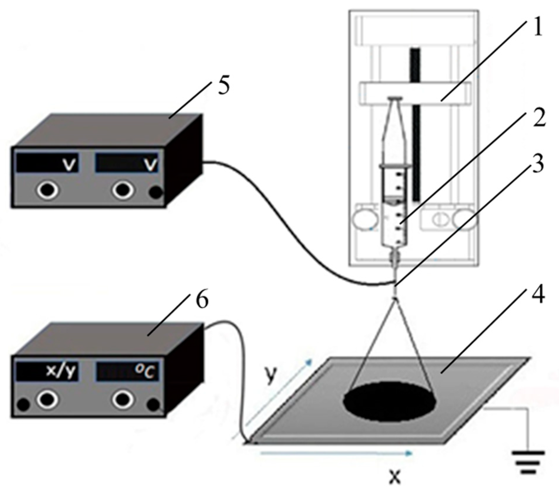
2.1. Thin Film Deposition

Thin films were deposited by the electrospray method using the vertical configuration schematically presented in Figure 1. The setup was equipped with a 5 mL syringe (2) connected to a syringe pump (1) that provides a constant feed rate of the ZnO precursor of 15 μL/min. A voltage of 18 kV was applied via a DC power supply (5) (Applied Kilovolts Ltd., An Adaptas Company, West Sussex, UK) to the emitter (3), which is a stainless-steel needle with inner and outer diameters of 241 and 508 microns, respectively. The film substrate was placed onto a collector (4), which is a stainless-steel-duralumin plate grounded safely and heated to 300 °C by a thermocontrolled heater (6). The emitter-to-collector distance was fixed at 6 cm. In order to obtain homogenous films in the lateral direction, movement in the x-y plane was added during film deposition. The linear rate of the movement was controlled by two motors and a controller (6). The substrate temperature was kept at 300 °C, the deposition time was 60 min, and the approximate film thickness was 200 nm. Two types of substrates were used: silicon wafers 2 inches in diameter and double-polished optical glass with a rectangular shape and dimensions of 24 mm × 36 mm.
The zinc oxide precursor solution was prepared with a two-step process. Firstly, 0.400 g of zinc acetate dehydrate was dissolved in 1.8 mL deionized (DI) water by stirring at room temperature for 5 min. In the second step, the aqueous solution was further diluted by adding 12 mL ethanol and a few drops of acetic acid for clearing. The solution was stirred for 2 h at room temperature. Cobalt acetate and aluminum nitrate were used for doping. Batch solutions with a weight concentration of 10 wt.% were prepared by dissolving cobalt acetate in DI water and aluminum nitrate in ethanol. Appropriate amounts of the batch solutions were mixed with the ZnO precursor solution in order to obtain a 5 wt.% doping level of ZnO, yielding 5% Co-doped ZnO (CZO) and 5% Co/Al-co-doped ZnO (CAZO). The ratio of Co/Al in the latter is 1, i.e., the CAZO film was co-doped with 2.5% Co and 2.5% Al. ZnO films doped with 5% Al (AZO) were also deposited. As mentioned above, the substrate temperature during spraying was kept at 300 °C in order to decompose the initial precursor and oxidize it to ZnO.

2.2. Characterization of Morphology and Structure

Surface morphology of the films was studied using a scanning electron microscope (Philips 515, 30 kV accelerating voltage) and a transmission electron microscope (JEOL JEM 2100, JEOL Ltd., Tokyo, Japan). X-ray diffraction (Philips 1710) (measurement step of 0.025 deg, systematic error of the instrument less than 0.015 degree) and selected area electron diffraction by TEM were used for examination of the crystal status and structure of the films. The samples for TEM investigation were prepared by gently scratching the film’s surface and collecting the detached particles using water, followed by placing a drop on a standard copper grid for direct observation by TEM.

2.3. Characterization of Optical Properties

The refractive index, extinction coefficient/absorption coefficient and thickness of the films were determined by measurement with a phase-modulated spectroscopic ellipsometer (UVISEL 2, Horiba Jobin Yvon, Longjumeau, France) in the spectral range from 250 nm to 820 nm at an incident angle of 70°, while the films’ transmittance spectra were measured with a UV-VIS-NIR spectrophotometer Cary 05E (Varian, Sydney, Australia). An optical profiler (Zeta-20, KLA, Milpitas, CA, USA) was used for measurement of surface roughness of the films over a wide area (75 μm to 90 μm).

3. Results and Discussions

3.1. Surface Morphology
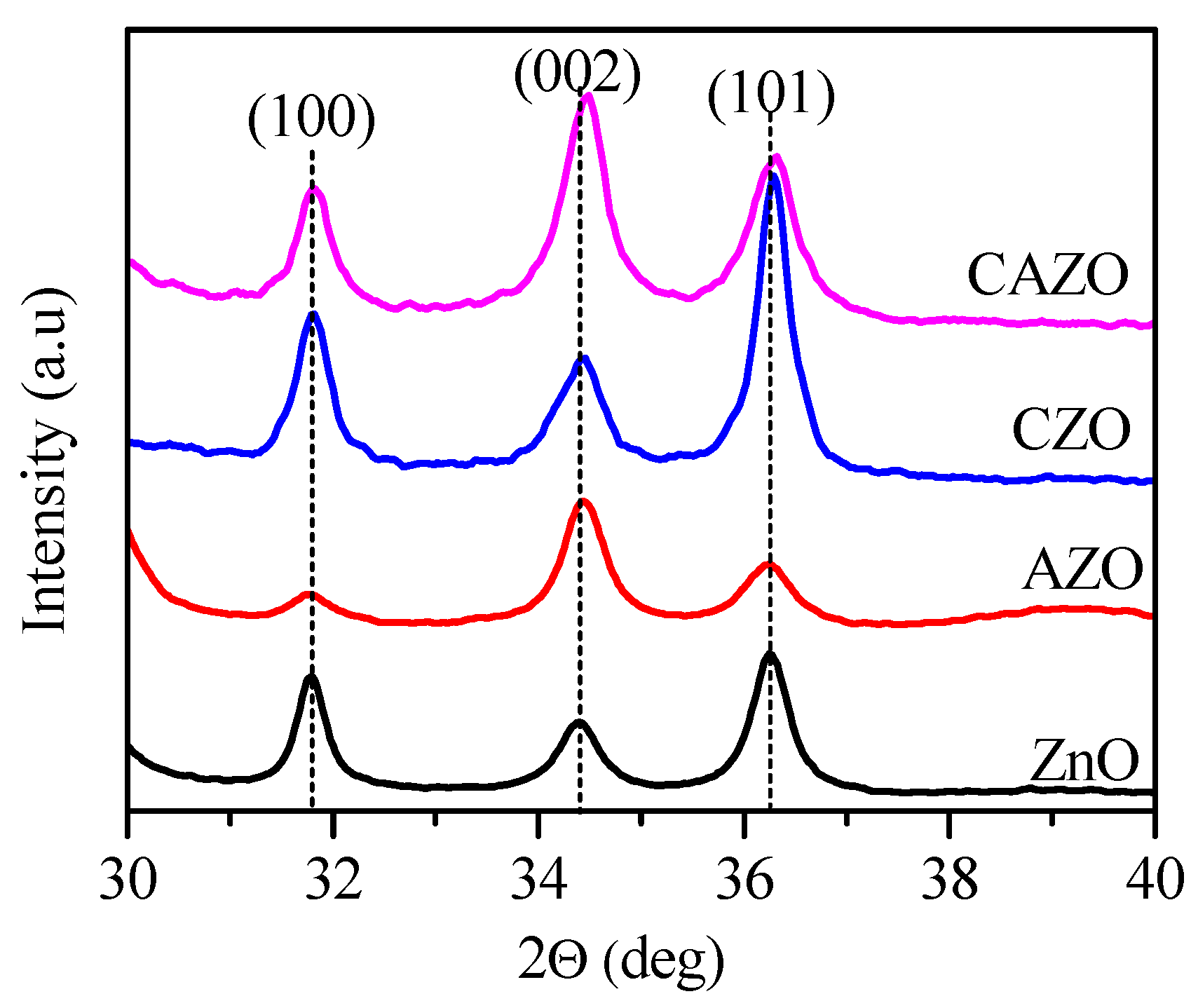
The surface morphology of the films was studied by scanning electron microscopy (SEM). Typical images of the pure ZnO, 5% Co-doped (CZO) and Co/Al-co-doped ZnO (CAZO) are presented in Figure 2. For comparison, films doped with 5% Al (AZO) were also prepared and displayed in Figure 2. SEM images reveal that the surface of all films is granular, with the grain size depending on the type of the dopant. The measured grain size is presented in Table 1. It can be seen that cobalt doping leads to more than twice the decrease in particle size, from 143 nm for pure ZnO to 62 nm for CZO films, while the induced changes in surface morphology are negligible for Al doping (the grain size is 128 nm for AZO films). The surface morphology of CAZO films (Figure 2d) is closer to that of CZO films (Figure 2c), with an average grain size of 71 nm (Figure 2a). In all studied cases, particles are distributed homogenously on the surface without any cracks or pores. The possible reasons for the finer granular morphology for Co-doped films are further discussed in the next section.

3.2. Structure

The structure of the films was studied both by X-ray diffraction (XRD) and selected area electron diffraction (SAED) using TEM. The XRD patterns of ZnO films with different dopants are shown in Figure 3. All films are polycrystalline, with diffraction peaks corresponding to those of polycrystalline wurtzite ZnO. The intensity of the (100) and (101) peaks decreases with Al doping, while Co doping leads to an increase in the intensity of all peaks, particularly in the (101) plane.
To check how doping impacts the crystallinity of the films, the crystallite size was calculated from the positions of the peaks and their full width at half maximum using the Debye–Scherrer formula. From the calculated data presented in Table 1, it can be seen that in general doping does not noticeably change the size of the crystallites, with one exception. In the case of Co doping, the size of the crystallites in the (101) direction increased from 22 nm for ZnO to 29 nm for CZO, an enhancement of more than 30%. The same trend of improved crystallinity was observed by Chanda et al. [17]. The authors assumed that cobalt in ZnO matrix would enhance the nucleation of particles and the growth of crystallites [17]. However, this trend was not observed for CAZO films that also contained Co. Considering that the net concentration of Co in CAZO is half that of CZO, we may conclude that a concentration threshold exists below which an enhancement is not observed. Mir et al. [32] explained the preferential growth in a particular plane in terms of surface energy minimization: the preferred orientation is a result of self-ordering caused by the minimization of the crystal surface force energy. Obviously, more studies are needed to unveil the possible reasons behind the observed preferential growth in the (101) plane for CZO films. However, these are beyond the scope of the present manuscript.
It can be seen from the SEM pictures (Figure 2) and Table 1 that for all studied films, the grain sizes are bigger than the crystallite size calculated from the XRD patterns (Figure 3). This means that the grains on the surface were built from few crystallites (about 6 for pure ZnO and AZO films and about 3 for CZO and CAZO films), so an agglomeration of crystallites took place. The decrease in the grain size in the case of cobalt doping (Figure 2c,d) could be associated with suppression of crystallite agglomeration, possibly due to the higher solubility of Co in the ZnO matrix as compared to Al. Similar suppression of aggregation is clearly evident in [10], but unfortunately no reason is discussed.
On the other hand, the decrease in grain size leads to growth of the attraction forces between crystallites, causing them to aggregate slightly in the case of cobalt doping. Another possible explanation was given by Abdelkrim et al. [5], who attributed the increase in crystallite size to the distortion in the ZnO host lattice by Co impurities, which stimulate the coalescence of the ZnO crystallites [5].
It should be noted that no additional peaks due to dopant impurities or dopant oxides are observed at a 5% doping concentration. This is in line with the results of other authors, who have confirmed the presence of metal Co only at concentrations higher than 10% [22]. Therefore, it may be assumed that both Co and Al ions are incorporated in the ZnO lattice without changing the wurtzite structure. Closer examination of XRD patterns reveals a shift in the peaks’ position toward higher diffraction angles in doped films compared to pure ZnO. The most pronounced changes are for CAZO films, where the (002) and (101) peaks shift by 0.08° and 0.06°, respectively. Decreases in cell volume and lattice spacing due to replacement of Zn ions in the lattice by the smaller Al and Co ions are possible reasons for the observed shift [10,17,27,35].
In order to confirm the assumption of lattice contraction, we conducted TEM studies along with selected area electron diffraction (SAED) (Figure 4). From TEM pictures, it can be seen that all the films have a similar morphology. They consist of nanocrystallites with irregular shapes in the size range of 20–30 nm, which is in accordance with the crystallite size calculated from XRD spectra (Table 1). The SAED patterns of all studied films (for clarity, only the SAED pattern for undoped film is shown in Figure 4) show clearly distinguishable rings corresponding to different planes of hexagonal wurtzite ZnO structures. All SAED patterns were indexed, and d-spacing (also called interplanar distance) was calculated and compared to that for pure ZnO. For all samples, the calculated d-spacing was lower than for undoped films. The deviation varied from 1% to 2% depending on the type of the dopant and crystal orientation. The highest deviations were obtained for AZO (2.03% in the 102 plane), CZO (1.76% in the 102 plane) and CAZO (1.08% in the 002 plane). We should note here that electron diffraction is taken from a very small selected area of the sample, thus giving local information for the sample status. The local SAED results may deviate from global XRD results to some extent. Generally, both techniques clearly confirm that 5% doping leads to lattice contraction. This is a consequence of the replacement of Zn ions in the lattice with the smaller Al and Co ions. Our additional TEM and SAED studies have shown that when concentration of dopants increases to 10%, local areas can be found where lattice spacing increases compared to pure ZnO films. This means that at higher concentration, dopant ions have occupied interstitial sites between zinc and oxygen atoms. Similar results are obtained for AZO films deposited by spray pyrolysis [36]. Two incorporation processes of aluminum in the ZnO lattice were detected: (i) a substitution of Zn2+ by Al3+ for concentrations less than 2%, and (ii) occupation of interstitial sites beyond 2% [36].

3.3. Optical Properties

3.3.1. Transmittance Measurements

Transmittance spectra (T) of films deposited on glass substrates are measured in the spectral range from 320 nm to 900 nm and are plotted in Figure 5 along with the spectra of bare glass substrates. Since the thicknesses of all doped films are similar (around 200 nm), it is appropriate to compare their transmittance spectra and make conclusions about the degree of transparency. It can be seen from Figure 5 that the films are transparent in the VIS-NIR range, although a small decrease in T is observed in doped films, especially cobalt-doped films. Two possible reasons for the observed drop in T in the UV-VIS spectral range are scattering losses and light absorption. To analyze the possibility of small scattering losses, we measured the surface roughness of the films using an optical profiler. The obtained values are presented in Table 2. It can be seen that for the doped films, the surface roughness is from 5 nm to 9 nm higher than the pure film. This could generate some scattering, resulting in the decrease in T. The comparison of the T spectra of doped films shows that AZO film has the highest transmittance, which is very similar to the T-curve of the undoped films. The difference in the spectral position of the peaks is due to a small difference in the film thickness of both films. Therefore, the small increase in the roughness observed for the Al-doped films does not lead to a drop in transmittance of the films. This means that the observed decrease in T for cobalt-doped films is due more to absorption than to scattering. The comparison of the spectral positions of the fundamental absorption edges indicates a slight blue-shifting for the AZO films and noticeable band-tailing for the CZO and CAZO films. Similar band tails were observed by Ivil et al. [22] and Yoo et al. [37] for pulsed-laser-deposited CZO, and were explained by impurities, disorder and point defects [22,37].
Interference patterns due to the multiple reflections from the top and bottom sides of the films is conspicuous in the T spectra of the ZnO and AZO films (Figure 5) and suppressed to some extent in the spectra for the CZO and CAZO films. In the cobalt-doped samples, there are three absorption peaks in the spectral range 550–700 nm, indicated with arrows in Figure 5. These absorption peaks are centered at 560 nm (2.21 eV), 609 nm (2.04 eV) and 655 nm (1.89 eV), and perfectly match the peaks obtained by other groups—2.20 eV, 2.04 eV and 1.88 eV [21].
The absorption peaks are characteristic peaks of Co2+ ions assigned to charge transfers between donor and acceptor ionization levels located within the band gap of the ZnO host [16] and prove the existence of Co at the tetrahedral sites of the ZnO hexagonal wurtzite structure in the form of Co2+ [16,21,28].

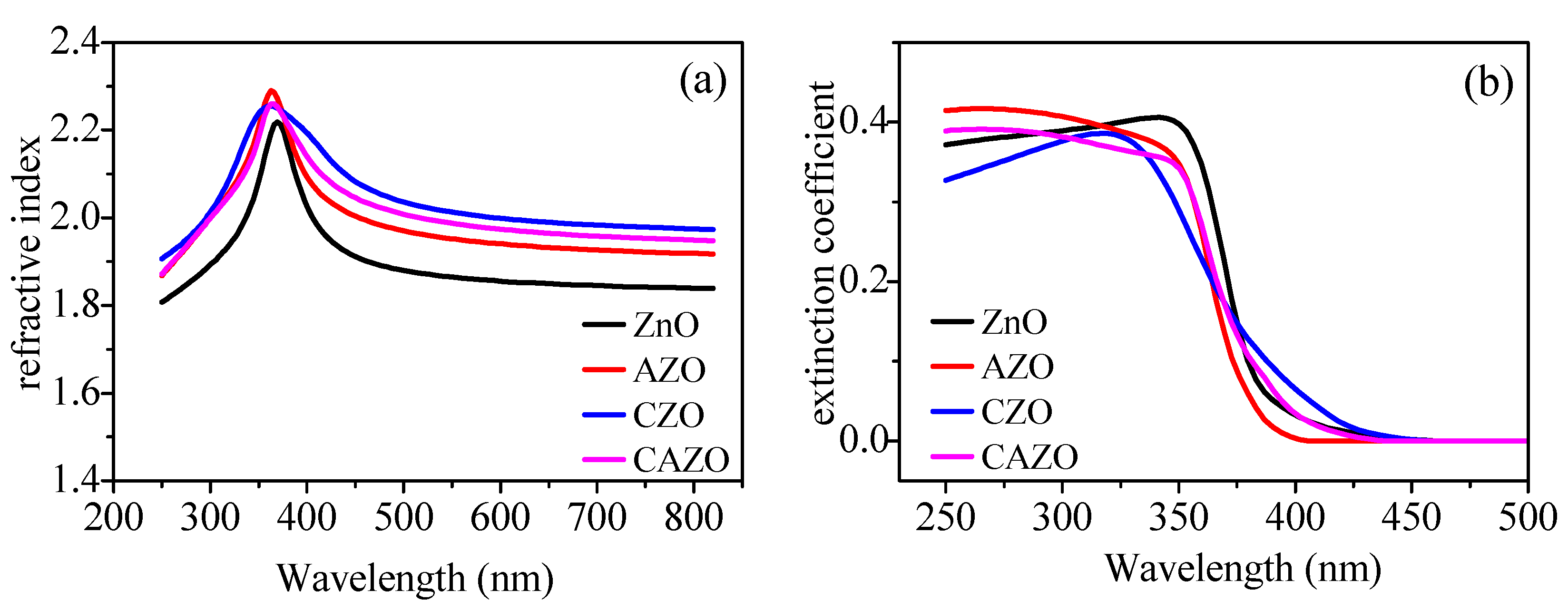
3.3.2. Ellipsometric Measurements

For determination of the refractive index (n), extinction coefficient (k) and film thickness (d), we used ellipsometric measurements and consequent modelling using DeltaPsi2 commercial software, version 2.6 (UVISEL 2, Horiba Jobin Yvon, Longjumeau, France). The measured parameters were the ellipsometric angles Ψ and Δ, defined by Equations (1) and (2):
tan Ψ = r p r s ,   0 o Ψ 90 o
= δ p δ s ,   0 o Δ 360 o
where rp, rs and δp, δs are the amplitudes and phases of reflection coefficients for p- and s-polarized light, respectively, and are functions of the unknown parameters n, k and d. The last were determined by nonlinear minimization of the difference between the measured and calculated ellipsometric angles Ψ and Δ. The Forouhi and Bloomer dispersion equations [38] were applied to express n and k as a function of wavelength, and a three-layered model was implemented for matching the real film. The model comprises a thin (3 nm) native oxide on the silicon substrate, film with unknown parameters (n, k and d) and a top layer with unknown thickness dtop consisting of a 50% volume fraction of voids and a 50% volume fraction of a medium with the unknown parameters n and k. The idea behind the top effective layer is to model the surface roughness of the studied films.
The calculated dispersion curves of the refractive index and extinction coefficient are shown in Figure 6a,b, respectively. The refractive index of all studied films obeys normal dispersion in the visible spectra range, i.e., n decreases with wavelength. This is expected because all films are transparent in this spectral range. It can be seen from Figure 6b that the extinction coefficient is zero for wavelengths longer than 450 nm. The refractive index increases with doping: n for pure ZnO at a wavelength of 600 nm is 1.86 (Table 2), increasing to 2.00 and 1.94 for CZO and AZO films, respectively. For Co/Al-co-doped films, n is 1.97, between the values for CZO and AZO films, as would be expected.
All films have high absorption in the spectral range shorter than 350 nm and strong abnormal dispersion (n increases with wavelength), typical for spectral ranges with high absorption. The fundamental absorption edges of the films are in the spectral range 330–430 nm, and a distinct blue-shift for AZO films compared to pure ZnO is observed. Therefore, an increase in optical band gap for AZO films can be expected. The shift of the absorption edge for CZO and CAZO films is not so clearly distinguished, but there is a very clear change in the slope of the fundamental edge, which is typical for materials with defects and levels in the forbidden band.

3.3.3. Calculation of Optical Band Gap and Urbach Energy

To go deeper inside the absorption behavior of the films, we calculated the optical band gap, Eg, and Urbach energy, EU; the values are presented in Table 2. A Tauc plot [39] was used for calculation of Eg, assuming direct transition between valence and conduction bands. (αE)2 is plotted versus light energy E, and from the linear part of the curve, Eg is calculated at (αE)2 = 0 (α is the absorption coefficient in cm−1, calculated from the previously determined extinction coefficient k, using relation α = 4πk/λ, and E is the photon energy in eV; the power degree is 2 because of the assumption of direct transitions in ZnO). The values of Eg in Table 2 indicate an increase in the optical band gap after doping with 40–60 meV. The widening of the optical band of ZnO after doping with Al and Co has been observed by many authors [10,17,37,40]. The increase in Eg can be attributed to the Burstein–Moss effect, in which the increase in carrier concentration generated from substitution of Zn ions leads to a shift of Fermi level toward the conduction band.
To further clarify the light absorption in the films, we calculated the Urbach energy, EU, which is the width of the band tail (therefore also called the Urbach tail) and is commonly associated with structural disorder in the material. We used the dispersion curve of the extinction coefficient (the absorption coefficient α) in the spectral range, where it obeys exponential decay [39]:
α = α o e x p ( E E U )
where αo is a constant and E is the photon energy in eV. The slope of the linear fit of the plot ln(α) versus E gives the reciprocal value of EU. From Table 2, it can be seen that doping with Co leads to an increase in the Urbach energy to 117 meV for CZO and 19 meV for CAZO films compared to pure ZnO films. This result is expected and explains the observed increase in the slope of the fundamental absorption edge in transmittance spectra (Figure 5) and the tail in extinction spectra for the CZO and CAZO films (Figure 6b). Our results are consistent with the results of other authors. For example, Kaphle and Hari [24] have found that the Urbach energy for CZO films obtained by the chemical bath deposition method increases from 88 meV for pure ZnO to 103 meV and 107 meV for 6% and 9% cobalt-doped films, respectively. Nam et al. [26] have reported an increase in EU from 62 eV for ZnO to 266 eV for 6% Co-doped ZnO films obtained by the sol-gel and spin-coating methods.

4. Conclusions

The successful deposition of Co-doped (CZO) and Co/Al-co-doped (CAZO) ZnO thin films using the electrospray method is demonstrated. All films have granular morphology with homogenous particle distribution on the surface, and no cracks are observed. Cobalt doping leads to a substantial decrease (more than 200%) in grain size from 143 nm in the case of pure ZnO to 61 nm and 71 nm for CZO and CAZO films, respectively, and an increase in crystallite size from 22 nm to 29 nm in the (101) direction. No additional peaks due to dopant impurities or dopant oxides are observed at a 5% doping concentration. All the films are transparent in the visible and near-infrared spectral ranges. The characteristic absorption peaks of Co2+ ions assigned to charge transfers between donor and acceptor ionization levels within the band gap of the ZnO host are clearly distinguishable for both the CZO and CAZO films. The refractive index increases with doping from 1.86 for pure ZnO to 2.00 and 1.97 for CZO and CAZO films, respectively, at a wavelength of 600 nm. A widening of the optical band gap by 40–60 meV after doping is observed and attributed to the Burstein–Moss effect. The structural disorder judged from the calculated Urbach tails is greatest in the CZO films (236 meV), while the values for CAZO and pure ZnO are 138 meV and 119 meV, respectively. High-quality thin films of pure and doped ZnO films with comparable properties to these obtained by other means can be produced using the electrospray method without postdeposition annealing, using nontoxic and inexpensive precursors and solvents. This opens up the possibility of film applications in optoelectronics, spintronics and photocatalysis.

Author Contributions

Conceptualization, G.M. and T.B.; methodology, G.M. and T.B.; software, T.B. and B.G.; validation, G.M., B.G. and T.B.; formal analysis, B.G. and M.V.; investigation, M.V., B.G. and G.M.; resources, G.M. and T.B.; data curation, G.M. and T.B.; writing—original draft preparation, G.M., B.G. and T.B.; writing—review and editing, T.B.; visualization, T.B., B.G. and G.M.; supervision, T.B.; project administration, T.B.; funding acquisition, T.B. All authors have read and agreed to the published version of the manuscript.

Funding

This research was funded by the Bulgarian National Science Fund under the project KП–06–H38/7 (05.12.2019). T.B. and M.V. acknowledge the partial support of the National Center of Mechatronics and Clean Technologies, BG05M2OP001-1.001-0008-C01, supported by the European Regional Development Fund within the Operational Programme “Science and Education for Smart Growth 2014–2020”.

Institutional Review Board Statement

Not applicable.

Informed Consent Statement

Not applicable.

Data Availability Statement

Not applicable.

Acknowledgments

Research equipment of the Distributed Research Infrastructure INFRAMAT, part of the Bulgarian National Roadmap for Research Infrastructures supported by the Bulgarian Ministry of Education and Science, was used in this investigation.

Conflicts of Interest

The authors declare no conflict of interest.

References

  1. Ozgür, Ü.; Alivov, Y.I.; Liu, C.; Teke, A.; Reshchikov, M.A.; Dogan, S.; Avrutin, V.; Cho, S.-J.; Morkoç, H. A comprehensive review of ZnO materials and devices. J. Appl. Phys. 2005, 98, 041301. [Google Scholar] [CrossRef]
  2. Janotti, A.; Van de Walle, C.G. Fundamentals of zinc oxide as a semiconductor. Rep. Prog. Phys. 2009, 72, 126501. [Google Scholar] [CrossRef]
  3. Liu, Y.; Li, Y.; Zeng, H. ZnO-based transparent conductive thin films: Doping, performance, and processing. J. Nanomater. 2013, 2013, 196521. [Google Scholar] [CrossRef]
  4. Poongodi, G.; Anandan, P.; Kumar, R.M.; Jayavel, R. Studies on visible light photocatalytic and antibacterial activities of nanostructured cobalt doped ZnO thin films prepared by sol–gel spin coating method. Spectrochim. Acta A Mol. Biomol. Spectrosc. 2015, 148, 237–243. [Google Scholar] [CrossRef] [PubMed]
  5. Abdelkrim, M.; Guezzoul, M.; Bedrouni, M.; Bouslama, M.; Ouerdane, A.; Kharroubi, B. Effect of slight cobalt incorporation on the chemical, structural, morphological, optoelectronic, and photocatalytic properties of ZnO thin film. J. Alloys Compd. 2022, 920, 165703. [Google Scholar] [CrossRef]
  6. Ali, D.; Butt, M.Z.; Muneer, I.; Farrukh, M.A.; Aftab, M.; Saleem, M.; Bashir, F.; Khan, A.U. Synthesis and characterization of sol-gel derived La and Sm doped ZnO thin films: A solar light photo catalyst for methylene blue. Thin Solid Film. 2019, 679, 86–98. [Google Scholar] [CrossRef]
  7. Liu, W.; Zhou, X.; Xu, L.; Zhu, S.; Yang, S.; Chen, X.; Dong, B.; Bai, X.; Lu, G.; Song, H. Graphene quantum dot-functionalized three-dimensional ordered mesoporous ZnO for acetone detection toward diagnosis of diabetes. Nanoscale 2019, 11, 11496–11504. [Google Scholar] [CrossRef]
  8. Alexieva, G.; Lovchinov, K.; Petrov, M.; Gergova, R.; Tyutyundzhiev, N. Influence of Al Doping on the Morphological, Structural and Gas Sensing Properties of Electrochemically Deposited ZnO Films on Quartz Resonators. Coatings 2022, 12, 81. [Google Scholar] [CrossRef]
  9. Abideen, Z.U.; Kim, J.-H.; Mirzaei, A.; Kim, H.W.; Kim, S.S. Sensing behavior to ppm-level gases and synergistic sensing mechanism in metal-functionalized rGO-loaded ZnO nanofibers. Sens. Actuators B Chem. 2018, 255, 1884–1896. [Google Scholar] [CrossRef]
  10. Rana, S.B.; Singh, R.P.P.; Arya, S. Structural, optical, magnetic and antibacterial study of pure and cobalt doped ZnO nanoparticles. J. Mater. Sci. Mater. Electron. 2017, 28, 2660–2672. [Google Scholar] [CrossRef]
  11. Mahmood, K.; Swain, B.S.; Jung, H.S. Controlling the surface nanostructure of ZnO and Al-doped ZnO thin films using electrostatic spraying for their application in 12% efficient perovskite solar cells. Nanoscale 2014, 6, 9127–9138. [Google Scholar] [CrossRef] [PubMed]
  12. Dietl, T.; Ohno, H.; Matsukura, F.; Cibert, J.; Ferrand, D. Zener model description of ferromagnetism in zinc-blende magnetic semiconductors. Science 2000, 287, 1019–1022. [Google Scholar] [CrossRef] [PubMed]
  13. Lin, H.T.; Chin, T.S.; Shih, J.C.; Lin, S.H.; Hong, T.M.; Huang, R.T.; Chen, F.R.; Kai, J.J. Enhancement of ferromagnetic properties in Zn1−xCoxO by additional Cu doping. Appl. Phys. Lett. 2004, 85, 621–623. [Google Scholar] [CrossRef]
  14. Ueda, K.; Tabota, H.; Kawai, T. Magnetic and electric properties of transition-metal-doped ZnO films. Appl. Phys. Lett. 2001, 79, 988–990. [Google Scholar] [CrossRef]
  15. Lee, H.J.; Jeong, S.Y.; Cho, C.R.; Park, C.H. Study of diluted magnetic semiconductor: Co-doped ZnO. Appl. Phys. Lett. 2002, 81, 4020–4022. [Google Scholar] [CrossRef]
  16. Song, C.; Zeng, F.; Geng, K.W.; Wang, X.B.; Shen, Y.X.; Pan, F. The magnetic properties of Co-doped ZnO diluted magnetic insulator films prepared by direct current reactive magnetron co-sputtering. J. Magn. Magn. Mater. 2007, 309, 25–30. [Google Scholar] [CrossRef]
  17. Chanda, A.; Gupta, S.; Vasundhara, M.; Joshi, S.R.; Mutta, G.R.; Singh, J. Study of structural, optical and magnetic properties of cobalt doped ZnO nanorods. RSC Adv. 2017, 7, 50527–50536. [Google Scholar] [CrossRef]
  18. Paskaleva, A.; Buchkov, K.; Galluzzi, A.; Spassov, D.; Blagoev, B.; Ivanov, T.; Mehandzhiev, V.; Avramova, I.A.; Terzyiska, P.; Tzvetkov, P.; et al. Magneto-Optical and Muliferroic Properties of Transition-Metal (Fe, Co, or Ni)-Doped ZnO Layers Deposited by ALD. ACS Omega 2022, 7, 43306–43315. [Google Scholar] [CrossRef]
  19. Ando, K. Magneto-Optics of Diluted Magnetic Semiconductors: New Materials and Applications. In Magneto-Optics; Sugano, S., Kojima, N., Eds.; Springer Series in Solid-State Sciences; Springer: Berlin/Heidelberg, Germany, 2000; Volume 128, pp. 211–244. [Google Scholar] [CrossRef]
  20. Sutanto, H.; Wibowo, S.; Hadiyanto, H.; Arifin, M.; Hidayanto, E. Photocatalytic activity of cobalt-doped zinc oxide thin film prepared using the spray coating technique. Mater. Res. Express 2017, 4, 076409. [Google Scholar] [CrossRef]
  21. Fitzgerald, C.B.; Venkatesan, M.; Lunney, J.G.; Dorneles, L.S.; Coey, J.M.D. Cobalt-doped ZnO—A room temperature dilute magnetic semiconductor. Appl. Surf. Sci. 2005, 247, 493–496. [Google Scholar] [CrossRef]
  22. Ivill, M.; Pearton, S.J.; Rawal, S.; Leu, L.; Sadik, P.; Das, R.; Hebard, A.F.; Chisholm, M.; Budai, J.D.; Norton, D.P. Structure and magnetism of cobalt-doped ZnO thin films. New J. Phys. 2008, 10, 065002. [Google Scholar] [CrossRef]
  23. Goktas, A.; Aslan, F.; Mutlu, I.H. Effect of preparation technique on the selected characteristics of Zn1−xCoxO nanocrystalline thin films deposited by sol–gel and magnetron sputtering. J. Alloys Compd. 2014, 615, 765–778. [Google Scholar] [CrossRef]
  24. Kaphle, A.; Hari, P. Variation of index of refraction in cobalt doped ZnO nanostructures. J. Appl. Phys. 2017, 122, 165304. [Google Scholar] [CrossRef]
  25. Kaphle, A.; Reed, T.; Apblett, A.; Hari, P. Doping Efficiency in Cobalt-Doped ZnO Nanostructured Materials. J. Nanomater. 2019, 2019, 7034620. [Google Scholar] [CrossRef]
  26. Nam, G.; Yoon, H.; Kim, B.; Lee, D.Y.; Kim, J.S.; Leem, J.Y. Effect of Co doping concentration on structural properties and optical parameters of Co-doped ZnO thin films by sol-gel dip-coating method. J. Nanosci. Nanotechnol. 2014, 14, 8544–8548. [Google Scholar] [CrossRef]
  27. Shukla, P.; Tiwari, S.; Joshi, S.R.; Akshay, V.R.; Vasundhara, M.; Varma, S.; Singh, J.; Chanda, A. Investigation on structural, morphological and optical properties of Co-doped ZnO thin films. Phys. B Condens. Matter 2018, 550, 303–310. [Google Scholar] [CrossRef]
  28. Gungor, E.; Gungor, T.; Caliskan, D.; Ceylan, A.; Ozbay, E. Co doping induced structural and optical properties of sol–gel prepared ZnO thin films. Appl. Surf. Sci. 2014, 318, 309–313. [Google Scholar] [CrossRef]
  29. Yahmadi, B.; Kamoun, O.; Alhalaili, B.; Alleg, S.; Vidu, R.; Kamoun Turki, N. Physical Investigations of (Co, Mn) Co-Doped ZnO Nanocrystalline Films. Nanomaterials 2020, 10, 1507. [Google Scholar] [CrossRef] [PubMed]
  30. Marinov, G.; Lovchinov, K.; Madjarova, V.; Strijkova, V.; Vasileva, M.; Malinowski, N.; Babeva, T. Aluminum-doped zinc oxide thin films deposited by electrospray method. Opt. Mater. 2019, 89, 390–395. [Google Scholar] [CrossRef]
  31. Marinov, G.; Strijkova, V.; Vasileva, M.; Madjarova, V.; Malinowski, N.; Babeva, T. Effect of substrate temperature on the microstructural, morphological, and optical properties of electrosprayed ZnO thin films. Adv. Condens. Matter. Phys. 2018, 2018, 89575077. [Google Scholar] [CrossRef]
  32. El Mir, L.; Ayadi, Z.B.; Saadoun, M.; Djessas, K.; von Bardeleben, H.J.; Alaya, S. Preparation and characterization of n-type conductive (Al, Co) co-doped ZnO thin films deposited by sputtering from aerogel nanopowders. Appl. Surf. Sci. 2007, 254, 570–573. [Google Scholar] [CrossRef]
  33. Ghribi, F.; Khalifi, N.; Mrabet, S.; Ghiloufi, I.; Talu, S.; El Mir, L.M.; Da Fonseca Filho, D.H.; Oliveira, R.M.; Matos, R.S. Evaluation of the structure–micromorphology relationship of Co10%–Alx Co-doped Zinc oxide nanostructured thin films deposited by pulsed laser using XRD and AFM. Arab. J. Sci. Eng. 2022, 47, 7717–7728. [Google Scholar] [CrossRef]
  34. Khan, M.S.; Shi, L.-J.; Zou, B. First principles calculations of optoelectronic and magnetic properties of Co-doped and (Co, Al) co-doped ZnO. J. Appl. Phys. 2020, 127, 065707. [Google Scholar] [CrossRef]
  35. Vempati, S.; Shetty, A.; Dawson, P.; Nanda, K.K.; Krupanidhi, S.B. Solution-based synthesis of cobalt-doped ZnO thin films. Thin Solid Film. 2012, 524, 137–143. [Google Scholar] [CrossRef]
  36. Nakrela, A.; Benramdane, N.; Bouzidi, A.; Kebbab, Z.; Medles, M.; Mathieu, C. Site location of Al-dopant in ZnO lattice by exploiting the structural and optical characterisation of ZnO:Al thin films. Results Phys. 2016, 6, 133–138. [Google Scholar] [CrossRef]
  37. Yoo, Y.-Z.; Fukumura, T.; Jin, Z.; Hasegawa, K.; Kawasaki, M.; Ahmet, P.; Chikyow, T.; Koinuma, H. ZnO–CoO solid solution thin films. J. Appl. Phys. 2001, 90, 4246–4250. [Google Scholar] [CrossRef]
  38. Forouhi, A.R.; Bloomer, I. Optical properties of crystalline semiconductors and dielectrics. Phys. Rev. B 1988, 38, 1865–1874. [Google Scholar] [CrossRef]
  39. Tauc, J.; Menth, A. States in the gap. J. Non-Cryst. Sol. 1972, 8–10, 569–585. [Google Scholar] [CrossRef]
  40. Fang, D.; Lin, K.; Xue, T.; Cui, C.; Chen, X.; Yao, P.; Li, H. Influence of Al doping on structural and optical properties of Mg–Al co-doped ZnO thin films prepared by sol–gel method. J. Alloys Compd. 2014, 589, 346–352. [Google Scholar] [CrossRef]
Figure 1. Scheme for electrospray deposition of thin films: 1—syringe pump, 2—syringe with ZnO precursors, 3—emitter, 4—collector, 5—high voltage power supply, 6—controllers for motors and temperature.
Applsci 13 09611 g001
Figure 2. SEM pictures of pure ZnO thin films (a) and films doped with 5% of Al (b), 5% of Co (c) and co-doped with 5% of Al and Co (d). The scale bar is 1 μm.
Applsci 13 09611 g002
Figure 3. XRD patterns of pure ZnO films and films doped with 5% Al (AZO), 5% Co (CZO) and co-doped with 5% of Al and Co (CAZO).
Applsci 13 09611 g003
Figure 4. TEM pictures of pure ZnO films (a) and films doped with 5% Al (AZO) (b), 5% Co (CZO) (c) and co-doped with 5% of Al/Co (CAZO) (d). The typical SAED pattern with indexed diffraction is displayed as an inset.
Applsci 13 09611 g004
Figure 5. Transmittance spectra of pure ZnO thin film and ZnO doped with Al (AZO), Co (CZO) and (Co/Al) (CAZO) with a concentration of 5%.
Applsci 13 09611 g005
Figure 6. Refractive index (a) and extinction coefficient (b) of pure ZnO (black line) and ZnO doped with Al (AZO) (red line), Co (CZO) (blue line) and Co/Al (CAZO) (magenta line) measured ellipsometrically.
Applsci 13 09611 g006
Table 1. Average grain size with standard deviations measured from SEM pictures (Figure 2) and calculated crystallite size D in indicated crystallographic planes.
SampleGrain Size (nm)D100 (nm)D002 (nm)D101 (nm)
ZnO143 ± 34262122
AZO128 ± 23251918
CZO62 ± 10222029
CAZO71 ± 10262122
Table 2. Surface roughness in nm, refractive index n at wavelength of 600 nm, direct optical band gap Eg in eV and Urbach energy EU in meV.
Samplerms Roughness (nm)n @ 600 nmEg (eV)EU (meV)
ZnO261.863.29119
AZO341.943.35110
CZO312.003.35236
CAZO351.973.33138
Disclaimer/Publisher’s Note: The statements, opinions and data contained in all publications are solely those of the individual author(s) and contributor(s) and not of MDPI and/or the editor(s). MDPI and/or the editor(s) disclaim responsibility for any injury to people or property resulting from any ideas, methods, instructions or products referred to in the content.

