Article

High-Aspect-Ratio Silicon Metasurfaces: Design, Fabrication, and Characterization

1
State Key Laboratory of Surface Physics, Key Laboratory of Micro and Nano Photonic Structures (Ministry of Education) and Department of Physics, Fudan University, Shanghai 200433, China
2
Shanghai Engineering Research Centre of Ultra Precision Optical Manufacturing, Department of Optical Science and Engineering, School of Information Science and Technology, Fudan University, Shanghai 200433, China
*
Author to whom correspondence should be addressed.
Appl. Sci. 2023, 13(17), 9607; https://doi.org/10.3390/app13179607
Submission received: 18 July 2023 / Revised: 12 August 2023 / Accepted: 14 August 2023 / Published: 24 August 2023
(This article belongs to the Special Issue Terahertz Technologies and Applications)

Abstract

:
Unrestricted manipulations on terahertz (THz) waves are highly desired in integration-optics, but THz devices based on conventional materials are usually bulky in size. Although all-silicon metasurfaces have exhibited great capabilities in manipulating THz waves, most of them are less efficient and have limited functionalities. In this work, we first design a silicon meta-atom structure consisting of a high-aspect-ratio (AR) micro-pillar that exhibits nearly perfect transmission and large transmission phase of THz wave, and systemically study how the fabrication quality (e.g., steepness of the sidewall and the vertical thickness distribution) may influence the final performance of a functional metasurface constructed with such meta-atoms. After experimentally examining how two working phases in the deep-reactive-ion-etch technology (i.e., the etch and passivation phases) influence the quality of the fabricated meta-devices, we develop an optimized Bosch process to realize high-AR (~20:1) all-silicon metasurfaces by balancing two working phases. We finally design/fabricate a high-AR silicon metasurface and experimentally demonstrate that it behaves as a high-efficiency half-wave-plate for THz waves in transmission geometry. Our results pave the avenue to realize ultra-compact THz meta-devices with high performance in transmission geometry, which is highly desirable for THz applications.

1. Introduction

The arbitrary control on a terahertz (THz) wave is highly desired due to tremendous application demands, such as biological sensing, security, information communications, etc. However, traditional THz devices usually suffer from issues such as low working efficiency, bulky sizes, limited wave-control functionalities and difficulties for optics integration. The inherent reasons are due to the weak interactions between THz waves and their weak interaction with naturally existing materials, which exhibit limited variation range in permittivity and permeability.
Metasurfaces, 2D metamaterials constructed from planar subwavelength units (e.g., meta-atoms) with pre-designed electromagnetic (EM) responses globally arranged in certain sequences, have attracted immense research interest due to their strong capabilities in manipulate EM waves at different wavelength ranges. Many fascinating wave-manipulation effects have been demonstrated with metasurfaces exhibiting certain phase distributions [1,2], such as anomalous deflection [3], conversion from propagating waves to surface waves [4], meta-holograms [5,6], meta-lens imaging [7,8,9], polarization manipulation [10,11,12] and many others [13,14,15,16,17,18,19,20]. Metasurfaces were also proposed as ultra-thin and efficient THz devices, such as wave-plates [21], meta-lenses [13,22], beam deflectors [23], THz special beam generators [24,25] and so on [26]. However, THz meta-devices made from metals are usually of limited working efficiencies due to inevitable metallic losses. To overcome such an issue, researchers proposed to use low-loss dielectric materials to construct metasurfaces, and realized many high-efficiency meta-devices in different frequency regimes [7,8,14,15,27]. Some high-efficiency polarization controls of propagation wave, plane waves and guided waves [10,11,12] have been achieved with all-dielectric metasurfaces. At THz frequencies, silicon has been considered as an ideal material to construct meta-devices, thanks to its low-loss properties and mature COMS fabrication technology.
Through reviewing the performances of silicon meta-surfaces realized so far in the THz regime [17,24,28,29,30,31,32,33,34,35,36,37,38], most of them still suffer from the issues of low working efficiency and narrow working bandwidth, especially for transmissive meta-devices. The inherent reasons are that the adopted meta-atoms are usually not well designed since an optimized design is difficult to realize due to restrictions on sample fabrication. As discussed in our recent work [39], in order to realize the desired wave-front manipulation on THz waves, each meta-atom should exhibit a wave-range of phase modulation and a high transmission efficiency simultaneously, which requires that the constitutional silicon meta-atom should possess a high aspect-ratio (AR) and a good fabrication quality. Unfortunately, making such high-quality silicon meta-structures is challenging with current fabrication technologies.
Here, we develop a fabrication technology to realize high-performance silicon meta-devices for controlling THz waves with diversified functionalities. We first design a silicon meta-atom consisting of a high-AR micro-pillar (see Figure 1a), and then systematically study how the fabrication quality can affect the final performance of a meta-device constructed from such meta-atoms. We next examine how two crucial steps in deep-reactive-ion-etch (DRIE) technology [40,41,42] (i.e., the etch phase and the passivation phase) influence the quality of the fabricated structure, based on which we develop an optimized Bosch process to fabricate silicon meta-devices with the best qualities by balancing the two working phases. Finally, we employ the developed Bosch process to fabricate a silicon THz meta-device with an AR of 12:1, and experimentally characterize its polarization-control performance.

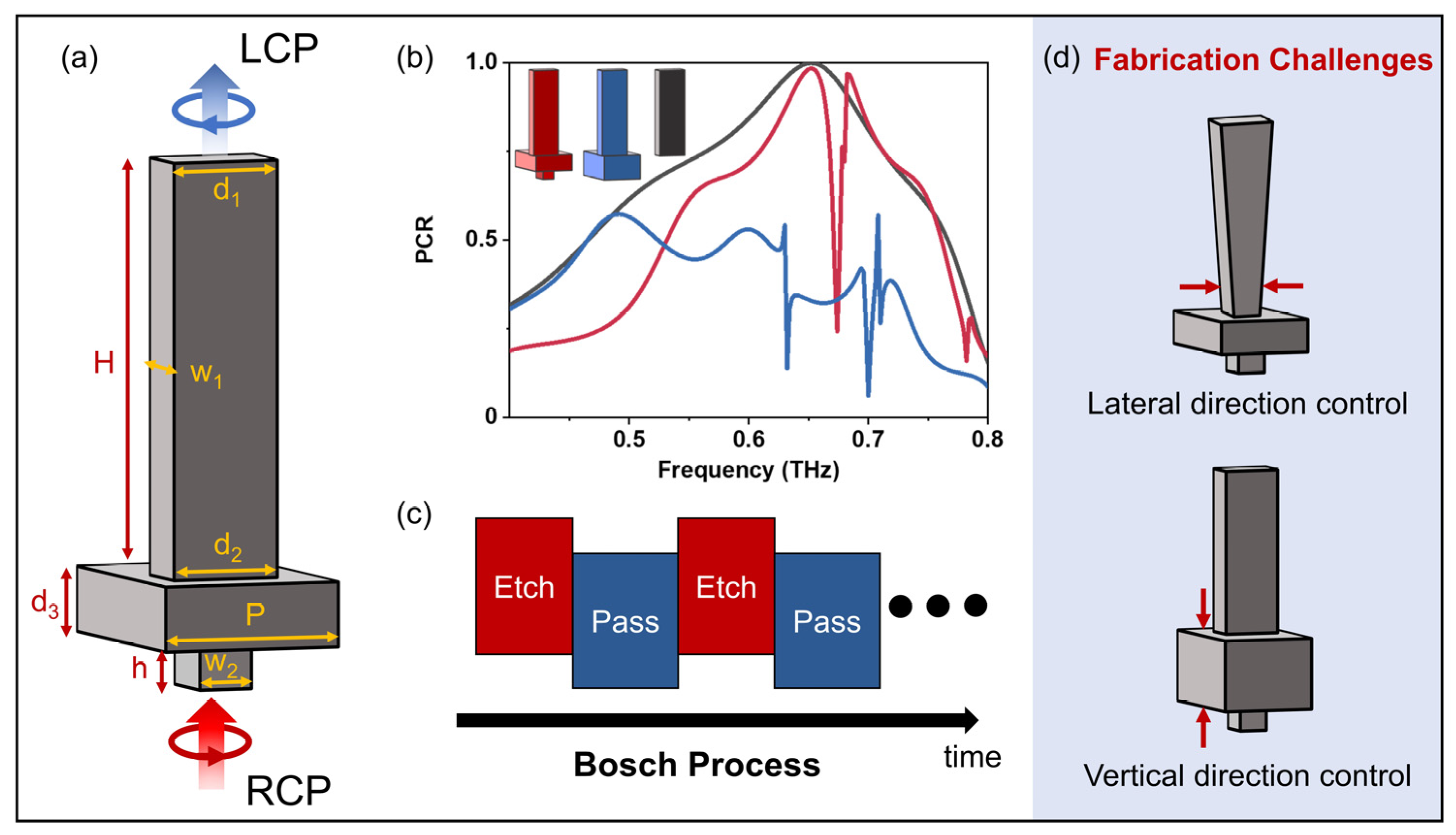
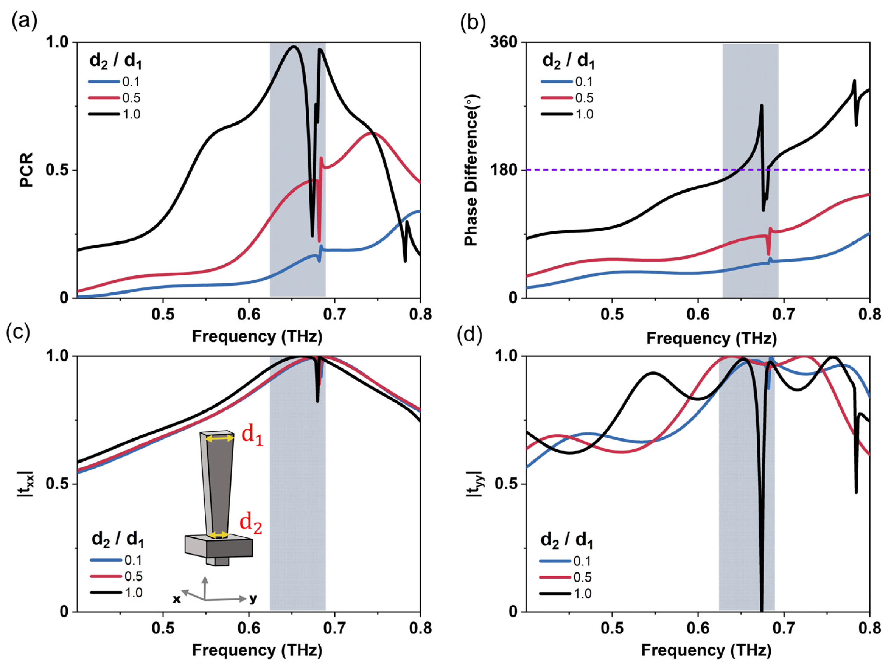
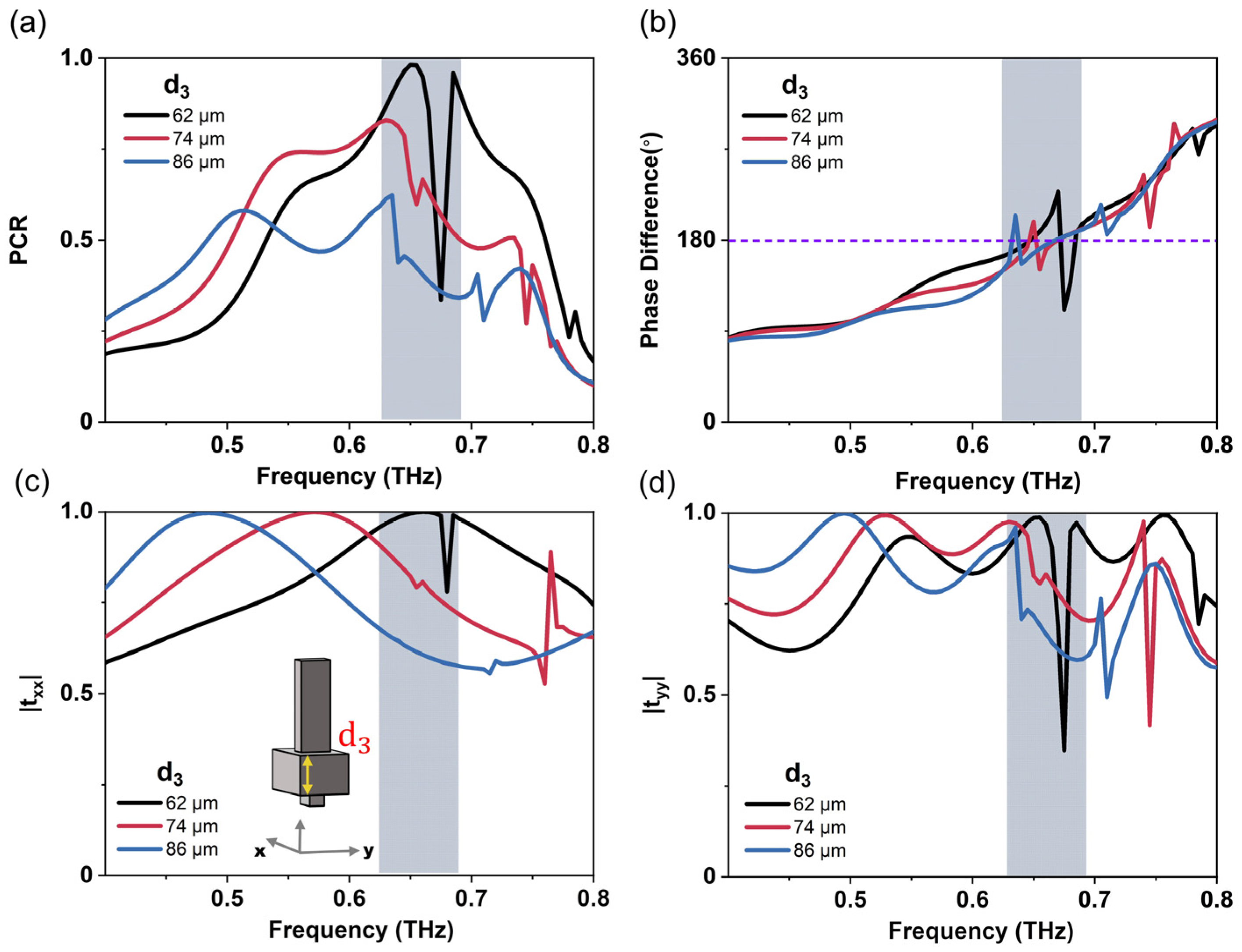
2. Design of the Transmissive Silicon Meta-Atom

We start by presenting how to design the transmissive THz silicon meta-atom exhibiting high transmittance, a high polarization conversion ratio and a transmission phase covering a sufficiently large range, which can be the basic element to construct performant metasurfaces with different functionalities [17,24,28,29,30,31,32,33,34,35,36,37,38]. Although silicon structures using Mie resonances can manipulate the transmission amplitude and phase [43,44,45,46], it is very difficult to achieve these requirements simultaneously with low-AR silicon design. As demonstrated in our recent work [39], though the silicon pillar structure with high AR can well achieve the above-mentioned demand, it is impossible to fabricate it in free-standing geometry. In practice, the micro-pillar should be deposited or etched on a substrate, and the presence of a substrate will dramatically modify the performance of the free-standing meta-atoms design. To clarify this point, we perform a full-wave simulation to demonstrate the polarization conversion effect of free-standing meta-atoms and the micro-pillar with a substrate, which are arranged in a square lattice with a periodicity of 157 μm (with following geometrical parameters: H = 400 , h = 30 , d 1 = d 2 = 132 , w 1 = 33 , w 2 = 50 ,   d 3 = 62 , all in units of μm). Here, we take the meta-half-wave-plate (MHWP) design as an example. As shown in Figure 1b, the metasurface composed of the free-standing micro-pillars can function well as a half-wave-plate (HWP) with a polarization conversion ratio (PCR) (PCR= t x x t y y 2 / 4 , where t x x and t y y denote the complex transmission coefficients for the x- and y-polarized waves) near to 1 at a working frequency of 0.65 THz, where all the input power of the incident right circular polarized (RCP) THz wave can be fully converted into the left circular polarized (LCP) component. Actually, the presence of the substrate largely modifies the PCR performance of the ideal free-standing MHWP, as illustrated by the blue line in Figure 1b, which was associated with the additional reflection induced by the impedance mismatch at the interface of the substrate and air. To compensate such an effect, the carefully designed silicon micro-resonators are added to another side of the substrate as an anti-reflection layer, which can efficiently reduce the reflections induced by the substrate. Consequently, as shown in Figure 1a, our proposed meta-atom consists of three silicon layers, including a 400 μm high micro-pillar with a rectangular cross-section, a 62 μm thick continuous substrate and a 30 μm high micro-resonator with optimized dimensions to obtain high transmission for the whole meta-atom design at the desired working frequency. One can see that our tri-layered meta-atom design exhibits almost perfect HWP performance at 0.65 THz and a working bandwidth of about 0.1 THz. It is worth mentioning that by changing the geometrical parameters of a tri-layered meta-atom with high AR, one can realize many different functionalities, with high transmittance and large transmissive phase coverage, such as meta-lens and beam deflectors.
In practice, the fabrication of tri-layered all-silicon metasurfaces with such high AR can technically be carried out by conversional photolithography and plasma etching in the Bosch process with an altering multi-stepped etch cycle and passivation cycle [40,41,42], as shown in Figure 1c. However, it is quite difficult to achieve the perfect etching control in both the lateral and vertical direction for dielectric metasurfaces with high AR, which will determine the sidewall profile and vertical thickness distribution (VTD) (i.e., especially for the thickness of continuous substrate), respectively, as illustrated in Figure 1d.
We now illustrate how the structural effects, including the sidewall profile and thickness of the continuous substrate, affect the performance of our designed MHWP, numerically calculating the transmittance and transmission phase with a Finite Difference Time Domain (FDTD) simulation. In our simulations, the refractive index of silicon is set as n S i = 3.45 . The simulated results in Figure 2 illustrate the influence of the sidewall profile on the performance of the designed MHWP with three typical cases. Here, we only consider the sidewall profile in one direction, defined as the ratio between the bottom width (d2) and the top width (d1) of the micro-pillar, with all other parameters fixed as the designed ones (see the inset in Figure 2c). The designed meta-atom has a straight sidewall profile with d2/d1 = 1, as shown in Figure 1a. Usually, the sidewall slope will decrease with the d2/d1 due to the imperfect lateral control of the DRIE fabrication process. The simulation results shown in Figure 2a illustrate that the PCR of the designed MHWP will significantly decline with the decrease in d2/d1. Here, the simulated spectra of the PCR were obtained by calculating the power ratio between the LCP transmitted THz wave and the incident RCP THz wave based on the FDTD simulation. The simulated transmission amplitude spectra along the x and y direction shown in Figure 2c,d illustrate that the sidewall slope slightly influences the transmission of the meta-atom. Meanwhile, it did largely modify the phase difference between two crossed-polarized THz waves, as shown in Figure 2b. In particular, the phase difference changed from 180° to 90° and to 45° for these three cases, respectively. The underlying physics of this effect is related to the anisotropic design of the micro-pillar with rectangular shape. The sidewall profile reduces the effective refractive index of the silicon pillar at different vertical positions, making the meta-atom exhibit less anisotropic properties, which results in the decrease in the phase difference of the two cross-polarized transmitted THz wave. In addition, the pronounced dip in the spectra of the PCR origins from a Fabry–Perot resonance of the anti-reflection layer, which can be remedied by optimizing the geometrical parameter of the micro-resonators, or shifted away from the working bandwidth of our device by changing the periodicity of the structure, as shown in the Supplementary Materials.
To illustrate the influence of the connecting layer thickness on the performance of the MHWP, we perform a similar FDTD simulation with three different thickness of the connecting silicon layer d3(see the inset to Figure 3c). Here, all the parameter of the tri-layered meta-atom are fixed, except the height of the micro-pillar determined by H = 400 − d3. As can be seen in Figure 3a, d3 can significantly affect the polarization conversion performance of the designed MHWP. The simulated results plotted in Figure 3b illustrate that the imperfect thickness control on d3 slightly affects the phase difference between the two linearly cross-polarized THz waves, since the VTD almost did not influence the anisotropy property of the micro-pillar design with a straight sidewall. Meanwhile, the variation in the VTD of the meta-atom will lead to a frequency shift of the prefect transmittance for both the x- and y-polarized THz waves, as shown in Figure 3c,d, respectively. The underlying physics of such a phenomenon might be the mode mismatch between the resonant design for the anti-reflection layer and the structure of the modified two top layers. Consequently, it is not surprising to find the performance decay of the MHWP, since the PCR is strongly dependent on the transmittance for two co-polarized THz waves.
Actually, the sidewall slope and the incorrect VTD of the meta-atom might happen at the same time in the real fabrication process, resulting in a more complex effect on the performance of meta-devices. In addition, the micro-grass effect in silicon etching should also be seriously considered to realize the correct VTD control [47,48]. Thus, it is important to find the correct fabrication receipt to realize the ideal tri-layered meta-atom with high AR, straight sidewall and correct VTD. It is worth emphasizing that our design strategy is applicable to realize different high-efficient dielectric meta-atoms with large transmissive phase coverage at different working frequency regimes, which can form the ideal building blocks to design transmissive meta-devices with different functionalities, such as multifunctional wave-front control, vectoral beam generations [49,50], and so on.

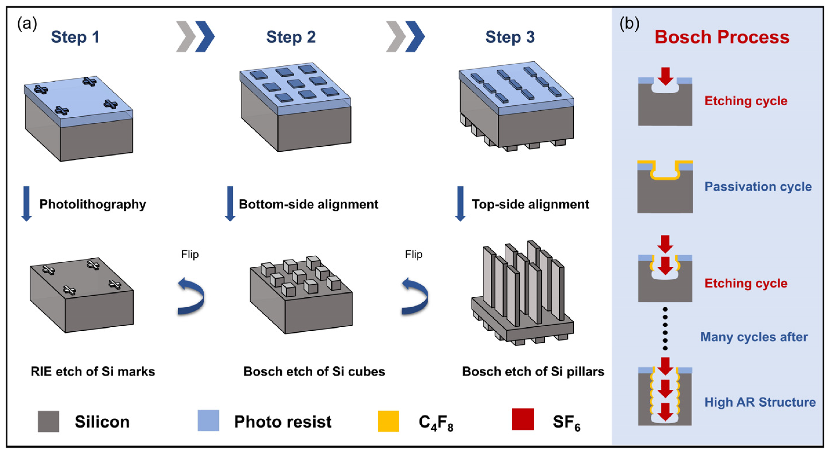
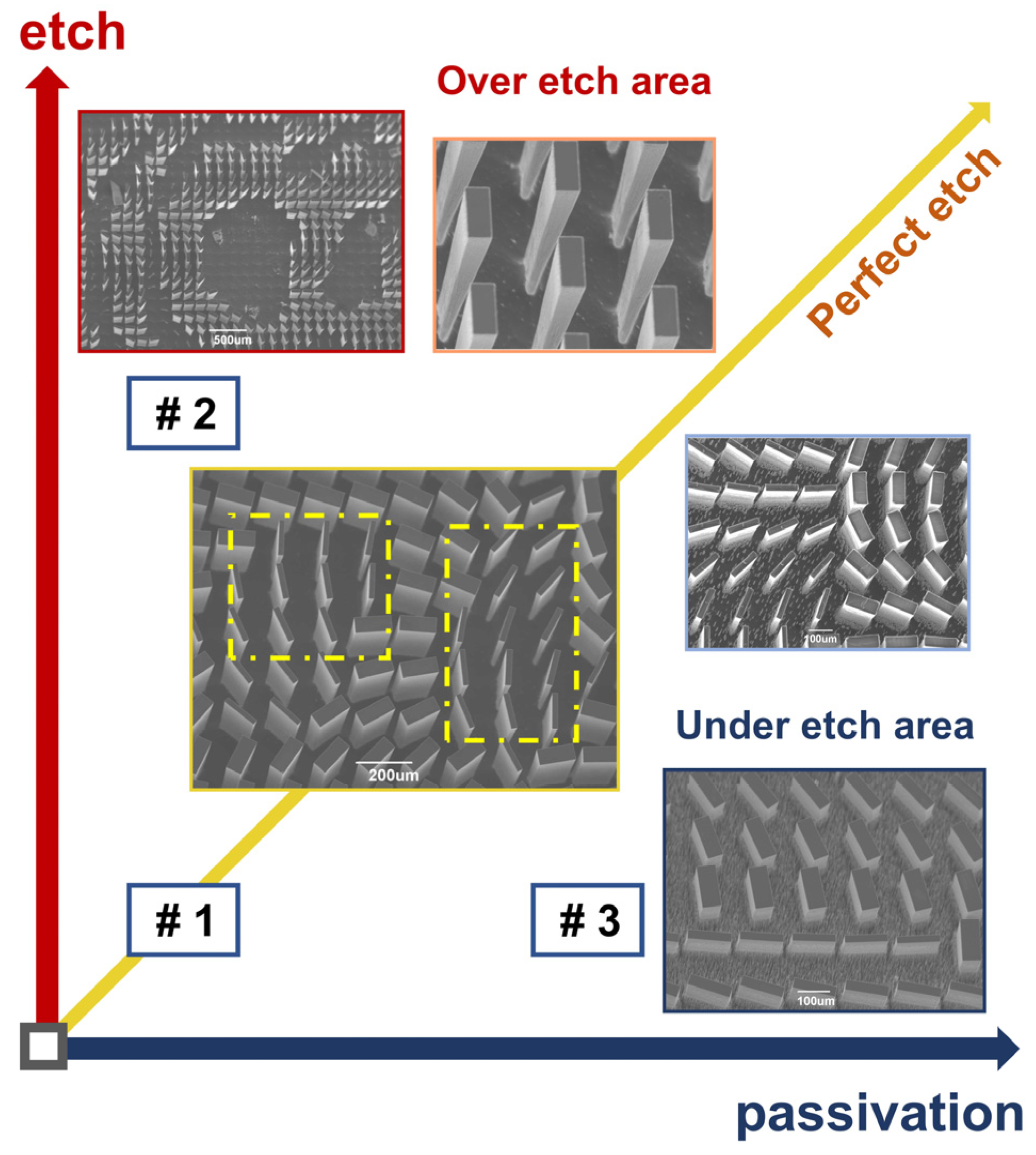
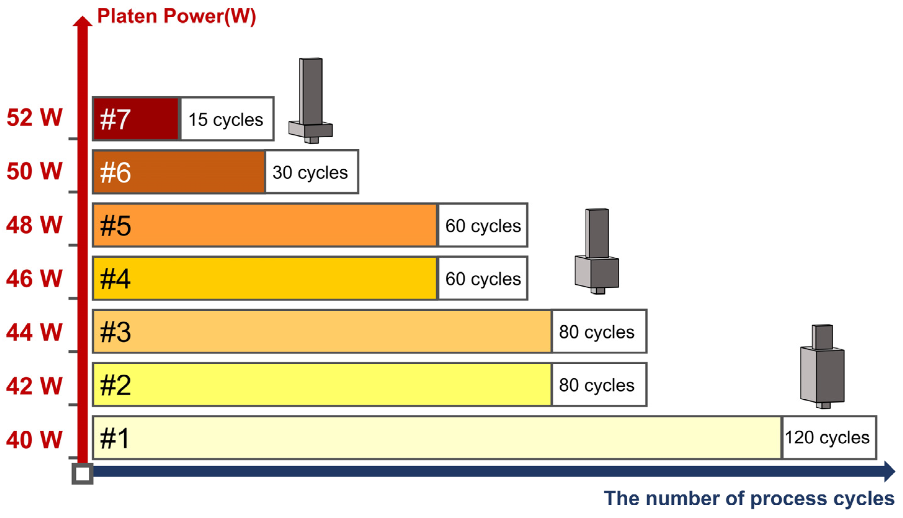
3. Fabrication Process for High-AR Silicon Metasurfaces

The fabrication of the tri-layered all-silicon THz metasurfaces, with a straight sidewall and correct VTD, was carried out with a three-step process based on standard photolithography and the Bosch silicon etch process, as shown in Figure 4a. Firstly, a spin-coating photoresist (PR) layer (AZ5214) is covered and patterned on the top side of the double-sided polished (DSP) silicon wafer with a thickness of 500 μm. A set of cross-shaped silicon marks is transferred onto the silicon wafer using the standard RIE process. Next, the pattern of silicon micro-resonators is transferred onto the bottom side of the silicon wafer, making good alignment with the help of the cross-shaped marks on the top side of the wafer. Then, the silicon resonators with a height of 30 μm on the bottom side of the wafer are realized by utilizing the Bosch etching process with the advanced silicon etcher (Surface Technology System, MUC-21). In the third step, after making good alignment with both the top and bottom structure, we transfer the patterns of the micro-pillar onto the thick PR (AZ 4620) covered with a wafer for protection. Finally, the high-AR silicon micro-pillar array on the top side of the wafer is carried out with another optimized Bosch etch process.
As shown in Figure 4b, the Bosch process is a time-multiplexed silicon etching procedure consisting of multiple switches between the etching cycle and the passivation cycle [40,41,42] to guarantee a highly directional etch. In the passivation active cycle, a thin film of fluorocarbon, also called the inhibitor, is deposited all over the structures. In the following etch-active cycle, the reactant will first remove the inhibitor, then etch the silicon in depth. In return, the etch rate in the horizontal direction is dramatically different from the vertical direction, since the sidewall of the silicon has been well protected by the inhibitor. Therefore, the anisotropic etch in the vertical and lateral directions in the silicon substrate can be realized by switching these two cycles in time.
In the Bosch process, side effect control is the key technique to promoting the etch profile. Usually, when the balance between etch step and passivation step is disturbed, the side effects occur [51]. We perform different fabrication processes to find the influence of fabrication setting parameters on the etch profile of a fabricated sample. The comparison experiments on different fabrication parameters, as shown in Figure S1 in Supplementary Materials, shows that the sidewall slope will decrease with the increase in the platen power, because the platen can accelerate the reactant ion to enhance the lateral etch. Although, adjusting the platen power can make the high-AR micro-pillar with a straight sidewall slope, it also risks inducing the presence of a micro-grass effect on the bottom of the silicon substrate. By gradually increasing the passivation active time in each cycle, we find that the long passivation time can enhance the micro-masking, which will also induce a micro-grass effect. Figure S1 illustrates that the etch rate will drop with the increasing passivation in the whole working cycle, because the overdosed residual inhibitor will slow down the etching reaction on the bottom side of the substrate and make the etch reaction more difficult.
To the best of our knowledge, the experimentally realized THz silicon metasurfaces reported in recent literature possessed an etch depth of barely larger than 200 μm with AR values larger than 10:1 [17,24,28,29,30,31,32,33,34,35,36,37,38]. This is due to the difficulty to control the sidewall effect related to the etching process, especially for cases with high AR. In the Bosch process, the etch and passivation steps not only cooperate with each other but also compete against each other. The different combination of etch and passivation will lead to very different sidewall effects, thus finding the balanced state between these two steps is crucial to achieve the high-AR silicon etch [51].
As shown in Figure 5, if the passivation step continuously suppresses the etch one, the reactant cannot sufficiently react with the inhibitor, leaving residue on the bottom of the silicon to form micro-masking [48]. The roughness of the bottom surface of the substrate will be enhanced after multiplex working cycles, resulting in the presence of micro-grass on the bottom [47]. Such an effect, also known as the black silicon effect, can be readily illustrated with case #3 shown in Figure 5.
On the other hand, when the etch step suppresses the passivation step, the reactant will exhaust the inhibitor on the surface of the etched structures, and eventually lead to an isotropic etch in the vertical and lateral directions. In this case, the inhibitor on the sidewall will first be removed, and the sidewall of the structure will be etched, resulting in lateral etching. As the time-multiplexed process proceeds, the undercut of the bottom region of the structure will move further in the lateral direction of the pillar, and finally lead to the sidewall slope, even collapsing the micro-pillars, as shown with case #2 in Figure 5.
Fortunately, once the balance between the etch and passivation cycles has been found, the perfect high-AR silicon etch can be achieved as shown with case #1 in Figure 5. In particular, our fabricated MHWP is of an AR of 20:1 (as show by the yellow dashed line area in the SEM image; the width of the fabricated micro-pillar is about 20 μm) and the height of pillar of 400 μm. After optimization of the etch profile by finding the balanced process, we still need to precisely control the etch depth which directly affects the VTD of our tri-layered meta-device. Notice that the presence of the silicon cubes on the bottom side of the silicon wafer will induce non-uniform heat distribution on the bottom side of the wafer, which might lead to a non-uniform etch rate at the bottom side of the structures or causes a micro-grass effect. In order to avoid such negative influences, we adopt a gradient parameter recipe consisting of different processing cycles and platen power in multistage steps, to maintain the balanced state for high-AR silicon etching, as shown in Figure 6. At the beginning of the etching process, the structure is well protected by the thick PR; thus, we apply the etch recipe with a great number of working cycles and a low platen power to increase the etch efficiency and lower the damage to the PR from the reactant. With the increase in the etching depth, the etch rate drops significantly, since it become more difficult for the reactants to reach the bottom of the structure. We increase the platen power, providing a directional accelerating electric field, to maintain the etch profile balance. The increased platen power can also increase the temperature of the substrate and PR, thus increasing the etch rate of the PR. To compensate such an effect and provide better control over the etch depth, we reduce the number of working cycles to lower the substrate temperature. Finally, we established an optimized multi-stepped etching process with a gradual decrease in the number of working cycles and a gradual increase in platen power to fabricate tri-layered meta-devices with HAR, as shown in Figure 6.
In this subsection, we demonstrate the importance of the balance between the etch and passivation in the etching process to obtain the straight sidewall profile, and we proposed a multi-stepped etching process with adjusted working cycles and platen power to help us control the quality of the fabricated silicon metasurfaces in both the lateral and vertical directions. It is worth noting that our proposed fabrication techniques can be applicable to realize dielectric metasurfaces working at infrared even visible regimes with smaller etch feature sizes. Recently, the cryogenic reactive ion etching techniques [52] and modified three-step Bosch process [53] have been adopted to achieve the silicon structures with an AR reaching to 50:1 [54].

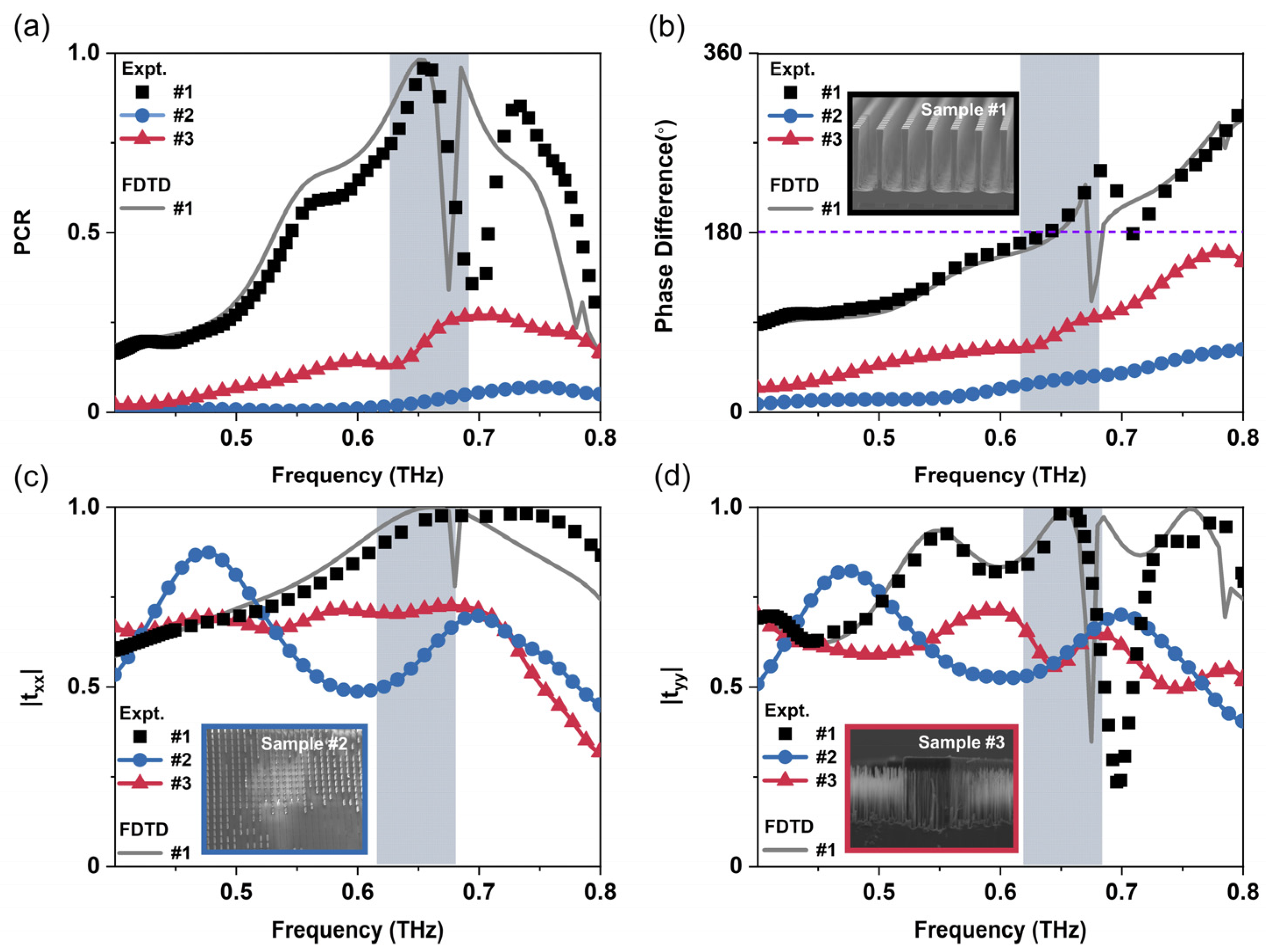
4. Optical Characterization

We utilize THz time-domain spectroscopy (TDS) to characterize the polarization conversion performance of the fabricated samples of different quality to demonstrate the importance of the meta-atom design and the fabrication method. We evaluate the PCR by measuring the transmission amplitude and phase with x- and y-polarized incident THz waves, respectively. Here, we take the transmission amplitude through a fixed aperture without a sample as the reference signal for both polarizations. Figure 7b–d present the measured spectra of the transmission amplitude for x- and y-polarized waves and phase difference between two cross-polarized waves for the three samples with different fabrication quality. The SEM images of these fabricated samples are presented by the insets in Figure 7b–d, with the etch profiles shown by cases #1–3 shown in Figure 5. As shown in Figure 7a, the PCR of sample #1 with a straight sidewall (i.e., aspect ratio (AR) is about 12:1) and a correct vertical thickness distribution, nearly reach 100% at the working frequency of 0.65 THz. Here, we can readily find that our experimental and simulation results are in good agreement for the sample #1 with good fabrication quality. At the working frequency of 0.69 THz, the low PCR caused by resonance can be remedied by optimizing the geometrical parameter of the micro-resonators. The discrepancy between the experimental and simulation results on the Q-factor of resonance at ~0.67 THz might be related to the fabrication imperfection of our device, including the imperfect thickness control of the micro-pillar and connecting layers or/and the etch profile of the micro-pillar. In addition, the working bandwidth of our MHWP can be further improved by carefully designing the periodicity of the structure (see Figure S2 in Supplementary Materials).
In contrast, sample #3 without precise quality control on the VTD exhibits very poor polarization conversion capabilities with a PCR of ~25%, as shown by the red tri-angles in Figure 7a. From the measured spectra shown in Figure 7b–d, one can notice the phase difference between the x- and y-polarized transmitted THz waves decrease to 90°, and the transmission amplitude for both polarizations also drops significantly at the designed working frequency. The main reason might be related to the distorted anisotropy properties of meta-atoms, due to the presence the micro-grass effect, as illustrate by the inset in Figure 7d.
Due to the serious sidewall slope issue for sample #2 (e.g., inverted cone shape or collapse of the micro-pillars), its anisotropic property can be completely ruined (see the inset in Figure 7c). The blue dotted lines in Figure 7b–d illustrate that the measured transmission amplitude spectra for x- and y-polarized THz waves are of similar line shape, and the phase difference between the two crossed-polarizations is only about 20°. Both facts illustrate that the serious sidewall slope issue almost totally destroys the anisotropic property of the designed meta-atom. Here, since the presence of the micro-grass effect and the sidewall slope issue are too complex to numerically simulated, we cannot compare the experimental results with the simulated ones for samples #2 and #3.
From our optical characterization, it can be concluded that our tri-layered silicon meta-atom design is an ideal candidate to design transmissive THz meta-devices, which simultaneously exhibit high transmittance with a large enough transmission phase coverage. Additionally, the adopted fabrication methods, especially the balanced etching process, can help to realize silicon metasurfaces with high AR.

5. Conclusions

In this paper, we propose a fabrication technology with an optimized Bosch process to realize high-performance silicon meta-atoms in a THz regime with different functionalities in transmission geometry. We first designed the high-performance meta-atom consisting of high-aspect-ratio (AR) micro-pillars and systematically demonstrated the influence of fabrication quality on the final performance of the designed meta-device serving as a THz meta-half-wave-plate. After demonstrating the importance of finding a proper Bosch process with balanced working phases, we successfully fabricated a meta-device consisting of high-AR meta-atoms, 400 μm in etch depth and a high aspect ratio of 20:1, by employing the optimized Bosch process with a gradient parameter recipe. At last, we conducted experimental characterization of the polarization-control performance for the designed meta-device. Our findings not only provide a design concept to realize ultra-compact THz meta-devices with high-performance transmission geometry, but also improve the Bosch process to fabricated high-AR micro-structures, paving the avenue for future THz meta-devices for applications in bio-sensing, tele-communication and so on.

Supplementary Materials

The following supporting information can be downloaded at: https://www.mdpi.com/article/10.3390/app13179607/s1, Figure S1: Influence of parameters on the fabrication quality of silicon metasurfaces; Figure S2: Optimized broadband meta-half-wave plate.

Author Contributions

Fabrication, simulation and experimental characterization, Y.Y.; experimental characterization, Z.W.; fabrication, Z.Z. and Y.H.; writing—review and editing, Y.Y., S.S., Q.H. and L.Z. All authors have read and agreed to the published version of the manuscript.

Funding

This work was financially supported by the following projects: National Key Research and Development Program of China (No. 2022YFA1400200), National Natural Science Foundation of China (No. 11734007, No. 12221004, No. 62192771), Natural Science Foundation of Shanghai (No. 20JC1414601), and China Postdoctoral Science Foundation 2021TQ0077.

Institutional Review Board Statement

Not applicable.

Informed Consent Statement

Not applicable.

Data Availability Statement

Not applicable.

Conflicts of Interest

The authors declare no conflict of interest.

References

  1. Chen, H.T.; Taylor, A.J.; Yu, N. A review of metasurfaces: Physics and applications. Rep. Prog. Phys. 2016, 79, 076401. [Google Scholar] [CrossRef] [PubMed]
  2. He, Q.; Sun, S.; Xiao, S.; Zhou, L. High-Efficiency Metasurfaces: Principles, Realizations, and Applications. Adv. Opt. Mater. 2018, 6, 1800415. [Google Scholar] [CrossRef]
  3. Yu, N.; Genevet, P.; Kats, M.A.; Aieta, F.; Tetienne, J.-P.; Capasso, F.; Gaburro, Z. Light propagation with phase discontinuities: Generalized laws of reflection and refraction. Science 2011, 334, 333–337. [Google Scholar] [CrossRef] [PubMed]
  4. Sun, S.; He, Q.; Xiao, S.; Xu, Q.; Li, X.; Zhou, L. Gradient-index meta-surfaces as a bridge linking propagating waves and surface waves. Nat. Mater. 2012, 11, 426–431. [Google Scholar] [CrossRef]
  5. Chen, W.T.; Yang, K.Y.; Wang, C.M.; Huang, Y.W.; Sun, G.; Chiang, I.D.; Liao, C.Y.; Hsu, W.L.; Lin, H.T.; Sun, S.; et al. High-efficiency broadband meta-hologram with polarization-controlled dual images. Nano Lett. 2014, 14, 225–230. [Google Scholar] [CrossRef]
  6. Wen, D.; Yue, F.; Li, G.; Zheng, G.; Chan, K.; Chen, S.; Chen, M.; Li, K.F.; Wong, P.W.; Cheah, K.W.; et al. Helicity multiplexed broadband metasurface holograms. Nat. Commun. 2015, 6, 8241. [Google Scholar] [CrossRef]
  7. Khorasaninejad, M.; Chen, W.T.; Devlin, R.C.; Oh, J.; Zhu, A.Y.; Capasso, F. Metalenses at visible wavelengths: Diffraction-limited focusing and subwavelength resolution imaging. Science 2016, 352, 1190–1194. [Google Scholar] [CrossRef]
  8. Park, J.S.; Zhang, S.; She, A.; Chen, W.T.; Lin, P.; Yousef, K.M.A.; Cheng, J.X.; Capasso, F. All-Glass, Large Metalens at Visible Wavelength Using Deep-Ultraviolet Projection Lithography. Nano Lett. 2019, 19, 8673–8682. [Google Scholar] [CrossRef]
  9. Khorasaninejad, M.; Capasso, F. Metalenses: Versatile multifunctional photonic components. Science 2017, 358, eaam8100. [Google Scholar] [CrossRef]
  10. Balthasar Mueller, J.P.; Rubin, N.A.; Devlin, R.C.; Groever, B.; Capasso, F. Metasurface Polarization Optics: Independent Phase Control of Arbitrary Orthogonal States of Polarization. Phys. Rev. Lett. 2017, 118, 113901. [Google Scholar] [CrossRef]
  11. Yermakov, O.Y.; Bogdanov, A.A.; Lavrinenko, A.V. Broadband Polarization Degeneracy of Guided Waves in Subwavelength Structured ZnO Pattern. IEEE J. Sel. Top. Quantum Electron. 2019, 25, 1–7. [Google Scholar] [CrossRef]
  12. Dorrah, A.H.; Rubin, N.A.; Zaidi, A.; Tamagnone, M.; Capasso, F. Metasurface optics for on-demand polarization transformations along the optical path. Nat. Photonics 2021, 15, 287–296. [Google Scholar] [CrossRef]
  13. Wang, S.; Wang, X.; Kan, Q.; Ye, J.; Feng, S.; Sun, W.; Han, P.; Qu, S.; Zhang, Y. Spin-selected focusing and imaging based on metasurface lens. Opt. Express 2015, 23, 26434–26441. [Google Scholar] [CrossRef]
  14. Devlin, R.C.; Ambrosio, A.; Rubin, N.A.; Mueller, J.B.; Capasso, F. Arbitrary spin-to–orbital angular momentum conversion of light. Science 2017, 358, 896–901. [Google Scholar] [CrossRef] [PubMed]
  15. Lin, D.; Fan, P.; Hasman, E.; Brongersma, M.L. Dielectric gradient metasurface optical elements. Science 2014, 345, 298–302. [Google Scholar] [CrossRef] [PubMed]
  16. Luo, W.; Xiao, S.; He, Q.; Sun, S.; Zhou, L. Photonic spin Hall effect with nearly 100% efficiency. Adv. Opt. Mater. 2015, 3, 1102–1108. [Google Scholar] [CrossRef]
  17. Headland, D.; Carrasco, E.; Nirantar, S.; Withayachumnankul, W.; Gutruf, P.; Schwarz, J.; Abbott, D.; Bhaskaran, M.; Sriram, S.; Perruisseau-Carrier, J.; et al. Dielectric Resonator Reflectarray as High-Efficiency Nonuniform Terahertz Metasurface. ACS Photonics 2016, 3, 1019–1026. [Google Scholar] [CrossRef]
  18. Ma, Z.; Hanham, S.M.; Albella, P.; Ng, B.; Lu, H.T.; Gong, Y.; Maier, S.A.; Hong, M. Terahertz all-dielectric magnetic mirror metasurfaces. Acs Photonics 2016, 3, 1010–1018. [Google Scholar] [CrossRef]
  19. Liang, Y.; Lin, H.; Koshelev, K.; Zhang, F.; Yang, Y.; Wu, J.; Kivshar, Y.; Jia, B. Full-Stokes Polarization Perfect Absorption with Diatomic Metasurfaces. Nano Lett. 2021, 21, 1090–1095. [Google Scholar] [CrossRef]
  20. Zhang, X.; Li, Q.; Liu, F.; Qiu, M.; Sun, S.; He, Q.; Zhou, L. Controlling angular dispersions in optical metasurfaces. Light Sci. Appl. 2020, 9, 76. [Google Scholar] [CrossRef]
  21. Zhao, H.; Wang, X.; He, J.; Guo, J.; Ye, J.; Kan, Q.; Zhang, Y. High-efficiency terahertz devices based on cross-polarization converter. Sci. Rep. 2017, 7, 17882. [Google Scholar] [CrossRef] [PubMed]
  22. Jiang, X.-Y.; Ye, J.-S.; He, J.-W.; Wang, X.-K.; Hu, D.; Feng, S.-F.; Kan, Q.; Zhang, Y. An ultrathin terahertz lens with axial long focal depth based on metasurfaces. Opt. Express 2013, 21, 30030–30038. [Google Scholar] [CrossRef] [PubMed]
  23. Hu, D.; Wang, X.; Feng, S.; Ye, J.; Sun, W.; Kan, Q.; Klar, P.J.; Zhang, Y. Ultrathin terahertz planar elements. Adv. Opt. Mater. 2013, 1, 186–191. [Google Scholar] [CrossRef]
  24. Xu, Y.; Li, Q.; Zhang, X.; Wei, M.; Xu, Q.; Wang, Q.; Zhang, H.; Zhang, W.; Hu, C.; Zhang, Z.; et al. Spin-Decoupled Multifunctional Metasurface for Asymmetric Polarization Generation. ACS Photonics 2019, 6, 2933–2941. [Google Scholar] [CrossRef]
  25. Jung, H.; Hale, L.L.; Gennaro, S.D.; Briscoe, J.; Iyer, P.P.; Doiron, C.F.; Harris, C.T.; Luk, T.S.; Addamane, S.J.; Reno, J.L.; et al. Terahertz Pulse Generation with Binary Phase Control in Nonlinear InAs Metasurface. Nano Lett. 2022, 22, 9077–9083. [Google Scholar] [CrossRef]
  26. Colombelli, R.; Capasso, F.; Gmachl, C.; Hutchinson, A.L.; Sivco, D.L.; Tredicucci, A.; Wanke, M.C.; Sergent, A.M.; Cho, A.Y. Far-infrared surface-plasmon quantum-cascade lasers at 21.5 μm and 24 μm wavelengths. Appl. Phys. Lett. 2001, 78, 2620–2622. [Google Scholar] [CrossRef]
  27. Lim, S.W.D.; Meretska, M.L.; Capasso, F. A High Aspect Ratio Inverse-Designed Holey Metalens. Nano Lett. 2021, 21, 8642–8649. [Google Scholar] [CrossRef]
  28. Wei, M.; Xu, Q.; Wang, Q.; Zhang, X.; Li, Y.; Gu, J.; Tian, Z.; Zhang, X.; Han, J.; Zhang, W. Broadband non-polarizing terahertz beam splitters with variable split ratio. Appl. Phys. Lett. 2017, 111, 071101. [Google Scholar] [CrossRef]
  29. Zhang, H.; Zhang, X.; Xu, Q.; Tian, C.; Wang, Q.; Xu, Y.; Li, Y.; Gu, J.; Tian, Z.; Ouyang, C.; et al. High-Efficiency Dielectric Metasurfaces for Polarization-Dependent Terahertz Wavefront Manipulation. Adv. Opt. Mater. 2018, 6, 1700773. [Google Scholar] [CrossRef]
  30. Jia, R.; Gao, Y.; Xu, Q.; Feng, X.; Wang, Q.; Gu, J.; Tian, Z.; Ouyang, C.; Han, J.; Zhang, W. Achromatic Dielectric Metasurface with Linear Phase Gradient in the Terahertz Domain. Adv. Opt. Mater. 2020, 9, 2001403. [Google Scholar] [CrossRef]
  31. Shen, Z.; Zhou, S.; Li, X.; Ge, S.; Chen, P.; Hu, W.; Lu, Y. Liquid crystal integrated metalens with tunable chromatic aberration. Adv. Photonics 2020, 2, 036002. [Google Scholar] [CrossRef]
  32. Xu, Y.; Zhang, H.; Li, Q.; Zhang, X.; Xu, Q.; Zhang, W.; Hu, C.; Zhang, X.; Han, J.; Zhang, W. Generation of terahertz vector beams using dielectric metasurfaces via spin-decoupled phase control. Nanophotonics 2020, 9, 3393–3402. [Google Scholar] [CrossRef]
  33. Li, J.; Zheng, C.; Li, J.; Wang, G.; Liu, J.; Yue, Z.; Hao, X.; Yang, Y.; Li, F.; Tang, T.; et al. Terahertz wavefront shaping with multi-channel polarization conversion based on all-dielectric metasurface. Photonics Res. 2021, 9, 1939–1947. [Google Scholar] [CrossRef]
  34. Li, J.; Zheng, C.; Wang, G.; Li, J.; Zhao, H.; Yang, Y.; Zhang, Z.; Yang, M.; Wu, L.; Li, J.; et al. Circular dichroism-like response of terahertz wave caused by phase manipulation via all-silicon metasurface. Photonics Res. 2021, 9, 567–573. [Google Scholar] [CrossRef]
  35. Zheng, C.; Li, J.; Wang, G.; Wang, S.; Li, J.; Zhao, H.; Zang, H.; Zhang, Y.; Zhang, Y.; Yao, J. Fine manipulation of terahertz waves via all-silicon metasurfaces with an independent amplitude and phase. Nanoscale 2021, 13, 5809–5816. [Google Scholar] [CrossRef]
  36. Li, H.; Duan, S.; Zheng, C.; Li, J.; Xu, H.; Song, C.; Li, J.; Yang, F.; Shi, W.; Zhang, Y.; et al. Manipulation of Longitudinally Inhomogeneous Polarization States Empowered by All-Silicon Metasurfaces. Adv. Opt. Mater. 2022, 11, 2202461. [Google Scholar] [CrossRef]
  37. Li, H.; Zheng, C.; Xu, H.; Li, J.; Song, C.; Li, J.; Wu, L.; Yang, F.; Zhang, Y.; Shi, W.; et al. Diatomic terahertz metasurfaces for arbitrary-to-circular polarization conversion. Nanoscale 2022, 14, 12856–12865. [Google Scholar] [CrossRef] [PubMed]
  38. Li, F.; Li, Y.; Tang, T.; Lu, Y.; Liu, X.; Liao, Y.; Wen, Q. All-dielectric terahertz metasurface for linearly-polarized multichannel transmission and superposition states of spherical and vortex waves. Photonics Res. 2023, 11, 485–493. [Google Scholar] [CrossRef]
  39. Wang, Z.; Yao, Y.; Pan, W.; Zhou, H.; Chen, Y.; Lin, J.; Hao, J.; Xiao, S.; He, Q.; Sun, S.; et al. Bifunctional Manipulation of Terahertz Waves with High-Efficiency Transmissive Dielectric Metasurfaces. Adv. Sci. 2023, 10, e2205499. [Google Scholar] [CrossRef] [PubMed]
  40. Ayón, A.A.; Braff, R.; Lin, C.-C.; Sawin, H.H.; Schmidt, M.A. Characterization of a time multiplexed inductively coupled plasma etcher. J. Electrochem. Soc. 1999, 146, 339. [Google Scholar] [CrossRef]
  41. Blauw, M.; Craciun, G.; Sloof, W.; French, P.; van der Drift, E. Advanced time-multiplexed plasma etching of high aspect ratio silicon structures. J. Vac. Sci. Technol. B Microelectron. Nanometer Struct. Process. Meas. Phenom. 2002, 20, 3106–3110. [Google Scholar] [CrossRef]
  42. Wu, B.; Kumar, A.; Pamarthy, S. High aspect ratio silicon etch: A review. J. Appl. Phys. 2010, 108, 51101. [Google Scholar] [CrossRef]
  43. Kim, M.; Wong, A.M.H.; Eleftheriades, G.V. Optical Huygens’ Metasurfaces with Independent Control of the Magnitude and Phase of the Local Reflection Coefficients. Phys. Rev. X 2014, 4, 041042. [Google Scholar] [CrossRef]
  44. Arbabi, A.; Horie, Y.; Bagheri, M.; Faraon, A. Dielectric metasurfaces for complete control of phase and polarization with subwavelength spatial resolution and high transmission. Nat. Nanotechnol. 2015, 10, 937–943. [Google Scholar] [CrossRef] [PubMed]
  45. Decker, M.; Staude, I.; Falkner, M.; Dominguez, J.; Neshev, D.N.; Brener, I.; Pertsch, T.; Kivshar, Y.S. High-Efficiency Dielectric Huygens’ Surfaces. Adv. Opt. Mater. 2015, 3, 813–820. [Google Scholar] [CrossRef]
  46. Kuznetsov, A.I.; Miroshnichenko, A.E.; Brongersma, M.L.; Kivshar, Y.S.; Luk’yanchuk, B. Optically resonant dielectric nanostructures. Science 2016, 354, aag2472. [Google Scholar] [CrossRef]
  47. Jansen, H.V.; de Boer, M.J.; Unnikrishnan, S.; Louwerse, M.C.; Elwenspoek, M.C. Black silicon method: X. A review on high speed and selective plasma etching of silicon with profile control: An in-depth comparison between Bosch and cryostat DRIE processes as a roadmap to next generation equipment. J. Micromech. Microeng. 2009, 19, 033001. [Google Scholar] [CrossRef]
  48. Silvestre, C.M.; Nguyen, V.; Jansen, H.; Hansen, O. Deep reactive ion etching of ‘grass-free’ widely-spaced periodic 2D arrays, using sacrificial structures. Microelectron. Eng. 2020, 223, 111228. [Google Scholar] [CrossRef]
  49. Wang, D.; Liu, F.; Liu, T.; Sun, S.; He, Q.; Zhou, L. Efficient generation of complex vectorial optical fields with metasurfaces. Light Sci. Appl. 2021, 10, 67. [Google Scholar] [CrossRef]
  50. Chen, Y.; Zheng, X.; Zhang, X.; Pan, W.; Wang, Z.; Li, S.; Dong, S.; Liu, F.; He, Q.; Zhou, L.; et al. Efficient Meta-couplers Squeezing Propagating Light into On-Chip Subwavelength Devices in a Controllable Way. Nano Lett. 2023, 23, 3326–3333. [Google Scholar] [CrossRef]
  51. Blauw, M.; Zijlstra, T.; van der Drift, E. Balancing the etching and passivation in time-multiplexed deep dry etching of silicon. J. Vac. Sci. Technol. B Microelectron. Nanometer Struct. Process. Meas. Phenom. 2001, 19, 2930–2934. [Google Scholar] [CrossRef]
  52. Henry, M.D.; Welch, C.; Scherer, A. Techniques of cryogenic reactive ion etching in silicon for fabrication of sensors. J. Vac. Sci. Technol. A Vac. Surf. Film. 2009, 27, 1211–1216. [Google Scholar] [CrossRef]
  53. Abdolvand, R.; Ayazi, F. An advanced reactive ion etching process for very high aspect-ratio sub-micron wide trenches in silicon. Sens. Actuators A Phys. 2008, 144, 109–116. [Google Scholar] [CrossRef]
  54. Chang, B.; Leussink, P.; Jensen, F.; Hübner, J.; Jansen, H. DREM: Infinite etch selectivity and optimized scallop size distribution with conventional photoresists in an adapted multiplexed Bosch DRIE process. Microelectron. Eng. 2018, 191, 77–83. [Google Scholar] [CrossRef]
Figure 1. (a) Schematic of silicon tri-layered meta-atoms functioning as a half-wave-plate at a designed working frequency, with the following geometrical parameters: H = 400 , P = 157 , h = 30 , d 1 = d 2 = 132 , d 3 = 62 , w 1 = 33 , w 2 = 50 , all in units of μm, and the arrows represent the LCP and RCP light. (b) Simulated spectra of the polarization conversion ratios (PCR) of three transmissive metasurfaces based on a free-standing micro-pillar(blue line), pillar-on-substrate(blue line) and tri-layer meta-atom(red line) for the RCP incident wave. (c) Schematics of time multiplexed etch and passivation step in the Bosch process for deep silicon etch. (d) Illustration of the structural effect caused by imperfect etching control in the lateral and vertical direction for a tri-layered silicon meta-atom with high AR.
Applsci 13 09607 g001
Figure 2. Simulated spectra of the polarization conversion ratio (a) and phase difference (b) between the x- and y-polarized transmissive THz wave, and the transmission amplitudes for the x-polarized (c) and y-polarized (d) transmissive THz light for the meta-atom with different sidewall slopes characterized by d1 and d2, the gray area in the figure covers the meta device working frequency.
Applsci 13 09607 g002
Figure 3. Simulated spectra of the polarization conversion ratio (a) and phase difference (b) between x- and y-polarized transmissive THz wave, and the transmission amplitudes for the x-polarized (c) and y-polarized (d) THz wave of the meta-atom with different thickness of the connecting layer characterized by d3, the gray area in the figure covers the meta device working frequency.
Applsci 13 09607 g003
Figure 4. Schematics of the workflow of the tri-layered silicon metasurfaces with high AR in three steps (a) and the Bosch etch process (b) based on the time-multiplexed deep etching technique, where the etch cycle and the passivation cycle switch between each other during the process.
Applsci 13 09607 g004
Figure 5. The etch profile of the fabricated silicon metasurfaces with different combinations of etch phase and passivation phase. Over-etching leads to an undesired sidewall slope of the micro-pillar, while under-etching leads to the micro-grass effect on the bottom of the substrate. The balanced process will guarantee the HAR silicon etch with a straight sidewall profile.
Applsci 13 09607 g005
Figure 6. Schematics of the multi-stepped etching process with a gradual decrease in cycle number and a gradual increase in platen power for the fabrication of tri-layered metasurfaces.
Applsci 13 09607 g006
Figure 7. Optical characterization of the fabricated sample with different fabrication quality with the measured spectra of the polarization conversion ratio (a) and phase difference (b) between x-and y-polarized transmissive THz waves, and the transmission amplitudes for x-polarized (c) and y-polarized (d) THz waves. The grey lines are simulated results for sample #1 and the insets (bd) are the SEM images of the three different fabricated samples, respectively, the gray area in the figure covers the meta device working frequency.
Applsci 13 09607 g007
Disclaimer/Publisher’s Note: The statements, opinions and data contained in all publications are solely those of the individual author(s) and contributor(s) and not of MDPI and/or the editor(s). MDPI and/or the editor(s) disclaim responsibility for any injury to people or property resulting from any ideas, methods, instructions or products referred to in the content.

