Article

Spiral-Resonator-Based Frequency Reconfigurable Antenna Design for Sub-6 GHz Applications

by
Duygu Nazan Gençoğlan
1,*,
Şule Çolak
1 and
Merih Palandöken
2
1
Department of Electrical and Electronics Engineering, Adana Alparslan Türkeş Science and Technology University, 01250 Adana, Turkey
2
Department of Electrical and Electronics Engineering, İzmir Katip Çelebi University, 35620 İzmir, Turkey
*
Author to whom correspondence should be addressed.
Appl. Sci. 2023, 13(15), 8719; https://doi.org/10.3390/app13158719
Submission received: 19 June 2023 / Revised: 18 July 2023 / Accepted: 22 July 2023 / Published: 28 July 2023
(This article belongs to the Special Issue Antenna: Design Methodology, Optimization, and Technologies)

Abstract

:
This paper presents a novel frequency reconfigurable antenna design for sub-6 GHz applications, featuring a unique combination of antenna elements and control mechanisms. The antenna is composed of an outer split-ring resonator loaded with an inner spiral resonator, which can be adjusted through the remote control of PIN diode or Single Pole Double Throw (SPDT) switches. The compact antenna, measuring 22 × 16 × 1.6 mm3, operates in broadband, or tri-band mode depending on the ON/OFF states of switches. The frequency reconfigurability is achieved using two BAR64−02V PIN diodes or two CG2415M6 SPDT switches acting as RF switches. SPDT switches are controlled remotely via Arduino unit. Additionally, the antenna demonstrates an omni-directional radiation pattern, making it suitable for wireless communication systems. Experimental results on an FR-4 substrate validate the numerical calculations, confirming the antenna’s performance and superiority over existing alternatives in terms of compactness, wide operating frequency range, and cost-effectiveness. The proposed design holds significant potential for applications in Wi-Fi (IEEE 802.11 a/n/ac), Bluetooth (5 GHz), ISM (5 GHz), 3G (UMTS), 4G (LTE), wireless backhaul (4G and 5G networks), WLAN (IEEE 802.11 a/n/ac/ax), 5G NR n1 band, and Wi-Fi access points due to its small size and easy control mechanism. The antenna can be integrated into various devices, including access points, gateways, smartphones, and IoT kits. This novel frequency reconfigurable antenna design presents a valuable contribution to the field, paving the way for further advancements in wireless communication systems.

1. Introduction

With the advent of the Internet of Things (IoT), many researchers from different fields have focused on this technology over the past years [1,2,3,4,5,6]. The IoT technology offers collaboration between wireless devices or components through the Internet interface. In other words, IoT provides a platform to remotely control devices via wireless protocols. Shortly, it is expected that almost all electronic communication tools are planned to be implemented for device-to-device communications with the help of the IoT [3,4]. The major requirements of digitalization are reliability, high speed, increment of network capacity, remote monitoring, patient tracking, and low latency. Fifth-generation (5G) communication systems, Internet of Things (IoT), Wi-Fi 6E, WiMAX, and WLAN have been emerged to cope up with these aforementioned requirements [6,7,8,9,10]. It is also important to note that these advanced technologies are required to reduce the drawbacks of the existing wireless communication technologies. 5G communication systems have been utilized in many countries due to their lower latency, higher capacity, higher reliability, higher data rates, and higher mobility [3,5]. To date, multiband, broadband, and ultrawide-band antenna structures have generally been utilized for wireless communication systems [11,12,13,14,15]. However, there are still some drawbacks to providing high speed and low latency, and inadequacy in bandwidth. With the advancement of wireless communication technology, the need for multiple wireless services in a single device has increased significantly. Therefore, multi-purpose antennas have been attracted by scientists and researchers since the conventional antenna structures have become insufficient to respond to the requirements of wireless communication systems. At this point, designing a compact multipurpose antenna becomes a crucial task for researchers and scientists because of their complexity and restrictions.
The reconfigurable antenna has received profound interest in the research of wireless communication and IoT applications. In particular, reconfigurable antennas can be used to operate on different frequency bands on a single platform. The reconfigurable antenna has been patented by Schaubert et al. [16]. A reconfigurable antenna adjusts its operating frequency [17,18,19,20,21,22,23,24,25,26,27,28,29,30,31], impedance bandwidth, radiation pattern [32,33,34], and polarization [35,36,37,38] to provide the operating requirements of the host system. In addition to these adjustments, hybrid reconfigurable antenna structures alter at least two antenna performance parameters [39,40]. Therefore, the reconfigurability feature of the antenna offers saving in costs, weight, and volume. The reconfigurable antennas can be designed by three different switching mechanisms such as electrical, mechanical, or optical [41]. Especially, the electrical switching method employs discrete and continuous frequency tuning properties. Discrete tuning can be achieved by radio frequency (RF) switches such as PIN diodes, and MEMS. Varactor diodes are utilized so as to accomplish the continuous frequency tuning feature [42]. The mechanical switching technique employs impedance loading through tunable materials such as liquid crystals and metasurfaces to achieve frequency agility. On the other hand, optically controlled frequency reconfigurable antenna is a type of antenna that can change its resonant frequency through optical means. This is achieved by incorporating optical materials or components, such as optical waveguides or photonic crystals, into the antenna structure. By controlling the optical signal, the antenna can be reconfigured to operate at different frequencies, making it more versatile and adaptable for various communication systems and application ns. The advantages of optically controlled frequency reconfigurable antennas are their low loss, high speed, and low power consumption. A frequency reconfigurable multiband antenna design for microwave sensing applications is presented by Vamseekrishna et al. in 2017 [18]. The reconfigurability has been achieved using PIN diodes to switch operating frequency range between 1.4–1.73 GHz, 4.75–5.72 GHz, 6.3–6.78 GHz, and 8.31–8.90 GHz. In the following comparison, the aspects and contributions of this paper are highlighted in comparison to the study mentioned in reference [19] titled “A dual-band frequency reconfigurable MIMO patch-slot antenna based on reconfigurable microstrip feed-line”. This study presents a novel frequency-reconfigurable antenna design for sub-6 GHz applications. The reconfigurability is achieved by altering the electrical length and shape of the antenna using diodes or switches. In contrast, the referenced study [19] focuses on a dual-band MIMO patch-slot antenna that employs a reconfigurable microstrip feed line to achieve frequency reconfigurability. The proposed frequency reconfigurable antenna is designed specifically for sub-6 GHz applications, targeting a broader range of frequency bands relevant for modern wireless communication systems. The referenced study [19] focuses on dual-band operation, catering to specific frequency bands without the wide coverage provided by our design. Our proposed antenna utilizes a spiral-resonator-based structure, which enables versatile frequency reconfigurability for various operating states. In contrast, the referenced study employs a patch-slot antenna with a different geometry and reconfigurable feed line to achieve dual-band performance. The proposed structure employs diodes or switches to dynamically alter the electrical length and shape of the spiral resonator, allowing frequency reconfigurability over a wide range of frequencies. The referenced study [19] utilizes a reconfigurable microstrip feed line for its dual-band operation, which is different from our approach. In study, the proposed reconfigurable antenna is well suited for sub-6 GHz applications, making it highly relevant for various wireless communication systems, including 5G and IoT devices. The referenced study’s dual-band MIMO antenna [19] is tailored for specific frequency bands, potentially limiting its versatility and applicability to broader frequency ranges. This study presents a novel frequency-reconfigurable antenna design based on spiral resonators for sub-6 GHz applications. The reconfigurability is achieved by dynamically altering the electrical length and shape of the antenna using diodes and switches. In contrast, the referenced study [20] focuses on a compact slot antenna with frequency reconfigurability for wireless applications. The design approach and mechanism for reconfigurability differ significantly from this study. In this paper, the frequency-reconfigurable antenna is specifically designed for sub-6 GHz applications, targeting a broader range of frequency bands relevant for modern wireless communication systems. The referenced study [20] focuses on a specific frequency band or wireless application, which could limit its versatility compared to our design. Additionally, this study employs diodes and switches to dynamically alter the electrical length and shape of the spiral resonator, allowing frequency reconfigurability over a wide range of frequencies. The reconfigurability mechanism used in the referenced study [20] has been based on different principles, such as varactor diodes or other tunable components. In addition, the PIN diodes are remotely controlled by the IoT to enable reconfigurability. In the study conducted by Arun et al., frequency reconfigurability has also been applied with the NodeMCU kit based on IoT technology [21]. A suitable design has emerged for RF energy harvesting applications at resonant frequencies of 1.8 GHz, 2.4 GHz, 3.5 GHz, and 4.5 GHz. An IoT-controlled triple-band frequency reconfigurable antenna is outlined by Allam et al. in 2021 [22]. The proposed antenna structure is designed for ISM band, X band, and microwave sensing applications by altering the PIN diode states. Furthermore, an IoT-based NodeMCU unit is used for controlling the PIN diode conditions. On the other hand, Allam et al., is depicted an IoT-based novel reconfigurable bandpass filtering antenna structure in 2019 [24]. In that study, the proposed antenna has three different operating frequency bands by changing the PIN diode states. The IoT-based CDAC Cmote device is utilized to transmit data from the fabricated antenna and CDAC Cmote device.
The proposed spiral resonator loaded reconfigurable antenna differs from the radiating structure presented in [28]. Firstly, the proposed antenna is more compact in size compared to the one in [28]. Additionally, although [28] demonstrates good agreement between the measured and simulated results, discrepancies can arise due to the soldering process and measurement circuitry. To overcome this limitation, the biasing circuitry is eliminated through the utilization of SPDT switch. As a result, the proposed antenna offers broader operating frequency band compared to [28]. Moreover, the proposed structure exhibits the frequency reconfigurability feature by incorporating the split ring resonators and spiral resonators, as compared with the conventional structures. In 2016, a U-shaped patch antenna was presented and analyzed by Constantine et al. [34]. The radiation pattern of the antenna was reconfigured via a stepper motor and Arduino microcontroller. As seen from the literature survey, IoT-controlled reconfigurable antenna structures have been designed and analyzed for various applications in recent years. The primary contribution of this study lies in the design and implementation of a remotely controlled compact frequency-reconfigurable antenna structure, utilizing spiral resonator loaded split-ring resonators, specifically for sub-6 GHz applications. This approach of incorporating spiral resonators and split-ring resonators, along with the utilization of Single Pole Double Throw (SPDT) switches controlled via Arduino, enables dynamic frequency reconfigurability over a wide range of frequencies. To the best of our knowledge, such a combination of spiral resonators, split-ring resonators, and remote control using SPDT switches and Arduino for sub-6 GHz applications has not been explored or addressed in existing literature. This novel design fills a significant research gap, providing a compact and versatile antenna solution suitable for various IoT and modern wireless communication systems operating within the sub-6 GHz frequency range. By introducing this cutting-edge technology and methodology, we aim to pave the way for new possibilities in the field of frequency-reconfigurable antennas, particularly in the context of sub-6 GHz and IoT applications. The remote-control capability offered by Arduino enhances the practicality and ease of use, making the proposed antenna highly relevant and applicable to a wide range of scenarios where adaptability to different frequency bands is essential.
In this study, a novel frequency reconfigurable antenna is designed to meet multi-access network integration in a single device. Two different switches are used in the antenna to provide frequency agility features. Moreover, a DC biasing network is applied to isolate DC switching signal from the input RF signal. To obtain better numerical calculation and measurement results, PIN diodes are numerically calculated by touchstone file including one-port S parameters information. Then, how to control and monitor IoT-based frequency reconfigurable antenna remotely is also depicted. The simulation and measurement results of the antenna performance parameters are addressed to highlight the contribution of this study. Hence, the proposed novel antenna is also compared with previous studies published in the literature for frequency reconfigurability feature in the frequency range of sub-6 GHz. Finally, the proposed and future works are discussed. The numerical calculation and measurement results reveal that the proposed antenna covers various mobile and wireless communication systems such as 5G NR n1 band (at 2.09 GHz), Wi-Fi (IEEE 802.11a/n/ac), Bluetooth (5 GHz), WLAN (at 5.3 GHz), Commercial Wi-Fi (at 5.3 GHz), Long Term Evaluation (LTE) (at 2.15 GHz), 3G (UMTS), and ISM band (at 5 GHz).

2. Antenna Design

2.1. Simulated Design

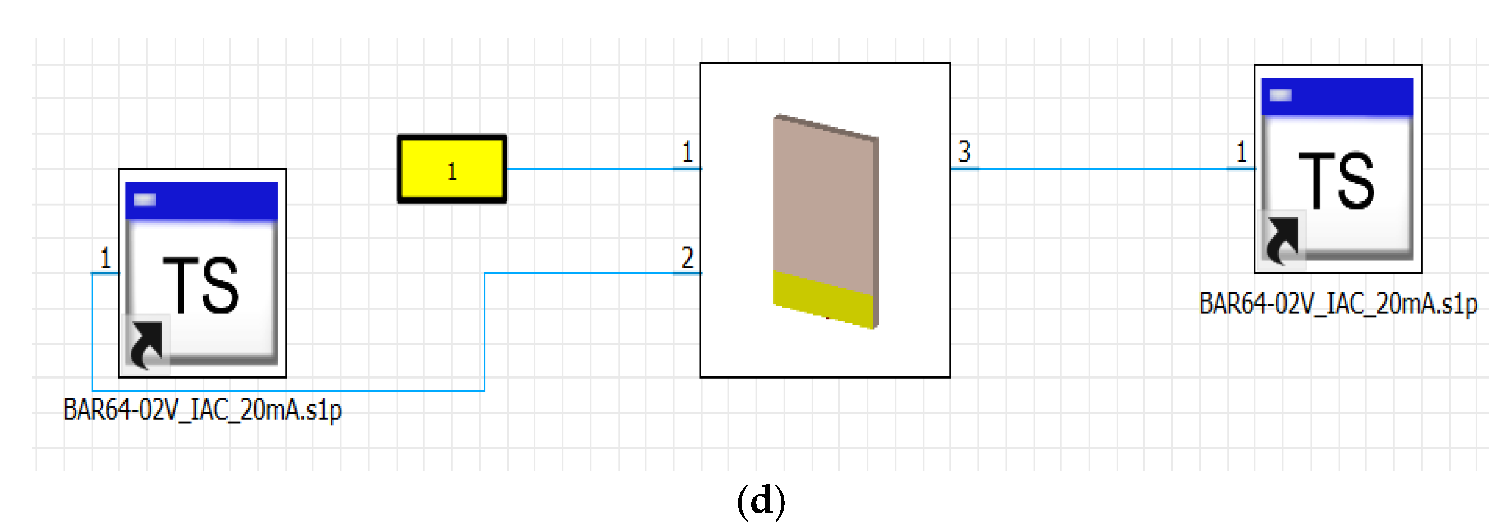
Due to the high demand for the advanced wireless systems, new antenna designs play a crucial role in operating multiple frequency bands. During the design process, it is important that the innovative antenna structures in compact size have to fit into a single wireless device. Hence, this geometric constraint is considered as a main task in this study. A novel antenna geometry is composed of an inner spiral resonator to be connected to the outer split-ring radiator. The main purpose of using resonators and split-ring radiators is to reduce the overall antenna dimension [43,44,45,46,47]. Different side views of the novel proposed antenna structure are detailed in Figure 1a–c. The reconfigurability is accomplished by using two different switching components including PIN diodes, and SPDT switches to alter the electrical length and shape of the radiating element. The dimension of the reconfigurable antenna is calculated by using Equations (1) and (2). The substrate material is FR-4 with relative permittivity of 4.3, loss tangent of 0.025 and thickness of 1.6 mm. The overall dimension of the designed antenna is 22 × 16 × 1.6 mm3. The physical parameters of proposed antenna are labelled in Figure 1a and detailed in Table 1. Two switches are visualized and labelled as D1 and D2 as shown in Figure 1a. CST Studio Suite, a commercial software package for electromagnetic simulations, is used for the analysis of the proposed antenna performance numerically [48]. PIN diodes are modeled by touchstone files including one-port S parameters information as shown in Figure 1d.
The calculation of the width of the feed line (Wf) is initially justified using standard transmission line theory, as referenced in [17,49]. This theory provides a well-established framework for determining the appropriate dimensions of transmission lines, ensuring efficient signal propagation. Additionally, we calculated the effective dielectric constant ( ε e f f ) based on the ratio of the feed line width ( w f ) to the substrate height ( h ) as given in Equation (1) [49]. To match the impedance of 50 Ω, we validated the characteristic impedance ( Z 0 ) of the feed line using Equation (2) [49]. After that, the wavelength (λ) for the lower and upper frequencies was calculated via Equation (3) [17,28,48] to determine the effective resonant lengths (Lon-on and Loff-off) for the antenna states. These lengths were determined as a proportional ratio of λ to achieve the desired resonance. It is important to explain how to calculate the electrical length of for different states. By using Equation (3) the electrical lengths are initially determined as λ 1 = 57   m m and λ 2 = 125   m m for the upper and lower frequencies, respectively. After calculating the wavelength, Lon-on and Loff-off of the proposed antenna for each frequency band (5.2, and 2.4 GHz), parametric analysis is utilized to obtain the optimum values for the other labeled dimensions in Figure 1. By providing these explanations and calculations based on transmission line theory, Table 1 offers a comprehensive understanding of the design parameters and the process behind determining them.
ε e f f = ε r + 1 2 + ε r 1 2 1 + 12 w f h 0.5 where   w h > 1
Z 0 = 120 π ε e f f w f h + 1.393 + 2 3 l n w w f h + 1.44
L R = c 0 4 f c   ε e f f

2.2. Parametric Analysis and Equivalent Circuit

2.2.1. Parametric Analysis

Several critical design parameters are considered when developing the proposed antenna structure, including the dielectric constant, effective dielectric constant, wavelength, and characteristic impedance. To address potential issues, parametric analysis and theoretical calculations are performed. The effective dielectric constants are determined using equations from Bahl and Trivedi’s study [50], which depend on the dielectric height and transmission line width. These equations demonstrate the importance of the effective dielectric constant, dielectric height, and transmission line width for the design. By using the above Equations (1)–(3), initial fundamental physical parameters are calculated to define the operating frequency ranges for different states of the antenna. Then, the geometrical parameters labeled in Figure 1a are studied through calculations and parametric analysis. By analyzing the reflection coefficient for each set of parameter values, the antenna’s performances are assessed and compared. The goal is to find the combination of parameters that achieves the optimal antenna performance with the optimized values in Table 1.

2.2.2. Equivalent Circuit Model

The impedance mismatch issue is a common challenge when using a common feed line for a reconfigurable antenna. To address this problem, an equivalent circuit model is often employed. This model offers a valuable approach for resolving the impedance mismatch by introducing a lumped element for different parts of the antenna. To determine the correct value for the lumped element, it is crucial to accurately model the antenna. In this study, detailed equivalent circuits are utilized for ON-ON and OFF-OFF states in Figure 2. Each circuit elements are calculated separately for the corresponding resonance based on Equation (4). By using Equation (4), each value is calculated and inserted into the equivalent circuit of the proposed antenna given in Figure 2.
f r = 1 2 π L C
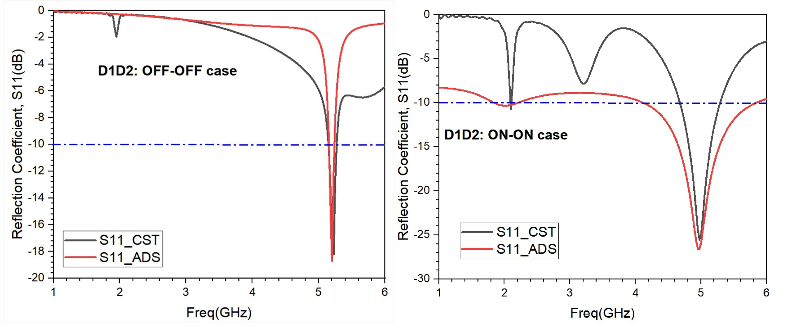
Based on the provided equivalent circuit models, Figure 3 outlines that the reflection coefficient of the antenna design has been analyzed and compared using two different software tools: CST and Advanced Design System (ADS). By comparing the reflection coefficients obtained from these two software tools, the performance of the antenna design is validated through equivalent circuit models of ON-ON and OFF-OFF states.

2.3. Fabricated Designs

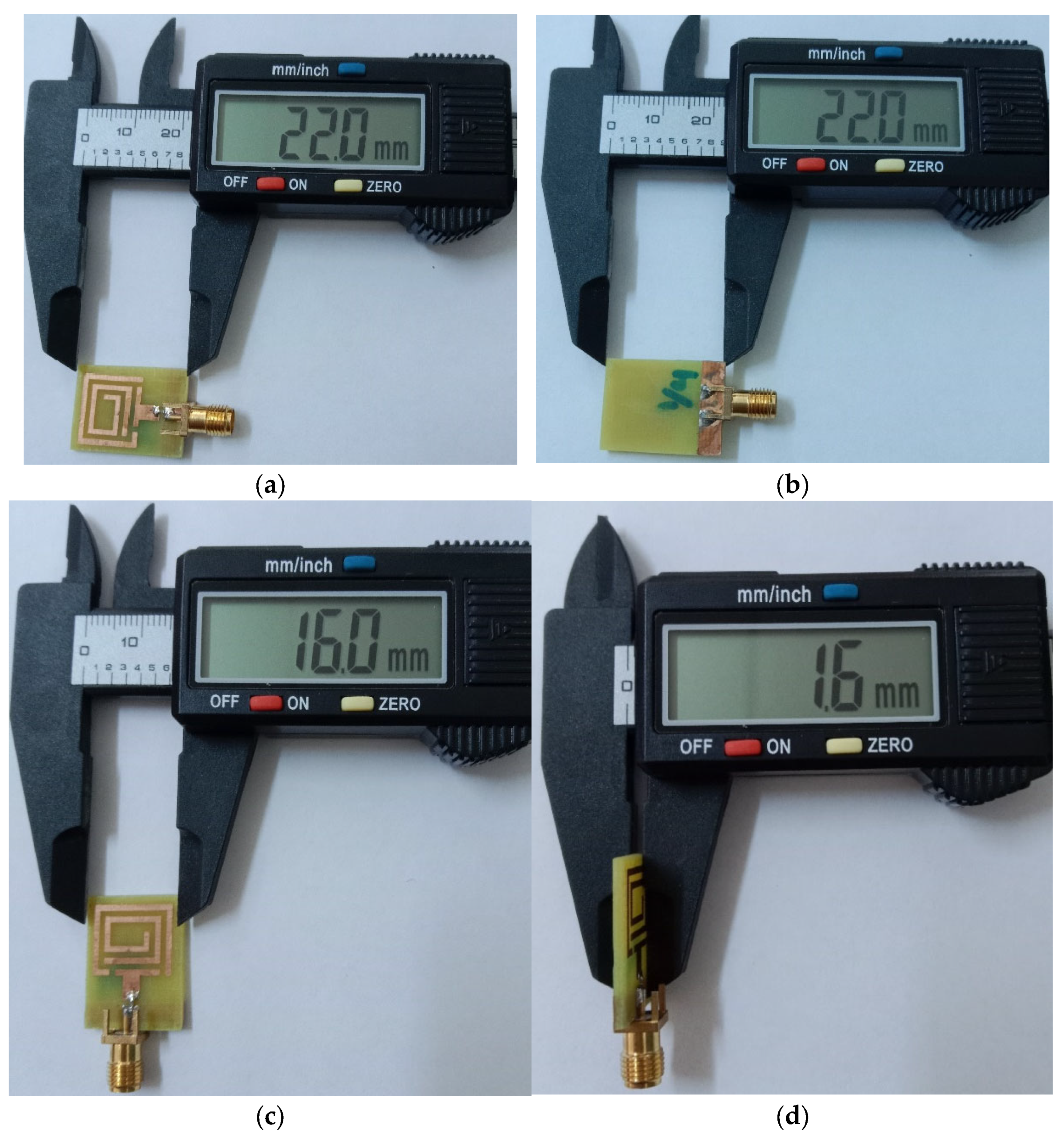
The feasibility and effectiveness of the proposed antenna design are validated by fabricating antenna prototypes on FR-4 substrate using the design parameters and geometries obtained from numerical analysis. The dimensions and physical parameters are determined through numerical analysis. The main goal of this process is to ensure that the antenna performs as intended and meets the compact size requirements for integration into wireless devices. The chemical etching methods are utilized to fabricate the biasing circuitry, and two proposed antenna structures owing to the pros including versatility and cost-effectiveness techniques. First, the antenna profile is presented from the back, front, and side views using digital meter measurements in Figure 4a–d, respectively. These visual representations given in Figure 4a–d offer a clear and accurate depiction of the antenna’s physical dimensions, shape, and structural characteristics. It is deduced from this analysis that the proposed antenna design has a low-profile structure.
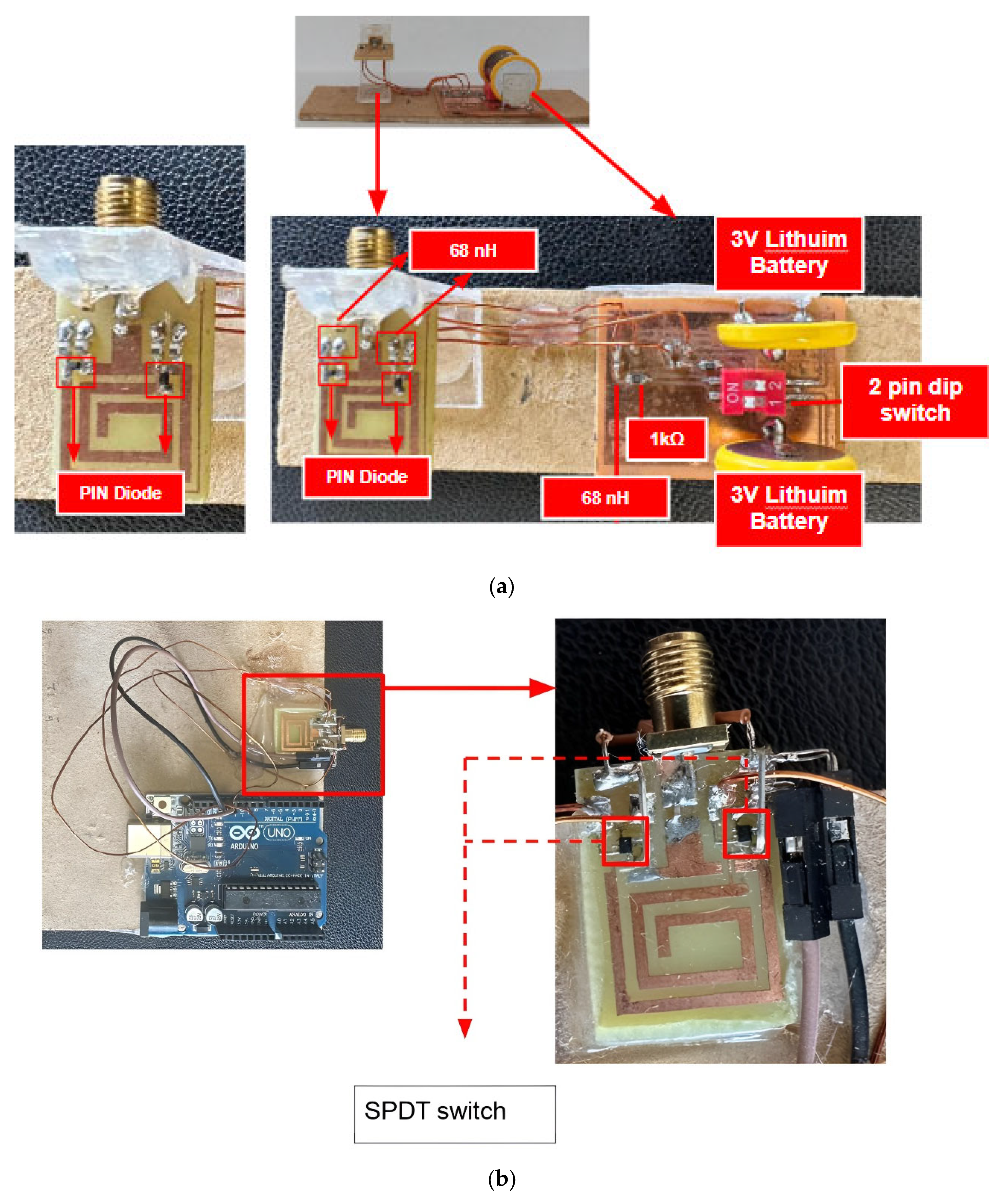
In Figure 5a, the implementation of the proposed antenna structure involves soldering two BAR64−02V PIN diodes and a DC Block Capacitor of 100 pF into the corresponding gaps of the antenna. The PIN diodes serve as the switching components responsible for the reconfigurability of the antenna, allowing the control of its operating states. The DC Block Capacitor is used to separate the DC and RF signals, preventing interference and enabling accurate comparison between the numerically calculated and measured results. Figure 3a also shows the implementation of the biasing circuitry, which is an integral part of the antenna design. The biasing network consists of two CR2032—3 pin vertical 3 V lithium batteries, 2 PIN dip switch, 68 nH inductor, and a 1 kΩ resistor. Figure 5b depicts the proposed antenna with an RF switch controlled by Arduino. DC block capacitor with a value of 100 pF, is also utilized for this design as represented in Figure 5b.
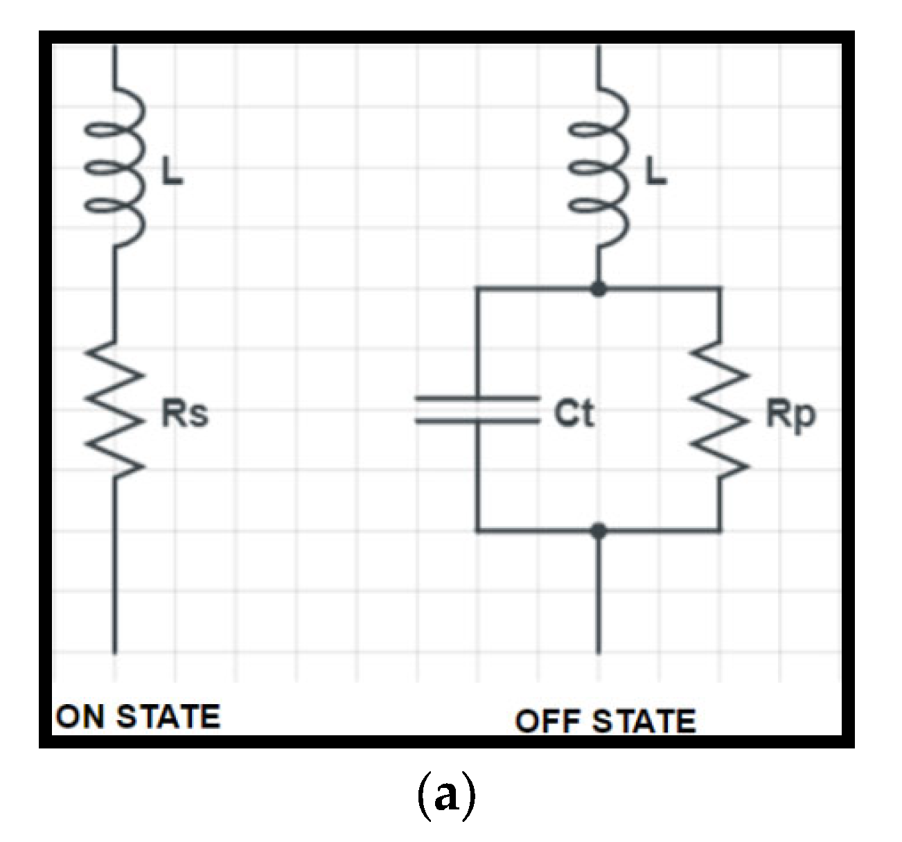
Knowing the equivalent circuit behavior of the PIN diode BAR64−02V plays a paramount role in designing and fabricating the frequency reconfigurable antennas. It also helps to optimize the antenna’s performance, analyze its reconfigurability, predict its behavior, and guide the fabrication process, ultimately leading to the development of efficient and reliable frequency reconfigurable antenna systems. Hence, Figure 6a illustrates the equivalent circuit model of the BAR64−02V PIN diode. It is also clear from the equivalent circuit of the PIN diodes that when a PIN diode is forward-biased (positive voltage applied to the P-region and negative voltage applied to the N-region), it behaves as a series combination of low-resistance and inductor, allowing current to flow through it. This forward-biased condition is referred to as the ON state of the PIN diode. Conversely, when a PIN diode is reverse-biased (positive voltage applied to the N-region and negative voltage applied to the P-region), it exhibits a parallel combination of high resistance and capacitor and series with the inductor. This reverse-biased condition is referred to as the OFF state of the PIN diode.
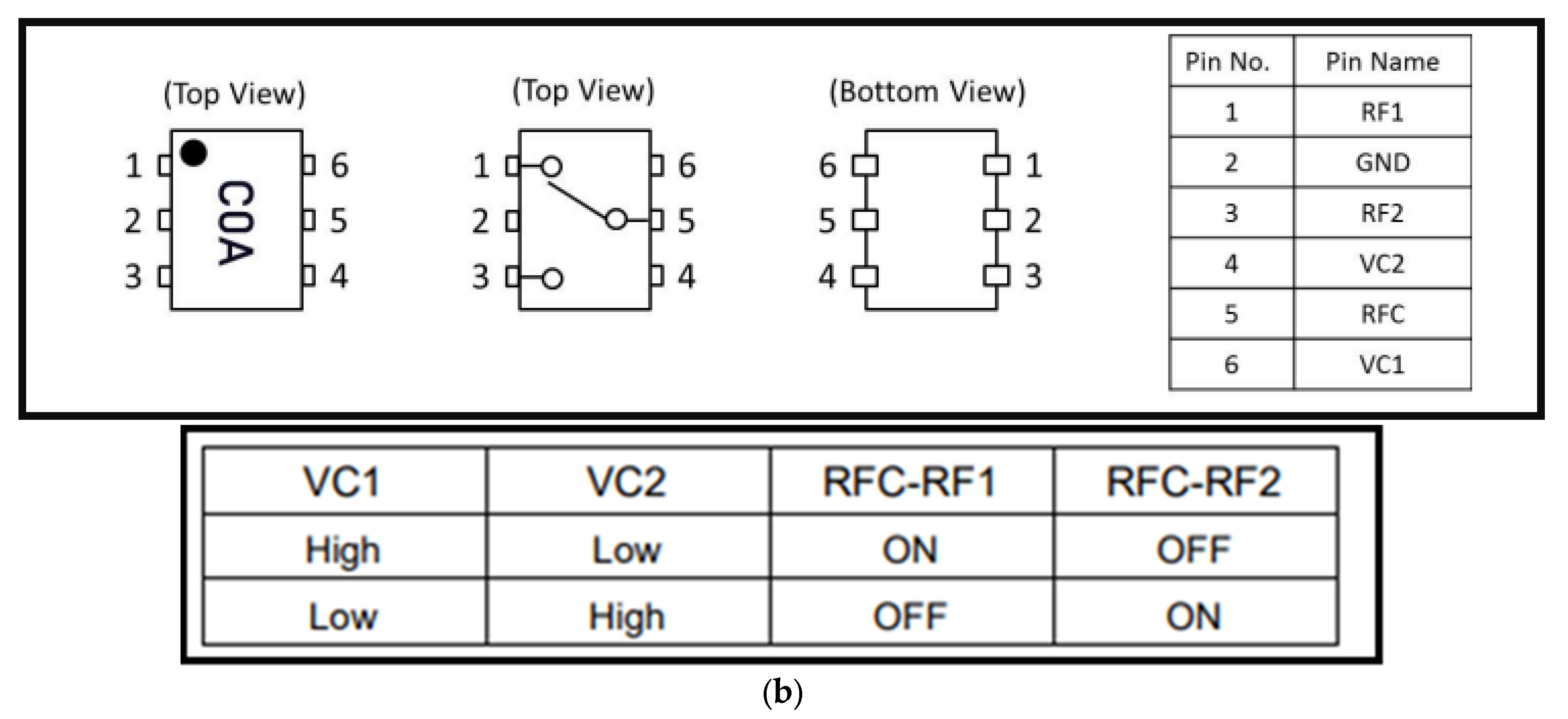
On the other hand, knowing the block diagram and evaluation circuit of SPDT switches, such as the CG2415M6, provides designers to understand the functionality, control mechanisms, and performance characteristics of the switch. It also aids in the design, integration, and fabrication of frequency reconfigurable antennas by ensuring proper signal routing, control, power handling, and performance evaluation. Based on these restrictions, the truth table and block diagram of SPDT switches, whose models are CG2415M6, are represented in Figure 6b [51]. SPDT switch is a type of electrical switch that consists of a single input or common terminal (COM) and two output terminals known as the normally open (NO) and normally closed (NC) terminals as shown in the top view. The working principle of an SPDT switch involves the actuation of a mechanical mechanism to change the connection between these terminals. In its resting or unactuated position, the COM terminal (pin 5) is electrically connected to the NC terminal (pin 1), whereas the NO terminal (pin 3) is disconnected. This means that when the switch is not pressed or flipped, the circuit is completed between the COM and NC terminals, allowing current to flow through that path. When the switch is actuated or flipped, the mechanical mechanism inside the switch moves, causing the connection to change. In this new position, the COM terminal becomes connected to the NO terminal, and the connection between COM and NC is broken. This means that when the switch is pressed or flipped, the circuit is completed between the COM and NO terminals instead, redirecting the current flow through that path. The SPDT switch is commonly used to select between two different circuits or to switch between two different paths within a circuit. The COM terminal is typically connected to the input or source, whereas the NO and NC terminals are connected to different outputs or destinations. By actuating the switch, the connection can be changed from one output to another. In this study, the COM (Common) terminal of the SPDT switch is connected to one of the digital input pins (e.g., pin 2) on the Arduino Uno. The NO (Normally Open) terminal of the switch is connected to the Arduino’s 3 V power supply. The NC (Normally Closed) terminal of the switch is connected to the ground (GND) on the Arduino. It is also crucial to take into consideration that the remaining terminal (NO or NC, depending on the one that is used in the previous step) should be connected to the GND (ground) pin on the Arduino Uno. After the connection of the terminals to the Arduino Uno, the coding is determined based on the connections. In other words, based on the switch state, the appropriate code is written to perform specific actions, control other components, or make decisions in your Arduino program.

3. Results and Discussions

3.1. Simulation Results

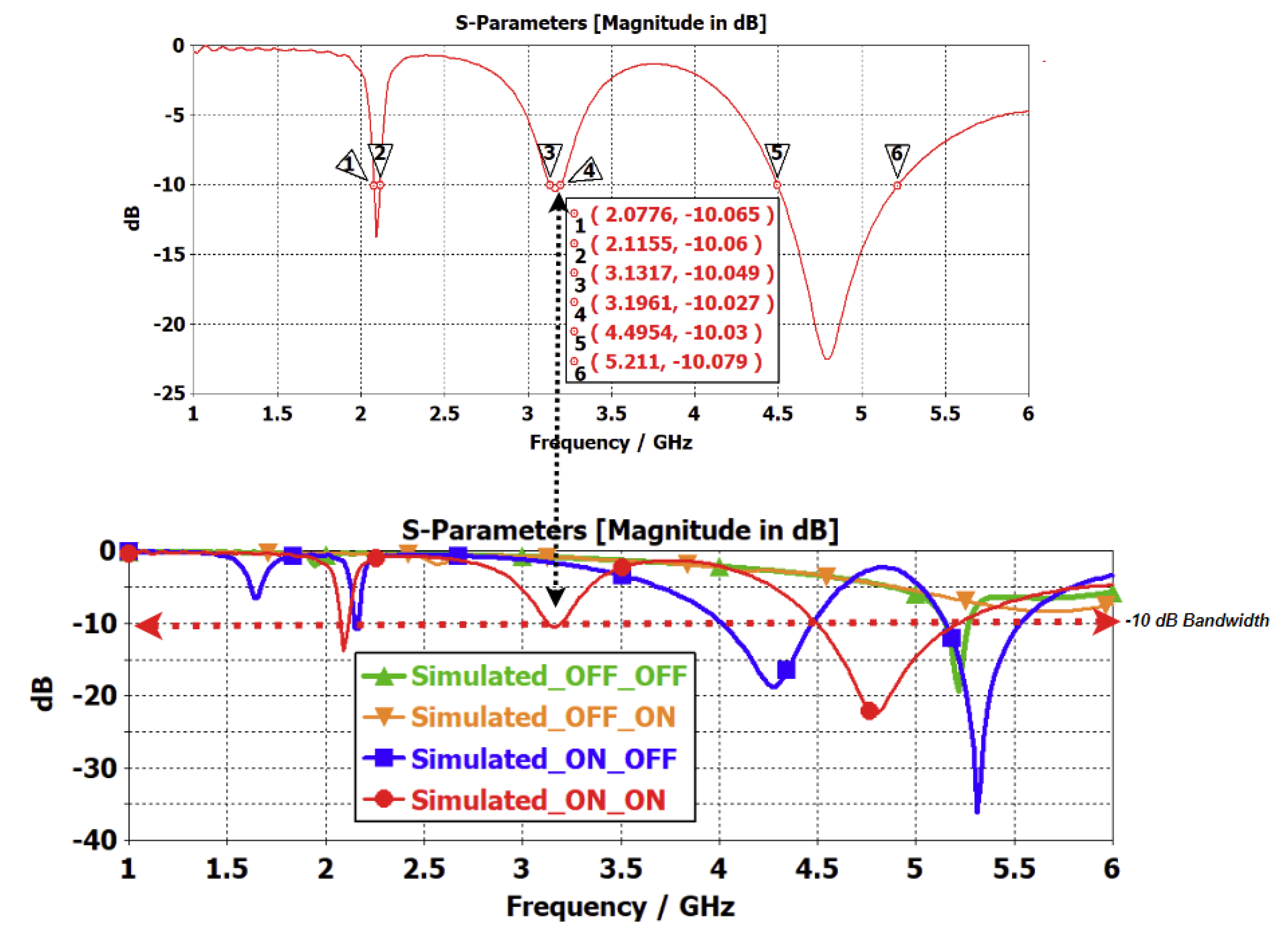
The proposed antenna structure is simulated with four different configurations to analyze the impact of switch states on operating frequencies and resonance frequencies. The simulation results, presented in Figure 7, show the reflection coefficients of the antenna with and without switches. The figure demonstrates that changing the switch states significantly affects the frequencies at which the antenna operates and resonates.
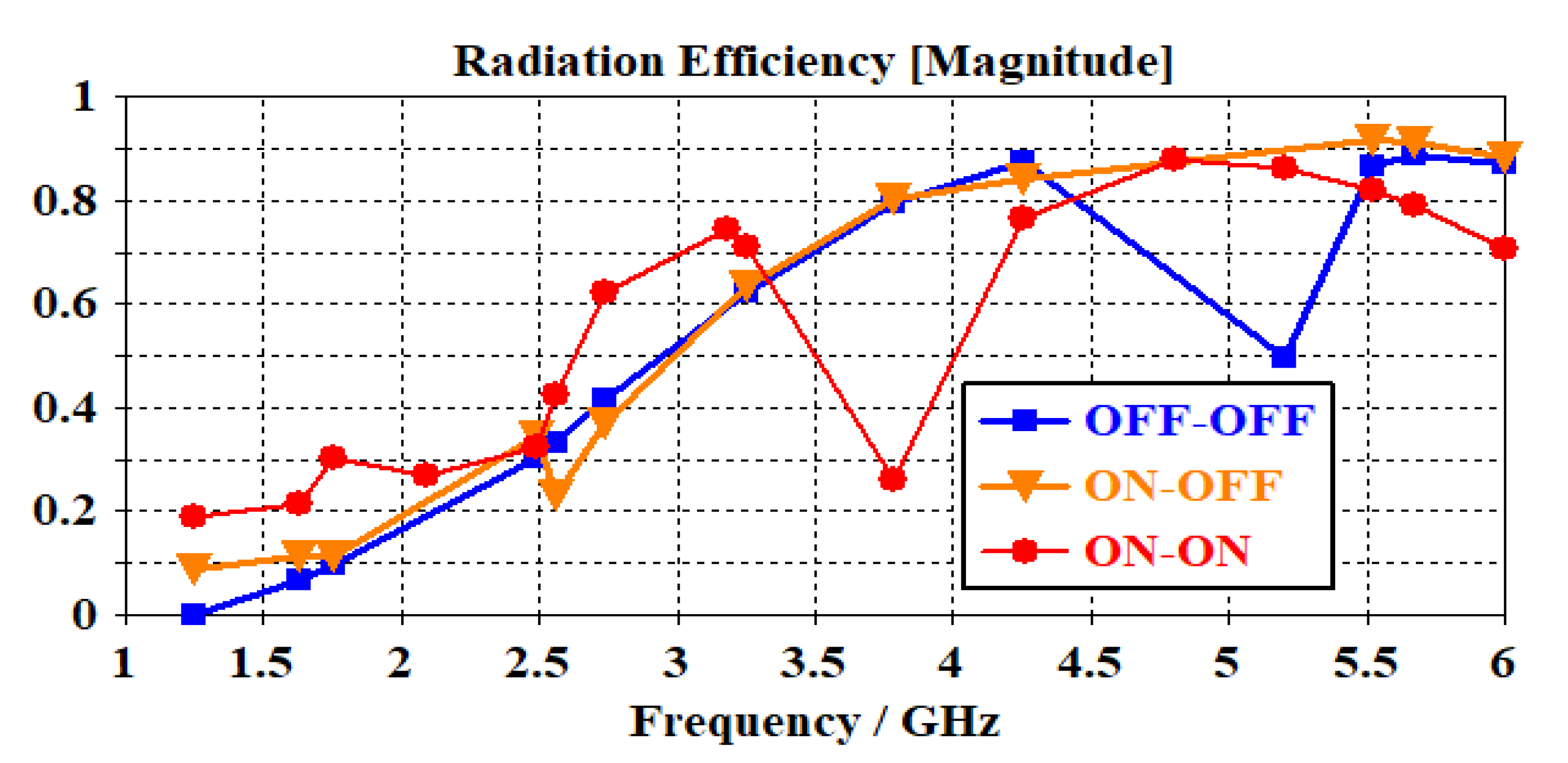
Figure 8 illustrates the radiation efficiency parameter of the proposed antenna in different configurations. Radiation efficiency is a crucial metric that indicates system performance, signal strength range, and power efficiency. The results indicate that the proposed antenna, with its compact size, is well-suited for sub-6 GHz applications. This suggests the designed antenna is a strong candidate for such applications. The radiation efficiency of the OFF-ON state is not explicitly provided in Figure 8 due to the influence of spiral resonators on the antenna’s non-radiation characteristics, particularly in applications below 6 GHz. The focus of Figure 6 is to illustrate other pertinent states related to the antenna’s performance, such as reflection coefficient and bandwidth.
Table 2 provides an overview of the antenna’s performance parameters and their corresponding application areas for all configurations. The table further supports the notion that the proposed design holds great promise for sub-6 GHz applications. Its performance metrics highlight its suitability for a wide range of applications within this frequency range.
By presenting these simulation results and performance parameters, it becomes evident that the proposed antenna design, with its versatility and compact size, offers significant potential for sub-6 GHz applications. These findings strengthen the case for its inclusion in relevant research and development efforts.
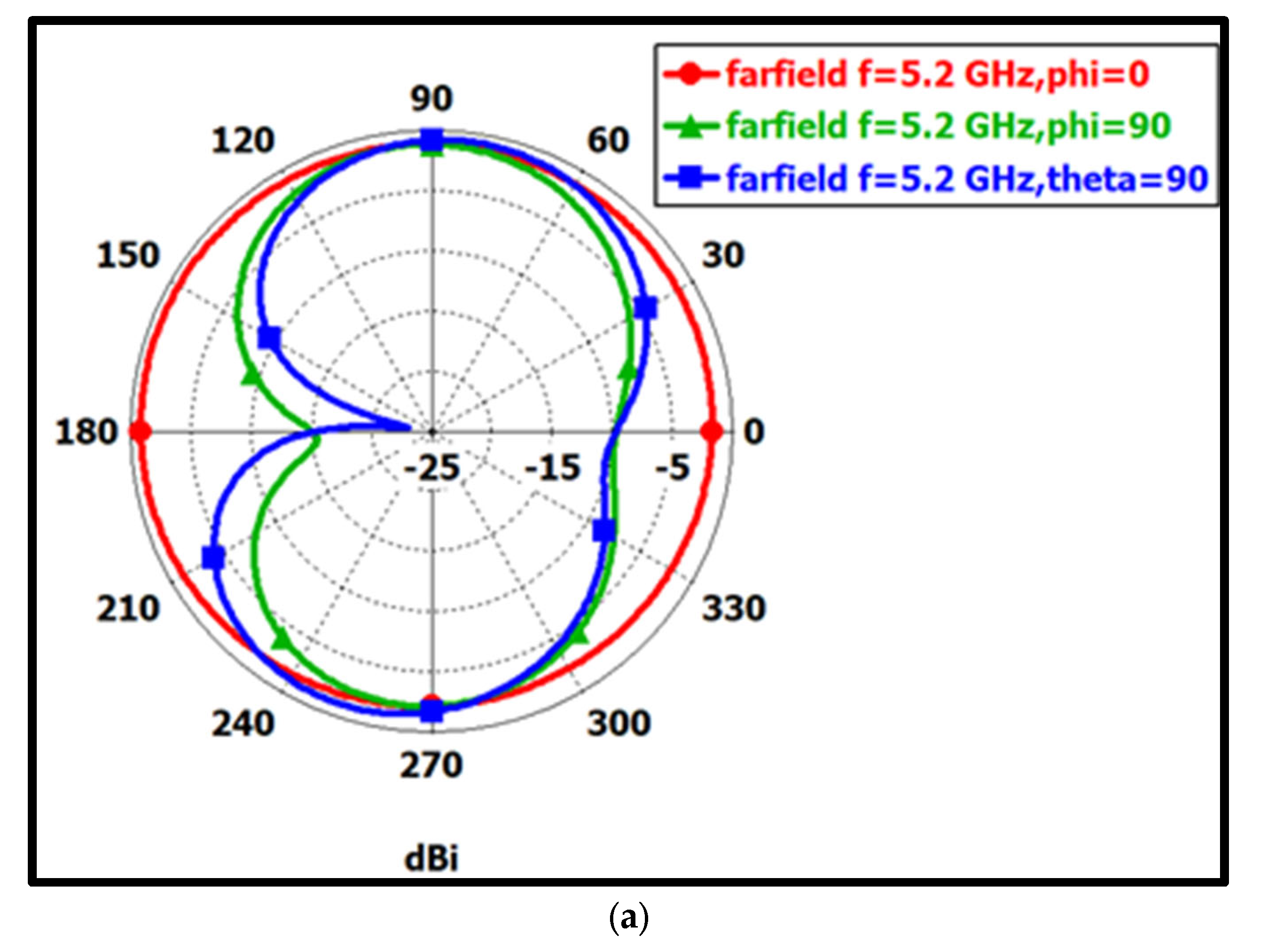
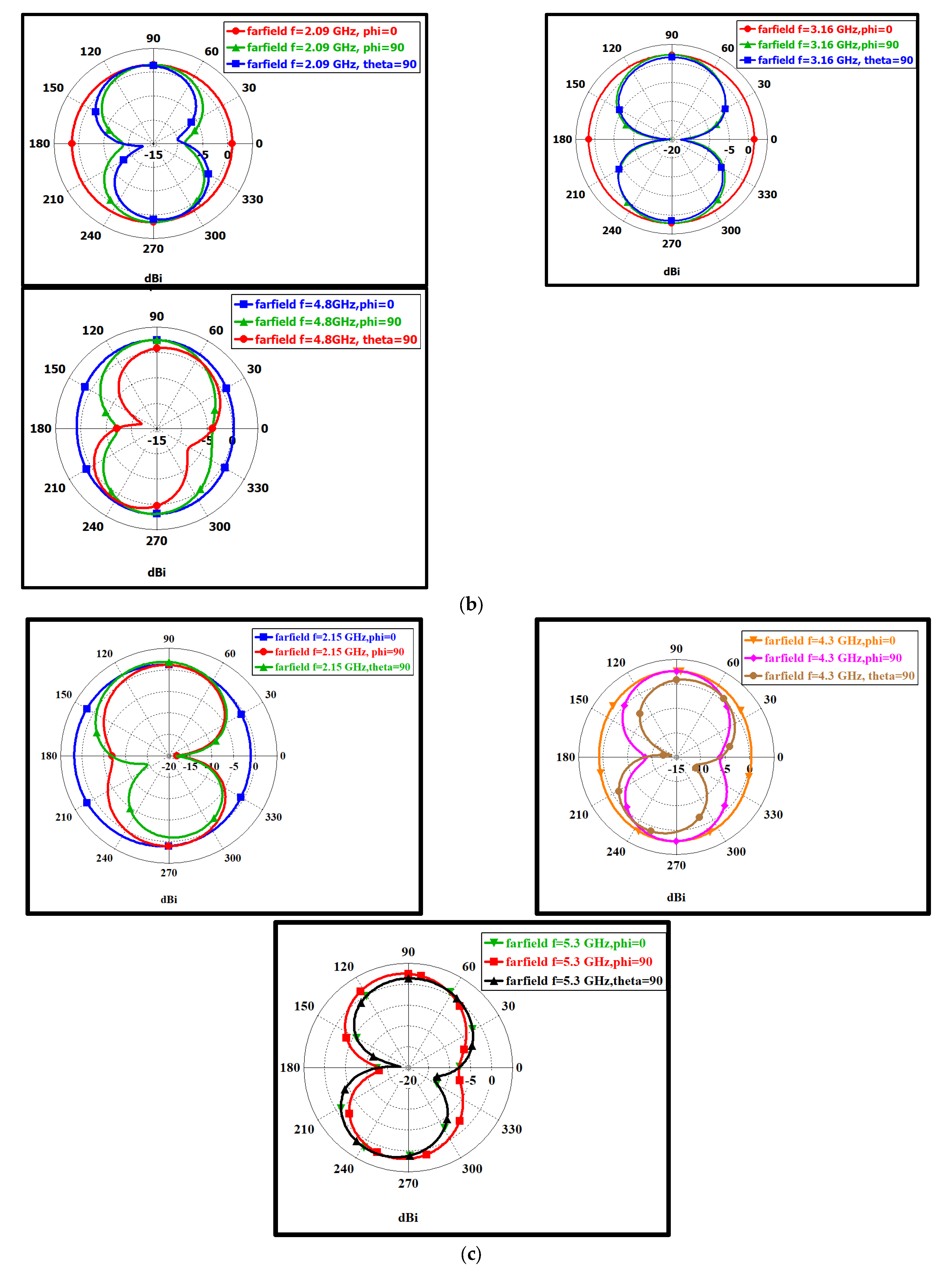
Figure 9 depicts the radiation patterns at the resonance frequencies for three conditions. It is clear from Figure 9 that all radiation patterns have almost omnidirectional patterns in the frequency range of interest. It is also worth mentioning that omnidirectional radiation pattern yields better performance for wireless communication systems to access devices from any direction.

3.2. Measurement Results

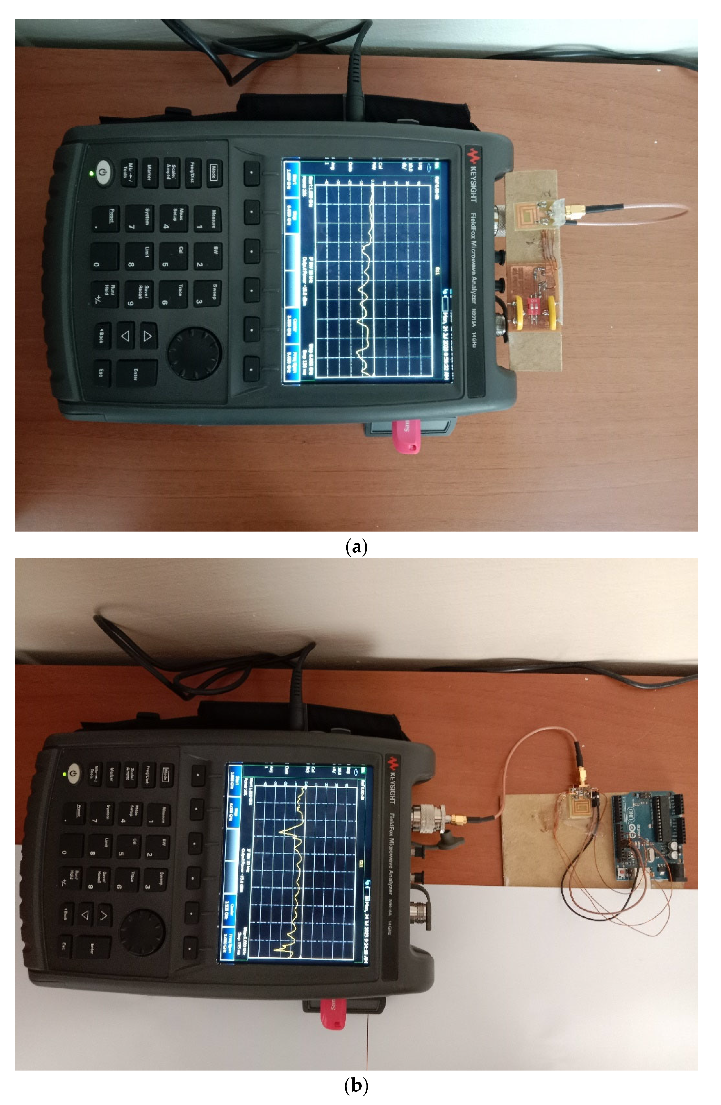
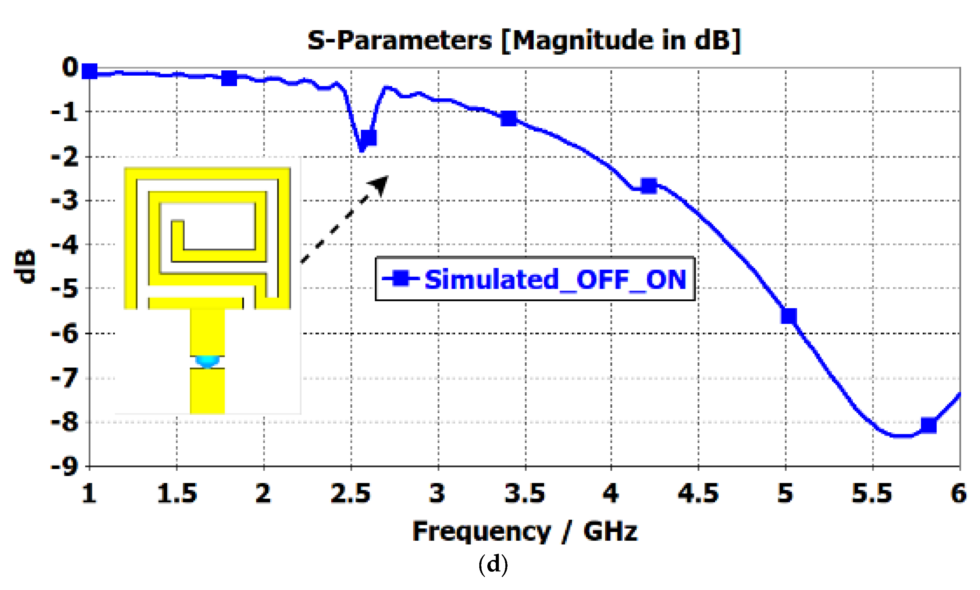
The experimental setups are utilized for the proposed antenna with PIN diodes and SPDT switches as given in Figure 10. The main goal of the experimental process is to ensure that the physical realization of the antenna aligns with the intended design specifications. The measurement results of the fabricated antenna for different states are obtained in terms of reflection coefficients in Figure 11a–d to compare the numerically calculated and measured results. Figure 11a outlines the measured and simulated reflection coefficient of the OFF-OFF configuration. As seen in Figure 11a, the resonance frequency is almost identical for the simulation and measurement results. It is also clear from Figure 11a that there is a discrepancy between the simulated and measured reflection coefficient of the proposed antenna with PIN diodes. As seen from the ON-ON state given in Figure 11b, the simulation and measurement results of the proposed antenna with SPDT switches are in good agreement whereas the measurement results with PIN diodes are not compatible with the simulation result. Then, Figure 11c illustrates the comparison of the simulation and measurement results for the proposed antenna with an ON-OFF configuration. It is deduced from Figure 11c that the simulation result is compatible with the measurement result of the proposed antenna with the SPDT switch. Figure 11d depicts that the proposed antenna configuration does not radiate in the sub-6 GHz frequency range due to the effect of the spiral resonator because the spiral resonator introduces impedance variations at its resonant frequencies. This restriction causes an impedance mismatch between the spiral resonator and the feeding network. On the other hand, the addition of the spiral resonator results in additional resonator modes, which originate the undesired frequency shifts and distortions.
The measurement results of the proposed antenna with PIN diodes and SPDT switches can differ from each other due to several factors. First of all, PIN diodes and SPDT switches have different characteristics and switching mechanisms. PIN diodes typically have a slower switching speed compared to solid-state switches like SPDT switches. This difference in switching speed can affect the antenna’s performance, especially in dynamic or fast-changing scenarios. SPDT switches are used to provide faster and more reliable switching, resulting in better overall antenna performance. Secondly, the insertion loss of the switching components varies between PIN diodes and SPDT switches. Insertion loss refers to the loss of signal power when it passes through the switching element. PIN diodes may introduce higher insertion loss compared to SPDT switches, which can impact the antenna’s overall efficiency and gain. PIN diodes and SPDT switches also have different RF impedance characteristics. These impedance differences affect the matching network and impedance matching of the antenna. That is why the impedance is not properly matched; it leads to signal reflections, reduced power transfer, and degraded antenna performance. The control circuitry for PIN diodes and SPDT switches may differ in terms of complexity, biasing, and control voltages. If the control circuitry is not properly designed or implemented, the measured result introduces additional losses or mismatches, impacting the antenna’s performance differently for PIN diodes and SPDT switches. Each switching component introduces parasitic effects that can affect the antenna’s behavior. These parasitic effects include capacitance, inductance, and resistance associated with the switches themselves or their control circuitry. The parasitic effects can vary between PIN diodes and SPDT switches, leading to different impacts on the antenna performance. On the other hand, variations occur due to the chemical etching process since manufacturing variations can lead to slight differences in the antenna dimensions and affect its performance parameters such as resonant frequency, and impedance.
Table 3 outlines the comparison of the proposed novel antenna structure with the other frequency reconfigurable antennas in the literature. It is clear from Table 3 that the proposed antenna outperforms the other frequency reconfigurable antennas in the literature in terms of compactness, wide operating frequency range, and low cost. Furthermore, the control method of the used components, which provide reconfigurability features, is also compared. The proposed novel antenna can be integrated into many devices including access points, gateways, smartphones, and IoT kits due to its tiny size and easy control mechanism.

4. Conclusions

In this study, a novel frequency reconfigurable antenna design for sub-6 GHz applications is proposed, featuring a unique combination of antenna elements and control mechanisms. The antenna consists of an outer split-ring resonator loaded with an inner spiral resonator, and its reconfigurability is achieved through the remote control of the PIN diode or SPDT switches. Experimental measurements and numerical computations validate the antenna’s performance, highlighting its superiority over existing alternatives in terms of compactness, wide operating frequency range, and cost-effectiveness. Compared to the existing literature, the proposed antenna design offers several significant advancements. Firstly, the antenna operates in broadband or tri-band mode, allowing for versatile applications. The utilization of PIN diodes or SPDT switches as RF switches provide efficient frequency reconfigurability. Furthermore, the omnidirectional radiation pattern of the antenna enhances its suitability for wireless communication systems. The experimental results demonstrate the antenna’s effectiveness on an FR-4 substrate, confirming its performance and validating the numerical calculations. The antenna’s compact size and easy control mechanism make it highly suitable for integration into various devices such as access points, gateways, smartphones, and IoT kits. In terms of application potential, the proposed design shows promise in a wide range of areas, including Wi-Fi (IEEE 802.11 a/n/ac), Bluetooth (5 GHz), ISM (5 GHz), 3G (UMTS), 4G (LTE), wireless backhaul (4G and 5G networks), WLAN (IEEE 802.11a/n/ac/ax), and 5G NR n1 band. Its versatility and compatibility with different wireless communication standards open up new opportunities for deployment in various scenarios. This novel frequency reconfigurable antenna design makes a valuable contribution to the field, surpassing existing literature in terms of its unique combination of antenna elements, control mechanisms, performance advantages, and application potential. The findings of this study lay the foundation for further advancements in wireless communication systems and inspire future research and development efforts in the field of frequency reconfigurable antennas.

Author Contributions

Conceptualization, D.N.G., Ş.Ç. and M.P.; Methodology, D.N.G., Ş.Ç. and M.P.; Software, D.N.G.; Validation, D.N.G., Ş.Ç. and M.P.; Formal analysis, D.N.G. and M.P.; Investigation, D.N.G., Ş.Ç. and M.P.; Writing—original draft, D.N.G.; Writing—review & editing, D.N.G., Ş.Ç. and M.P.; Supervision, Ş.Ç. and M.P. All authors have read and agreed to the published version of the manuscript.

Funding

This research received no external funding.

Data Availability Statement

Not applicable.

Acknowledgments

This work is supported by the Scientific Research Projects Unit (BAP) in Adana Alparslan Türkeş Science and Technology University. Project No: 21803003.

Conflicts of Interest

The authors declare no conflict of interest.

References

  1. Yusifov, S.I.; Ragimova, N.A.; Abdullayev, V.H.; Imanova, Z.B. 5G Technology: A New Step to IoT Platform. JINAV J. Inf. Vis. 2020, 1, 74–82. [Google Scholar] [CrossRef]
  2. West, D.M. How 5G technology enables the health internet of things. Brook. Cent. Technol. Innov. 2016, 3, 20. [Google Scholar]
  3. Li, S.; Da Xu, L.; Zhao, S. 5G Internet of Things: A survey. J. Ind. Inf. Integr. 2018, 10, 1–9. [Google Scholar] [CrossRef]
  4. Andrews, J.G.; Buzzi, S.; Choi, W.; Hanly, S.V.; Lozano, A.; Soong, A.C.; Zhang, J.C. What will 5G be? IEEE J. Sel. Areas Commun. 2014, 32, 1065–1082. [Google Scholar] [CrossRef]
  5. Goudos, S.K.; Dallas, P.I.; Chatziefthymiou, S.; Kyriazakos, S. A survey of IoT key enabling and future technologies: 5G, mobile IoT, sematic web and applications. Wirel. Pers. Commun. 2017, 97, 1645–1675. [Google Scholar] [CrossRef]
  6. Güneş, F.; Evranos, İ.Ö.; Belen, M.A.; Mahouti, P.; Palandöken, M. A compact triband antipodal vivaldi antenna with frequency selective surface inspired director for IoT/WLAN applications. Wirel. Netw. 2021, 27, 3195–3205. [Google Scholar] [CrossRef]
  7. Mohammed, A.S.; Kamal, S.; Ain, M.F.B.; Hussin, R.; Najmi, F.; Sundi, S.A.; Othman, M. Mathematical model on the effects of conductor thickness on the centre frequency at 28 GHz for the performance of microstrip patch antenna using air substrate for 5G application. Alex. Eng. J. 2021, 60, 5265–5273. [Google Scholar] [CrossRef]
  8. Iqbal, J.; Illahi, U.; Yasin, M.N.M.; Albreem, M.A.; Akbar, M.F. Bandwidth enhancement by using parasitic patch on dielectric resonator antenna for sub-6 GHz 5G NR bands application. Alex. Eng. J. 2022, 61, 5021–5032. [Google Scholar] [CrossRef]
  9. Shereen, M.K.; Khattak, M.I.; Nebhen, J. A review of achieving frequency reconfiguration through switching in microstrip patch antennas for future 5G applications. Alex. Eng. J. 2022, 61, 29–40. [Google Scholar] [CrossRef]
  10. Kamal, S.; Ain, M.F.B.; Ullah, U.; Mohammed, A.S.; Najmi, F.; Hussin, R.; Othman, M. Wheel-shaped miniature assembly of circularly polarized wideband microstrip antenna for 5G mmWave terminals. Alex. Eng. J. 2021, 60, 2457–2470. [Google Scholar] [CrossRef]
  11. Kumar, S.A.; Shanmuganantham, T.; Dileepan, D. Design and development of CPW fed monopole antenna at 2.45 GHz and 5.5 GHz for wireless applications. Alex. Eng. J. 2017, 56, 231–234. [Google Scholar] [CrossRef]
  12. Nashaat, D.M.; Elsadek, H.A.; Ghali, H. Single feed compact quad-band PIFA antenna for wireless communication applications. IEEE Trans. Antennas Propag. 2005, 53, 2631–2635. [Google Scholar] [CrossRef]
  13. Karli, R.; Ammor, H. A simple and original design of multi-band microstrip patch antenna for wireless communication. Int. J. Microw. Appl. 2013, 2, 41–44. [Google Scholar]
  14. Zhu, X.Q.; Guo, Y.X.; Wu, W. A novel dual-band antenna for wireless communication applications. IEEE Antennas Wirel. Propag. Lett. 2015, 15, 516–519. [Google Scholar] [CrossRef]
  15. Sun, L.; He, M.; Hu, J.; Zhu, Y.; Chen, H. A butterfly-shaped wideband microstrip patch antenna for wireless communication. Int. J. Antennas Propag. 2015, 2015, 328208. [Google Scholar] [CrossRef] [Green Version]
  16. Schaubert, D.H.; Farrar, F.G.; Hayes, S.T.; Sindoris, A.R.; Department Of the Army Washington DC. Frequency-Agile, Polarization Diverse Microstrip Antennas and Frequency Scanned Arrays. U.S. Patent 4367474, 1 April 1983. [Google Scholar]
  17. Ullah, S.; Ahmad, S.; Khan, B.A.; Tahir, F.A.; Flint, J.A. An hp-shape hexa-band antenna for multi-standard wireless communication systems. Wirel. Netw. 2019, 25, 1361–1369. [Google Scholar] [CrossRef]
  18. Vamseekrishna, A.; Madhav, B.T.P.; Anilkumar, T.; Reddy, L.S.S. An IoT controlled octahedron frequency reconfigurable multiband antenna for microwave sensing applications. IEEE Sens. Lett. 2019, 3, 3502204. [Google Scholar] [CrossRef]
  19. Zhao, X.; Riaz, S. A dual-band frequency reconfigurable MIMO patch-slot antenna based on reconfigurable microstrip feedline. IEEE Access 2018, 6, 41450–41457. [Google Scholar] [CrossRef]
  20. Han, L.; Wang, C.; Chen, X.; Zhang, W. Compact frequency-reconfigurable slot antenna for wireless applications. IEEE Antennas Wirel. Propag. Lett. 2016, 15, 1795–1798. [Google Scholar] [CrossRef]
  21. Arun, V.; Marx, L.K. Internet of Things controlled reconfigurable antenna for RF harvesting. Def. Sci. J. 2018, 68, 566–571. [Google Scholar]
  22. Zaidi, A.; Awan, W.A.; Hussain, N.; Baghdad, A. A Wide and Tri-band Flexible Antennas with Independently Controllable Notch Bands for Sub-6-GHz Communication System. Radioengineering 2020, 29, 44–51. [Google Scholar] [CrossRef]
  23. Cai, Y.M.; Li, K.; Yin, Y.; Gao, S.; Hu, W.; Zhao, L. A low-profile frequency reconfigurable grid-slotted patch antenna. IEEE Access 2018, 6, 36305–36312. [Google Scholar] [CrossRef]
  24. Allam, V.K.; Madhav, B.T.; Anilkumar, T.; Maloji, S. A novel reconfigurable bandpass filtering antenna for IoT communication applications. Prog. Electromagn. Res. C 2019, 96, 13–26. [Google Scholar] [CrossRef] [Green Version]
  25. Soltanpour, M.; Fakharian, M.M. Compact filtering slot antenna with frequency agility for Wi-Fi/LTE mobile applications. Electron. Lett. 2016, 52, 491–492. [Google Scholar] [CrossRef]
  26. Abdulraheem, Y.I.; Oguntala, G.A.; Abdullah, A.S.; Mohammed, H.J.; Ali, R.A.; Abd-Alhameed, R.A.; Noras, J.M. Design of frequency reconfigurable multiband compact antenna using two PIN diodes for WLAN/WiMAX applications. IET Microw. Antennas Propag. 2017, 11, 1098–1105. [Google Scholar] [CrossRef] [Green Version]
  27. Ali, T.; Khaleeq, M.M.; Biradar, R.C. A multiband reconfigurable slot antenna for wireless applications. AEU-International J. Electron. Commun. 2018, 84, 273–280. [Google Scholar] [CrossRef]
  28. Ghaffar, A.; Li, X.J.; Awan, W.A.; Iffat Naqvi, S.; Hussain, N.; Seet, B.C.; Limiti, E. Design and realization of a frequency reconfigurable multimode antenna for ISM, 5G-sub-6-GHz, and S-band applications. Appl. Sci. 2021, 11, 1635. [Google Scholar] [CrossRef]
  29. Koc Polat, H.; Geyikoglu, M.D.; Cavusoglu, B. Modeling and validation of a new reconfigurable patch antenna through equivalent lumped circuit-based design for minimum tuning effort. Microw. Opt. Technol. Lett. 2020, 62, 2335–2345. [Google Scholar] [CrossRef]
  30. Shah, I.A.; Hayat, S.; Basir, A.; Zada, M.; Shah, S.A.A.; Ullah, S. Design and analysis of a hexa-band frequency reconfigurable antenna for wireless communication. AEU-Int. J. Electron. Commun. 2019, 98, 80–88. [Google Scholar] [CrossRef]
  31. Suzdalenko, A.; Chub, A. Current sensorless control for half-bridge-based AC/DC PFC converter with consideration of conduction losses. Int. J. Circuit Theory Appl. 2016, 44, 2072–2084. [Google Scholar] [CrossRef]
  32. Zhang, S.; Huff, G.H.; Feng, J.; Bernhard, J.T. A pattern reconfigurable microstrip parasitic array. IEEE Trans. Antennas Propag. 2004, 52, 2773–2776. [Google Scholar] [CrossRef]
  33. Trinh, L.H.; Le, T.N.; Staraj, R.; Ferrero, F.; Lizzi, L. A pattern-reconfigurable slot antenna for IoT network concentrators. Electronics 2017, 6, 105. [Google Scholar] [CrossRef] [Green Version]
  34. Costantine, J.; Kanj, R.; Ghorayeb, Z.; Al Bahar, T.; Itani, Y.; Tawk, Y.; Christodoulou, C.G. A radiation pattern reconfigurable antenna for WLAN access. In Proceedings of the 2016 United States National Committee of URSI National Radio Science Meeting (USNC-URSI NRSM), Boulder, CO, USA, 6–9 January 2016; pp. 1–2. [Google Scholar]
  35. Cheung, S.W.; Zhou, C.F.; Li, Q.L.; Yuk, T.I. A simple polarization-reconfigurable antenna. In Proceedings of the 2016 10th European Conference on Antennas and Propagation (EuCAP), Davos, Switzerland, 10–15 April 2016; pp. 1–4. [Google Scholar]
  36. Al-Yasir, Y.I.; Abdullah, A.S.; Ojaroudi Parchin, N.; Abd-Alhameed, R.A.; Noras, J.M. A new polarization-reconfigurable antenna for 5G applications. Electronics 2018, 7, 293. [Google Scholar] [CrossRef] [Green Version]
  37. Ni, C.; Liu, C.; Zhang, Z.; Chen, M.; Zhang, L.; Wu, X. Design of Broadband High Gain Polarization Reconfigurable Fabry-Perot Cavity Antenna Using Metasurface. Front. Phys. 2020, 8, 316. [Google Scholar] [CrossRef]
  38. Saravanan, M.; Rangachar, M.J.S. Polarization reconfigurable square patch antenna for wireless communications. Adv. Electromagn. 2018, 7, 103–108. [Google Scholar] [CrossRef]
  39. Iqbal, A.; Smida, A.; Mallat, N.K.; Ghayoula, R.; Elfergani, I.; Rodriguez, J.; Kim, S. Frequency and pattern reconfigurable antenna for emerging wireless communication systems. Electronics 2019, 8, 407. [Google Scholar]
  40. Lakshmi, M.L.S.N.S.; Madhav, B.T.P.; Khan, H.; Kishore, P.V.V. A frequency and pattern reconfigurable asymmetric ground antenna on flexible polyimide material for LTE, Wi-Fi, WLAN and fixed satellite applications. Flex. Print. Electron. 2020, 5, 025007. [Google Scholar] [CrossRef]
  41. Ojaroudi Parchin, N.; Jahanbakhsh Basherlou, H.; Al-Yasir, Y.I.; Abdulkhaleq, A.M.; Abd-Alhameed, R.A. Reconfigurable antennas: Switching techniques—A survey. Electronics 2020, 9, 336. [Google Scholar] [CrossRef] [Green Version]
  42. Chen, Z.N.; Liu, D.; Nakano, H.; Qing, X.; Zwick, T. Handbook of Antenna Technologies. Springer Nature Singapore: Gateway East, Singapore, 2016. [Google Scholar]
  43. Sreelekshmi, S.; Sankar, S.P. A square ring and single split resonator based wearable antenna for Microwave energy harvesting for IoT nodes. Sustain. Energy Technol. Assess. 2022, 52, 102217. [Google Scholar] [CrossRef]
  44. Li, Y.; Feng, Q. A compact tri-band monopole antenna with metamaterial loaded for WLAN/WiMAX applications. J. Electromagn. Waves Appl. 2013, 27, 772–782. [Google Scholar] [CrossRef]
  45. Chen, X.; Chen, J.; Liu, C.; Huang, K. A genetic metamaterial and its application to gain improvement of a patch antenna. J. Electromagn. Waves Appl. 2012, 26, 1977–1985. [Google Scholar] [CrossRef]
  46. Kumar, N.; Gupta, S.C. Analyzing the performance of a microstrip patch antenna with metamaterial cover by varying the distance and dielectric constant in between. J. Electromagn. Waves Appl. 2015, 29, 2428–2443. [Google Scholar] [CrossRef]
  47. Hussain, A.; Dong, J.; Abdulkarim, Y.I.; Wu, R.; Muhammadsharif, F.F.; Shi, R.; Howlader, M.M.R. A double negative (DNG) metamaterial based on parallel double-E square split resonators for multi-band applications: Simulation and experiment. Results Phys. 2023, 46, 106302. [Google Scholar] [CrossRef]
  48. Banerjee, S.; Dutta, P.; Basu, S.; Mishra, S.K.; Appasani, B.; Nanda, S.; Thounthong, P. A New Design of a Terahertz Metamaterial Absorber for Gas Sensing Applications. Symmetry 2023, 15, 24. [Google Scholar] [CrossRef]
  49. Balanis, C.A. Antenna Theory: Analysis and Design; John Wiley & Sons: Hoboken, NJ, USA, 2016. [Google Scholar]
  50. Bahl, I.J. A designer’s guide to microstrip line. Microwaves 1977, 16, 174–182. [Google Scholar]
  51. California Eastern Laboratories. L, S-Band High Power SPDT RF Switch CG2415M6 Datasheet. Available online: https://www.cel.com/documents/datasheets/CG2415M6.pdf (accessed on 1 September 2017).
Figure 1. (a) Front (b), back, (c) layout, and (d) schematic analysis of the proposed antenna.
Applsci 13 08719 g001aApplsci 13 08719 g001b
Figure 2. Equivalent circuit of the proposed antenna structure with (a) ON–ON, (b) OFF–OFF states.
Applsci 13 08719 g002
Figure 3. The reflection coefficients of the proposed antenna with ON−ON and OFF−OFF state obtained by CST and ADS.
Applsci 13 08719 g003
Figure 4. The prototype antenna with different views (a) front along with the length, (b) back, (c) front along with the width, and (d) side with the thickness.
Applsci 13 08719 g004
Figure 5. Fabricated antenna with (a) PIN diodes of BAR64−02V, (b) SPDT switches of CG2415M6.
Applsci 13 08719 g005
Figure 6. (a) The equivalent circuit of PIN diode BAR640−2V, and (b) the block diagram and truth table of SPDT switch CG2415M6 [51].
Applsci 13 08719 g006aApplsci 13 08719 g006b
Figure 7. The reflection–coefficient (S11) of the frequency reconfigurable antenna for each configuration.
Applsci 13 08719 g007
Figure 8. Radiation efficiency of the proposed frequency reconfigurable antenna for each configuration.
Applsci 13 08719 g008
Figure 9. Radiation pattern characteristics for PIN diode states at their resonance frequencies: (a) state −1, (b) state −2, and (c) state −3.
Applsci 13 08719 g009aApplsci 13 08719 g009b
Figure 10. The measurement setup of the proposed antenna with (a) PIN diodes, (b) SPDT switches.
Applsci 13 08719 g010
Figure 11. Comparison of the numerically calculated and measured reflection coefficients for the proposed antenna configurations with (a) OFF-OFF, (b) ON-ON, (c) ON-OFF, and (d) OFF-ON.
Applsci 13 08719 g011aApplsci 13 08719 g011b
Table 1. Antenna design parameters.
Dimension LabelUnit (mm)
Ws16
Wi110
Wi28
Wo14
g1
Ls22
Li18
Lf9
Li26
w f 3
Li33.5
tm1
Lo12
Lg4
h 1.6
Table 2. Performance parameters of frequency reconfigurable antenna for each switch configuration.
StatesOperating Frequency Range (GHz)Resonance Frequencies
(GHz)
Radiation EfficiencyApp.
D1D2
OFFOFF5.15–5.27 5.2 50%Wi-Fi (IEEE 802.11 a/n/ac)
Bluetooth (5 GHz)
Point-to-point microwave links
Short or medium range radar (automotive radar, industrial sensing, radar-based security systems)
ONOFF2.14–2.172.1526%3G (UMTS)
4G (LTE)
4.02–4.474.387%wireless backhaul (4G and 5G networks), satellite communication, broadcast systems
5.15–5.535.382%WLAN (IEEE 802.11a/n/ac/ax), commercial Wi-Fi
ONON2.08–2.112.09 27%5G NR (n1 Band), IoT
3.13–3.2 3.16 74%
4.49–5.2 4.8 88%Wi-Fi access points (5 GHz)
Bluetooth (5 GHz)
Table 3. Comparison of the proposed antenna with other frequency reconfigurable antenna studies in the literature.
Ref.Dimension
(mm2)
Operational ModeReconfigurable
Technique (#)
Components Control MethodFrequency Range
(GHz)
[19]120 × 60Dual-bandVaractor diode (1)Manually1.3–2.6
[20]27 × 25Single-band, dual-bandPIN diode (3)Manually2.29–2.39, 4.40–4.52,
4.29–4.57, 5.71–5.93, 2.3–2.4, 5.64–5.96
[21]50 × 50Single-bandPIN diodes (2)IoT-based NodemCU Unit2–5, 2–3.7,
1.8–3.4, 1–3.7
[22]25 × 32Single-band, Tri-bandUtilizing slots in the radiating patchManually2.85–5.35,
2.35–2.5, 3.18–3.82, 4.15–5.42
[23]70 × 70Single-bandVaractor diode (2)Manually2.45–3.55
[25]36 × 14Single-bandPIN diode (2)Manually2.03–2.17,
2.37–2.51
[26]50 × 45Dual-band, triple-bandPIN diode (2)Manually2.2–6
[27]30 × 28Dual- and quad-bandPIN diode (1)Manually1.7–1.9, 2.7–3,
5.7–5.9, 8.8–9.5, 5.6–6.1, 9.3–9.6
[28]30 × 30Wide-, dual-, and tri-bandPIN diode (2)Manually1.8–4.5
[29]48.19 × 38.36Single-bandVariable capacitance (6)Manually2.41–5.27
[30]33 × 16Single and dual-bandPIN diodes (3)Manually2.1–5.2
[31]15.5 × 32Dual-band single-bandPIN diodes (3)Microcontroller-based IoT device2.01–2.16, 3.189–3.589, 3.13–3.61, 2.97–3.54, 2.81–3.18, 2.59–2.99
This work22 × 16Broadband or triple-BandPIN diodes (2) orRF switch (2)Manually or Arduino2.08–5.53
Disclaimer/Publisher’s Note: The statements, opinions and data contained in all publications are solely those of the individual author(s) and contributor(s) and not of MDPI and/or the editor(s). MDPI and/or the editor(s) disclaim responsibility for any injury to people or property resulting from any ideas, methods, instructions or products referred to in the content.