Article

Radiation Beam Width and Beam Direction Electronic Control of Transparent and Compact Vivaldi Antennas

1
Institut d’Electronique et des Technologies du numeRique (IETR), Université de Rennes, CNRS, IETR-UMR 6164, F-35000 Rennes, France
2
Université de Tunis El Manar, Tunis 1068, Tunisia
3
Innov’Com Laboratory LR11TIC03, SUPCOM, University of Carthage, Ariana 2083, Tunisia
*
Author to whom correspondence should be addressed.
Appl. Sci. 2023, 13(13), 7878; https://doi.org/10.3390/app13137878
Submission received: 1 May 2023 / Revised: 14 June 2023 / Accepted: 3 July 2023 / Published: 5 July 2023
(This article belongs to the Special Issue Advanced Infrared Semiconductor Lasers and Integrated Optics Devices)

Abstract

:
In this paper, we present a study on a broadband transparent tapered slot antenna. In general, the objective of achieving optical transparency is to enable antennas to seamlessly integrate into windows, offering an aesthetically pleasing and inconspicuous appearance. The aim of our research is to develop antennas that possess the ability to adjust horizontal plane beams across a wide frequency range, from 24 to 28 GHz, for 5G applications. This structure combines three antennas into a single unit, providing an advantage in terms of saving space. Furthermore, this structure offers the possibility of choosing between using a single antenna to obtain a directional beam in the −90°, 0°, or +90° directions (depending on the activated antenna) corresponding to three states, or the combination between two states to obtain another three additional states. The combination of the three states also allows for the acquisition of another state. At this point, the total number of states is 23 − 1. Only three PIN diodes are employed to switch between all states. Additionally, by adjusting the bias values of the PIN diodes, which function as variable resistors, the antenna beamwidth can be adjusted in order to achieve a coverage of 300°, offering more radiation pattern reconfigurability. The proposed method offers several advantages, including simplicity and feasibility in controlling the beamwidth and the beam direction electronically. This structure can be easily integrated into the development of fifth-generation communication systems.

1. Introduction

It has been a significant challenge to improve the capacity of wireless communication systems in current mobile networks to meet the demands of higher data rates, lower power consumption, and increased connectivity [1,2,3]. To address this challenge, various methods have been employed such as utilizing pattern reconfigurability through multiple switching radiators, phase shifting, beamforming, and the Butler matrix. These techniques have been implemented in both single-element and array configurations, as documented in [4,5,6,7,8,9,10,11,12]. Additional radiators on a single element, combined with appropriate switching mechanisms, are widely employed due to their ability to cover a wide range. This was especially evident in [6], where four PIN diodes were used to achieve nine states, but the coverage was limited to 30°. Previous studies have reported on various antenna geometries with beam steering capabilities. For example, patch antennas integrated with additional radiating elements and RF switches [13,14] achieved beam tilt in two states using three PIN diodes, resulting in peak gains of 8.2 dBi and 8.5 dBi, respectively. However, these configurations had limited operating bandwidths. Another study [15] explored a coverage of 360° using six radiating elements, but the operating bandwidth was constrained to 14.5%. Similarly, the planar structure covered four states [16,17] and exhibited a wide bandwidth, but had a low gain of 2.8 dBi, only four working modes, and covered only 6.7% and 34% of the bandwidth in [16,17], respectively. Planar antennas [18,19,20,21,22] such as the Vivaldi antenna have gained popularity due to their low degrees of cross-polarization, high directivity, and wideband characteristics. Similarly, ref. [23] used 16 PIN diodes to obtain a coverage of only 22.5°, while in [24], the authors employed 16 PIN diodes to obtain 8% on bandwidth and a coverage of only 45°.
Furthermore, there is interesting potential in the advancement of optically transparent antennas to enhance their visual impact in urban environments by utilizing surfaces such as glazed structures such as building or car windows. Transparent antennas could also be utilized over larger surface areas to enhance their performance capabilities. These antennas can be created by printing transparent and conductive layers on glass or quartz as substrates. ITO is a widely used transparent and conducting oxide TCO material for this purpose [25]. Hybrid solutions, such as ITO/Cu/ITO multilayers [26] or AgHT films [27], have also been developed. Another alternative approach involves using a mesh metal printed onto a transparent material as a glass substrate, as developed in [28,29,30,31].
The present study aims to address these limitations by proposing a simplified Vivaldi structure that operates in the frequency range from 20 to 30 GHz. The proposed structure possesses a good degree of matching, has a soft visual impact, and covers the lower 5G bands. Note that we have utilized the structure presented in [32] as a starting point, albeit with modifications to the antenna size and implementation on a transparent substrate. Additionally, we have expanded the study by incorporating more states and investigating changes in the beam width and direction.
The article continues with Section 2 which details the antenna design of the opaque passive antenna. Section 3 outlines the simulation results for the opaque passive antenna, while Section 4 focuses on the fabrication process of the transparent antenna. The results and discussion of the passive transparent antenna are presented in Section 5. Section 6 presents the design of the active transparent antenna, and the results and discussion of the active transparent antenna are presented in Section 7. Section 8 delves into the combination of states, while Section 9 examines the impact of the equivalent resistor of PIN control on the beamwidth. Finally, Section 10 concludes the article.

2. Opaque Passive Antenna Design

The reconfigurable wideband Vivaldi antenna proposed in this study was fabricated on a fused quartz substrate measuring 12.7 mm × 12.7 mm × 0.2 mm. The substrate’s dielectric properties were characterized by a relative permittivity εr of 3.75 and a loss tangent (tan δ) of 4 × 10⁻⁴. The antenna structure consisted of two distinct parts, referred to as “petals”, forming a radiating element measuring 7.25 mm × 8.94 mm. A specially designed ground plane was printed onto the front side of the substrate (Figure 1a). To energize the radiating element, a transition was implemented between a slot and a microstrip line. The microstrip line had a length of 3.01 mm and terminated with a quarter circle with a radius of 0.6 mm, which was printed onto the rear of the fused quartz substrate (as depicted in Figure 1b).
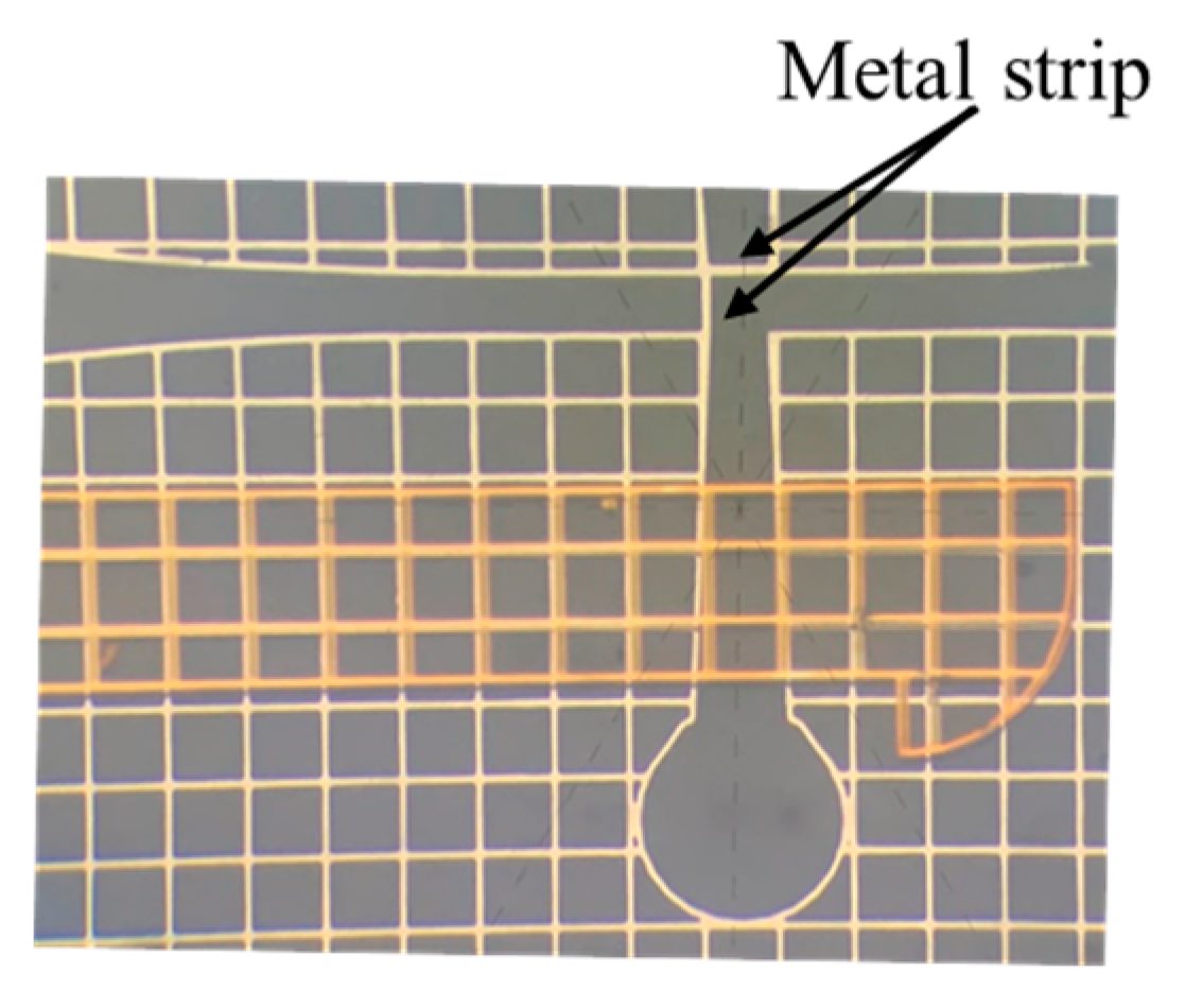
To achieve beam tilt in three specific orientations, namely, state 1, state 2, and state 3, different configurations utilizing a metal strip were employed as depicted in Figure 1a.
State 1 is attained by establishing a connection between petal 1 and petal 2 with the ground plane.
In state 2, petal 2 is connected to both the ground plane and petal 1.
State 3 involves connecting petal 1 to both the ground plane and petal 2.

3. Simulations Results for Opaque Passive Antenna

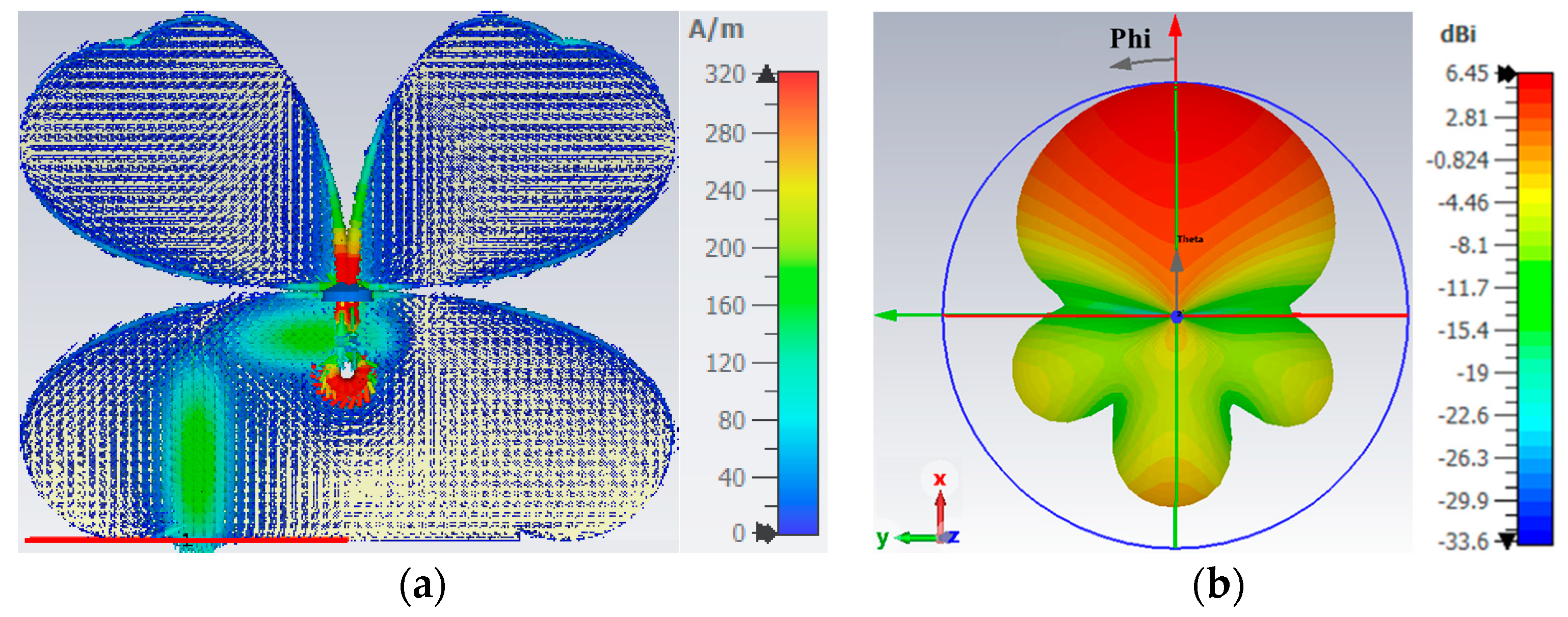
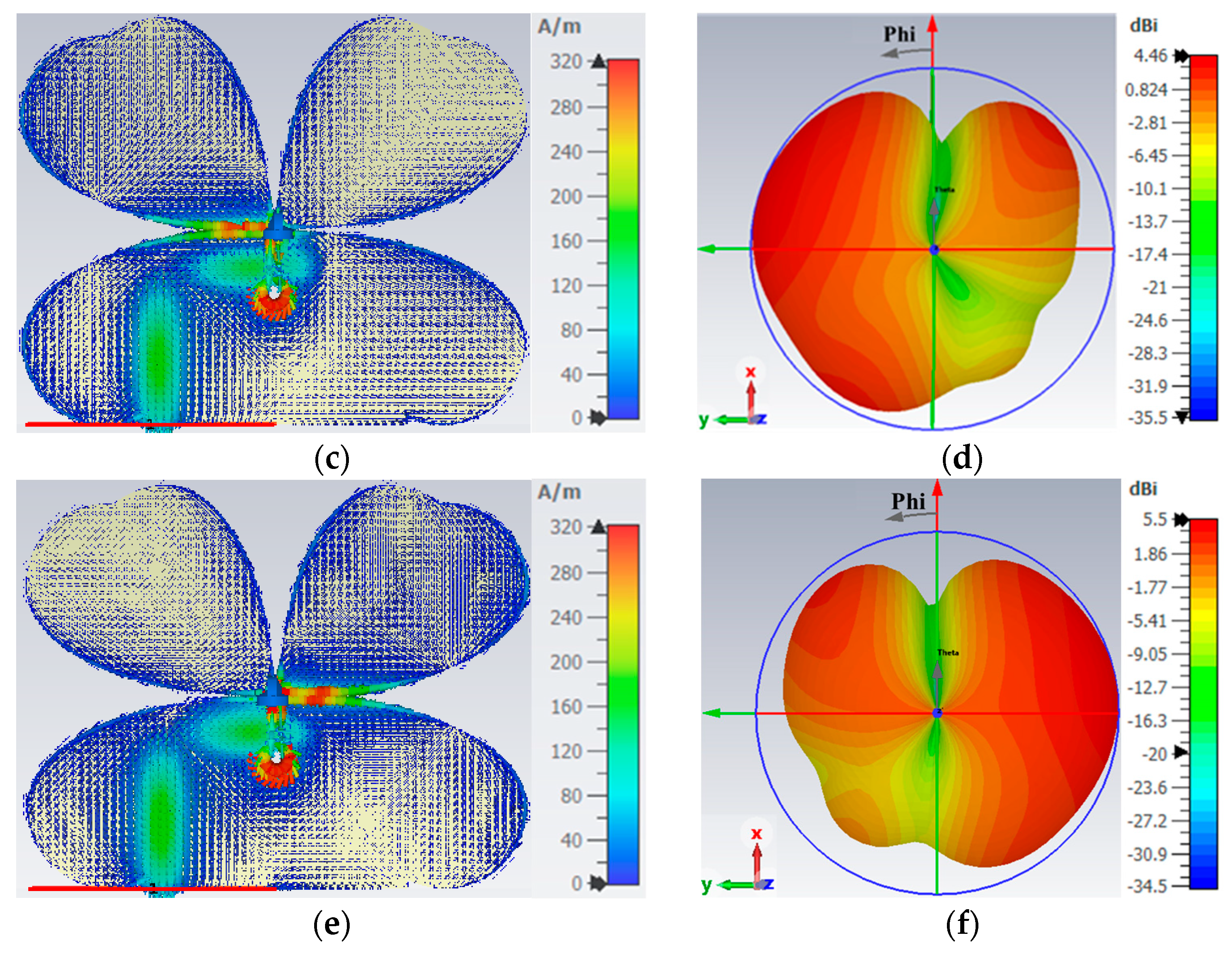
The tapered slots exhibit maximum current flow at their edges, as observed in Figure 2a,c,e. By controlling the current direction, the radiating beam can be adjusted accordingly. In state 1, the beam is radiated at an angle of ϕ = 0° with a peak gain of 6.5 dBi, as depicted in Figure 2b. In state 2, the current deviation occurs on the left side of the tapered slot, resulting in a radiating beam at an angle of ϕ = +90° with a gain of 4.4 dBi, as shown in Figure 2d. Similarly, in state 3, the current deviation occurs on the right side of the tapered slot, resulting in a radiating beam at an angle of ϕ = −90° with a peak gain of 5.5 dBi, as illustrated in Figure 2f.
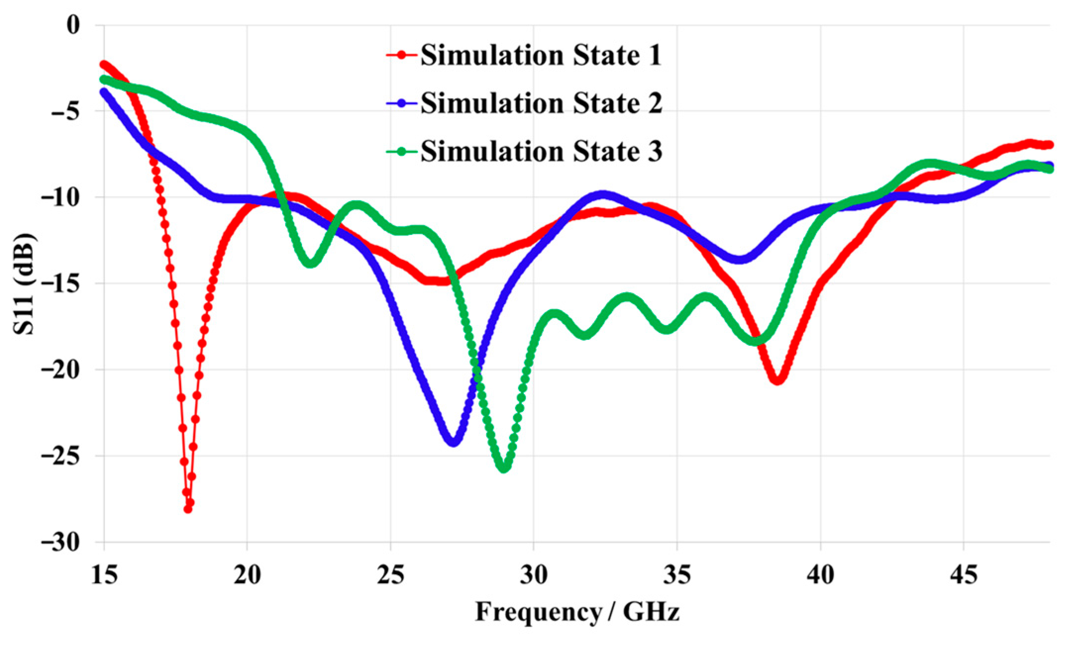
The reflection coefficients of the passive antenna in states 1, 2, and 3 are depicted in Figure 3, showcasing the simulation results. The antenna shows operation within a frequency range from 17 to 42 GHz for state 1, 19 to 45 GHz for state 2, and 21 to 41.5 GHz for state 3, with an S11 magnitude below −10 dB.
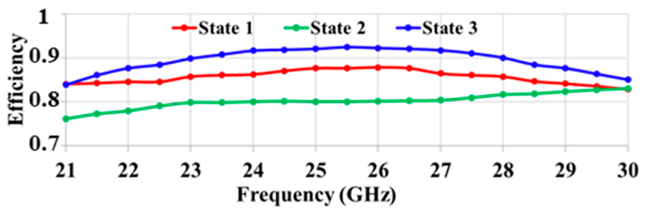
Figure 4 presents the simulation results of the gain. State 1 has a gain of 6.5 dBi at 26 GHz, state 2 has a gain of 4.4 dBi at the same frequency, and state 3 has a gain of 5.5 dBi at 26 GHz. Figure 5 showcases the efficiency performance of the antenna in three distinct states across a frequency range spanning from 21 GHz to 30 GHz.

4. Transparent Vivaldi Antenna Fabrication

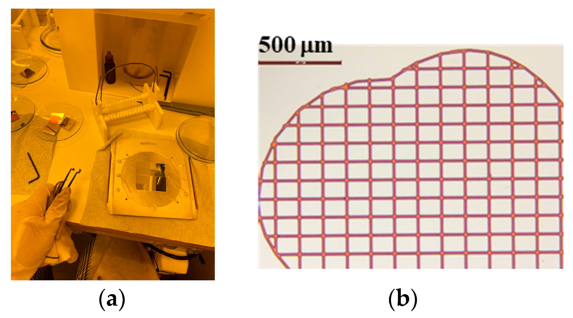
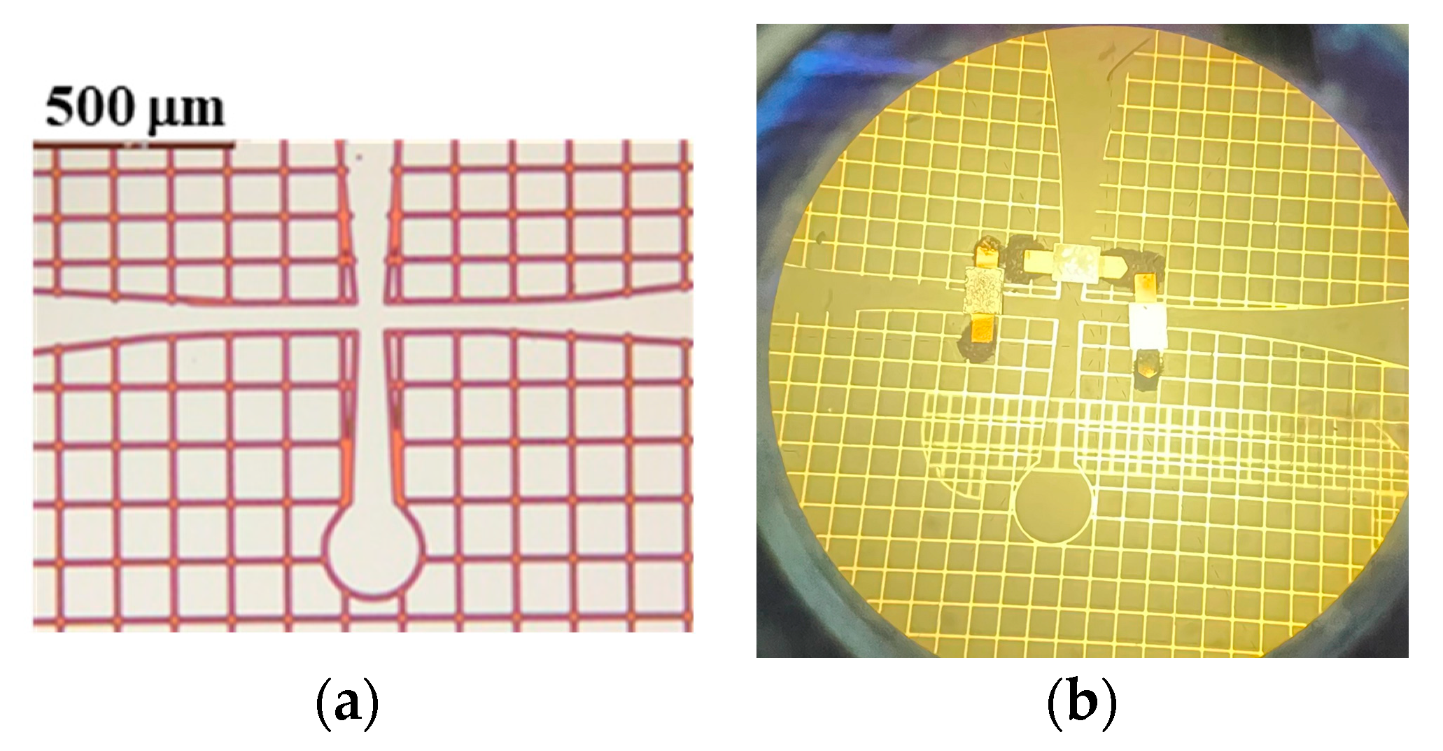
Three transparent mesh antennas have been created using the process described in [28], which involves depositing a 1.35 µm thick continuous silver film and a 5 nm thick titanium adhesion film onto a substrate using RF sputtering. Photolithographic wet etching is then used to create the antenna patterns with appropriate photomasks (Figure 6a). The silver film was made to be three times thicker than the skin depth value (0.45 µm at 26 GHz) using standard photolithographic wet-etching processes and appropriate photomasks. During the photolithography process, the careful alignment of the photomasks and the substrate is crucial to ensure the accuracy of the antenna. The resulting antenna is optically transparent, making it suitable for use in applications where visibility is important, such as in smart windows or heads-up displays. The distance between the antenna elements (pitch) affects the level of optical transparency, with a wider pitch resulting in higher transparency levels (ranging from 66% to 89%). This transparency is measured using a UV–visible spectrophotometer. The process of creating a transparent antenna, illustrated in Figure 6, involves creating square apertures in the metal layers, with a specific pitch and metal strip width. In this case, the pitch is 150 µm and the metal strip width is close to 15 µm. The mesh antenna underwent an optical transparency test using a UV–visible spectrophotometer. The results showed a transparency of 76% across the visible light spectrum of 400–800 nm. This confirms the high optical transparency of the mesh antenna, as shown in Figure 6b. The transparent antenna’s ability to transmit visible light with minimal absorption ensures its suitability for optical applications.

5. Passive Transparent Antenna Results and Discussion

As described in Section 2, metal strips were used in passive antenna designs to achieve beam tilt in three specific orientations (State 1, 2, and 3), as illustrated in Figure 7, which provides an example of the configuration for State 3.
The measurement results presented in Figure 8 demonstrate the performance of the passive transparent antenna in different operating states (1, 2, and 3). The passive transparent prototypes exhibit improved matching compared to the results in Figure 3 for the opaque prototype. This probably occurs due to the presence of a metallic grid with very thin meshes. The antenna shows operation within a frequency range from 15 to 48 GHz for state 1, state 2’s operation occurs from 21 to 48 GHz, and state 3 works from 19 to 45 GHz with an S11 magnitude below −10 dB.

6. Active Transparent Antenna Design

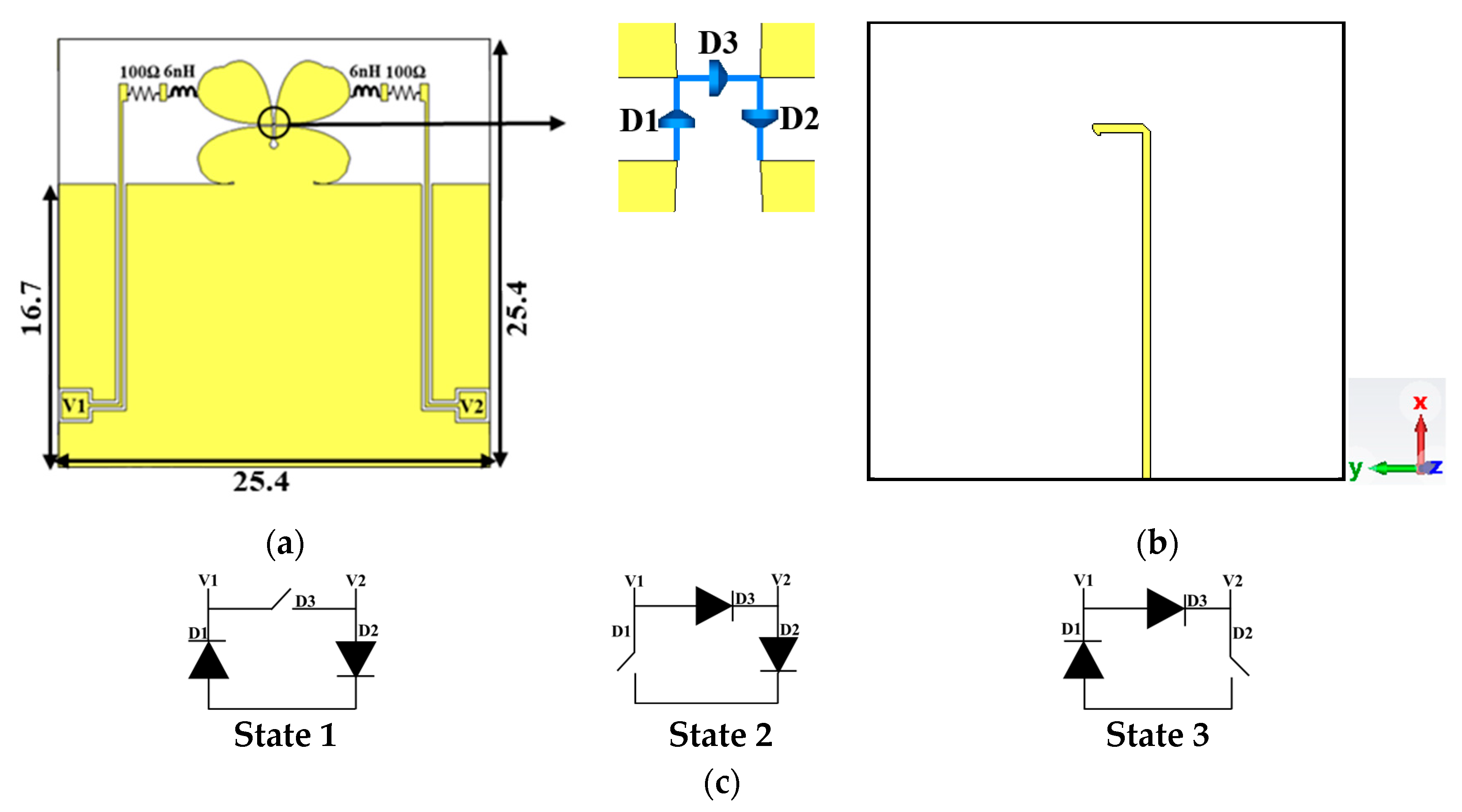
In this section, we will discuss active transparent antennas by substituting the metal strip with active MA4AGP907 diodes, namely, D1, D2, and D3, as shown in Figure 9a. This will enable the antenna to switch between states electronically. Note that the performance of the passive antenna (with metal strip) obtained in the previous sections highlights the losses brought about by the diodes for the active antenna. The three PIN diodes are connected in series in order to use only two DC supply voltages (V1 and V2) for the different states (the configuration is displayed in Table 1). Biasing lines, 200 µm in width, are positioned perpendicularly to minimize their impact on the radiation pattern. Each DC biasing line in the system includes an inductor (L = 6 nH) and resistors (R = 100 Ω) in order to block the RF current and provide protection for the diodes.
State 1 is achieved when D1 and D2 are in the ON state, functioning as a short circuit, while D3 is in the OFF state, acting as an open circuit. State 2 is attained by turning D2 and D3 ON and keeping D1 OFF. Similarly, state 3 is achieved by activating D1 and D3 while keeping D2 OFF. A summary of these states is provided in Table 2.

7. Active Transparent Antenna Results and Discussion

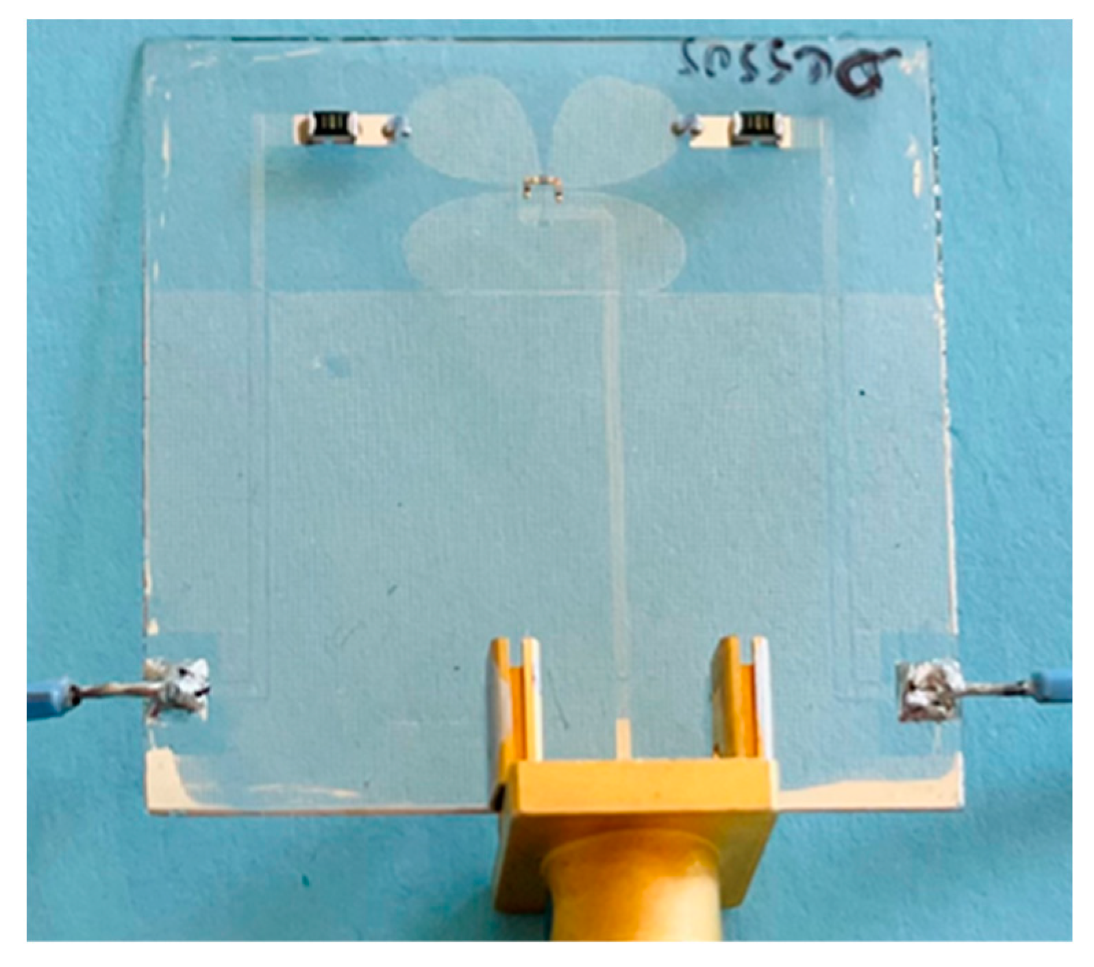
The fabrication method for the transparent antenna was showcased in Section 4. The technique and procedure for achieving transparency in the antenna remain consistent, with the only distinction being the utilization of individual masks for each antenna. It is important to note that, in the case of the active antenna, diodes are employed in place of the metallic strip. The fabricated active antenna is presented in Figure 10.
Figure 11a presents a detailed view of the central section of the transparent antenna before the PIN diodes are installed. In contrast, Figure 11b illustrates the identical region after the diodes have been incorporated.
Figure 12 provides a close-up view of the biasing section used for the active transparent antenna. It utilizes a DC-feed inductor and resistor protection mechanism.
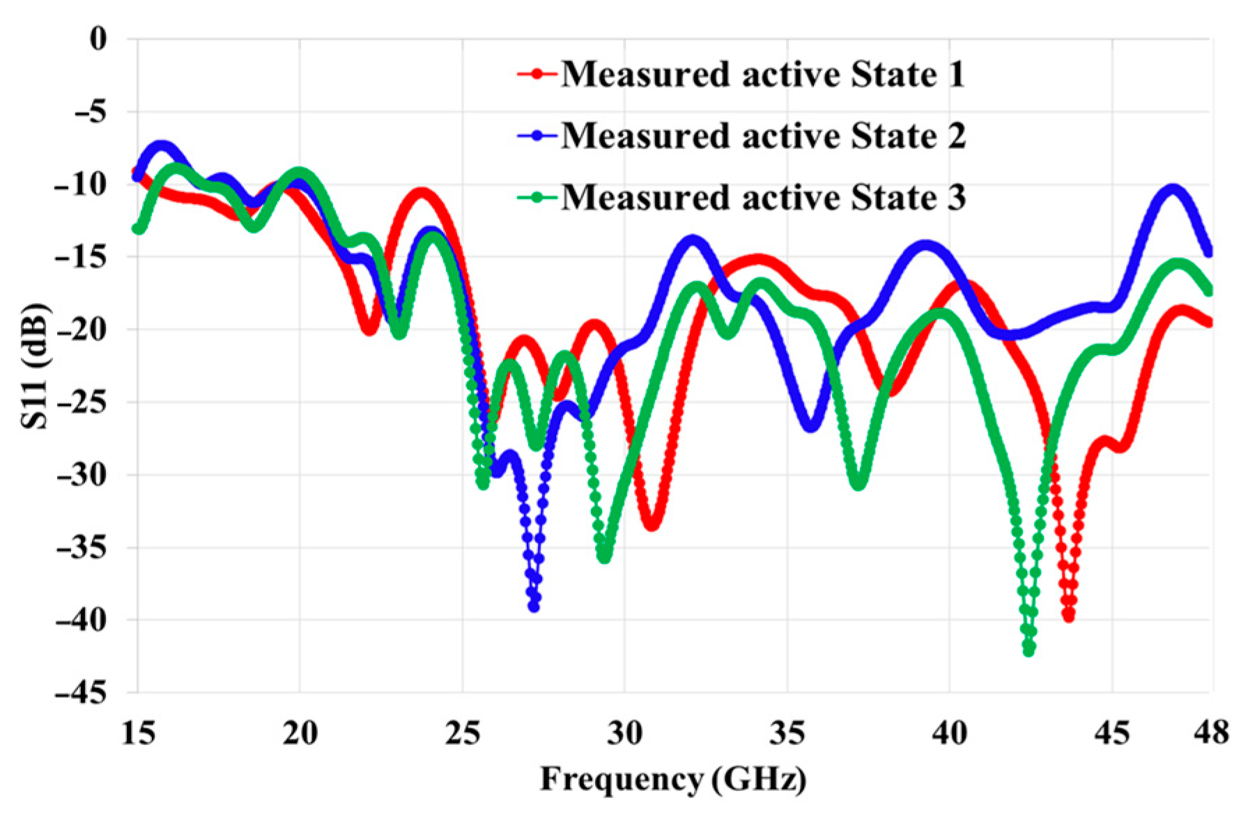
To assess the performance of the active transparent antenna, we present the return losses depicted in Figure 13. It is worth mentioning that the experimental measurements exhibit fluctuations or ripples, which could be attributed to potential errors in the measurement process.
The active transparent prototypes demonstrate improved matching compared to the results shown in Figure 3 for the opaque passive antenna and Figure 8 for the transparent passive antenna. This enhancement could be attributed to the inclusion of PIN diodes and their associated losses. The antennas show a capacity to operate within a frequency range from approximately 15 to 48 GHz for state 1, with a range from 17 to 48 GHz for states 2 and 3.
As depicted in Figure 14, the radiation pattern orientation can be altered as anticipated by adjusting the DC bias of the diodes.
Figure 15 showcases the gain results for each state of the antenna, presenting a comprehensive overview that includes both the measured and simulated outcomes.
In the simulation, state 1 exhibits a gain of 6.5 dBi at 26 GHz, while the measured gain at the same frequency is 6.7 dBi. For state 2, the simulation shows a gain of 4.4 dBi, whereas the measured gain is 4 dBi. In the case of state 3, the simulation yields a gain of 5.5 dBi, while the measured gain is 5.1 dBi, with both detected at the same frequency. The variation in gain can be attributed to the increased level of rear radiation in states 2 and 3. Importantly, the comparison between the simulated and measured results demonstrates good agreement.

8. States Combination

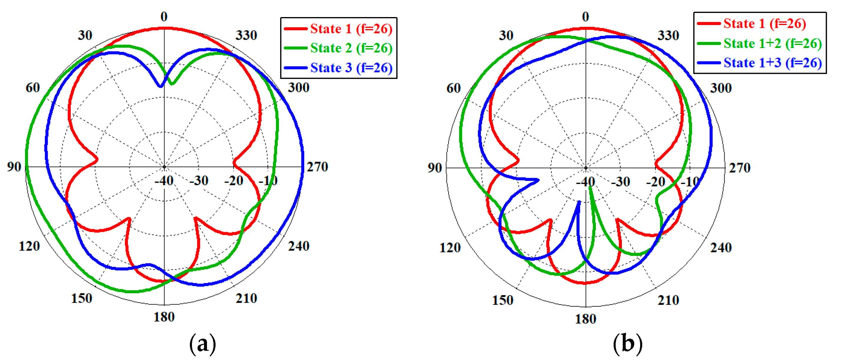
In the first configuration, as shown in Figure 16a, the diode states are switched to achieve a coverage angle of 300° using only three states.
In the second configuration, depicted in Figure 16b, by combining state 1 with either state 2 or state 3, we can create two different options for tilting the beam of state 1, allowing for a beam tilt range of −45° to +45°.

9. Effect of PIN Diode Equivalent Resistor on the Beamwidth Control

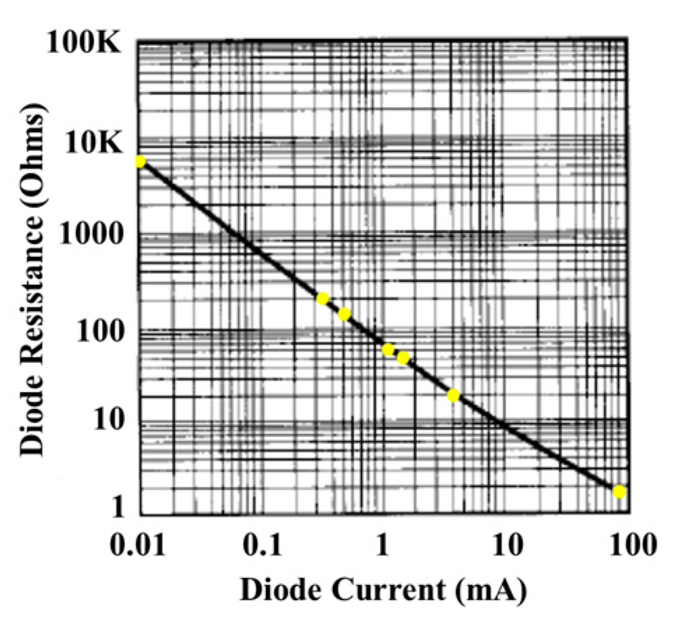
The radiation beams emitted in state 1 exhibit higher directionality compared to the other two states. This is attributed to the ground plane’s improved reflectivity in state 1. In order to achieve a balanced radiation performance across all states in our proposed structure, we adjusted the bias values of the PIN diodes to function as variable resistors. The dynamic resistor characteristics, a function of DC bias, are illustrated in Figure 17.
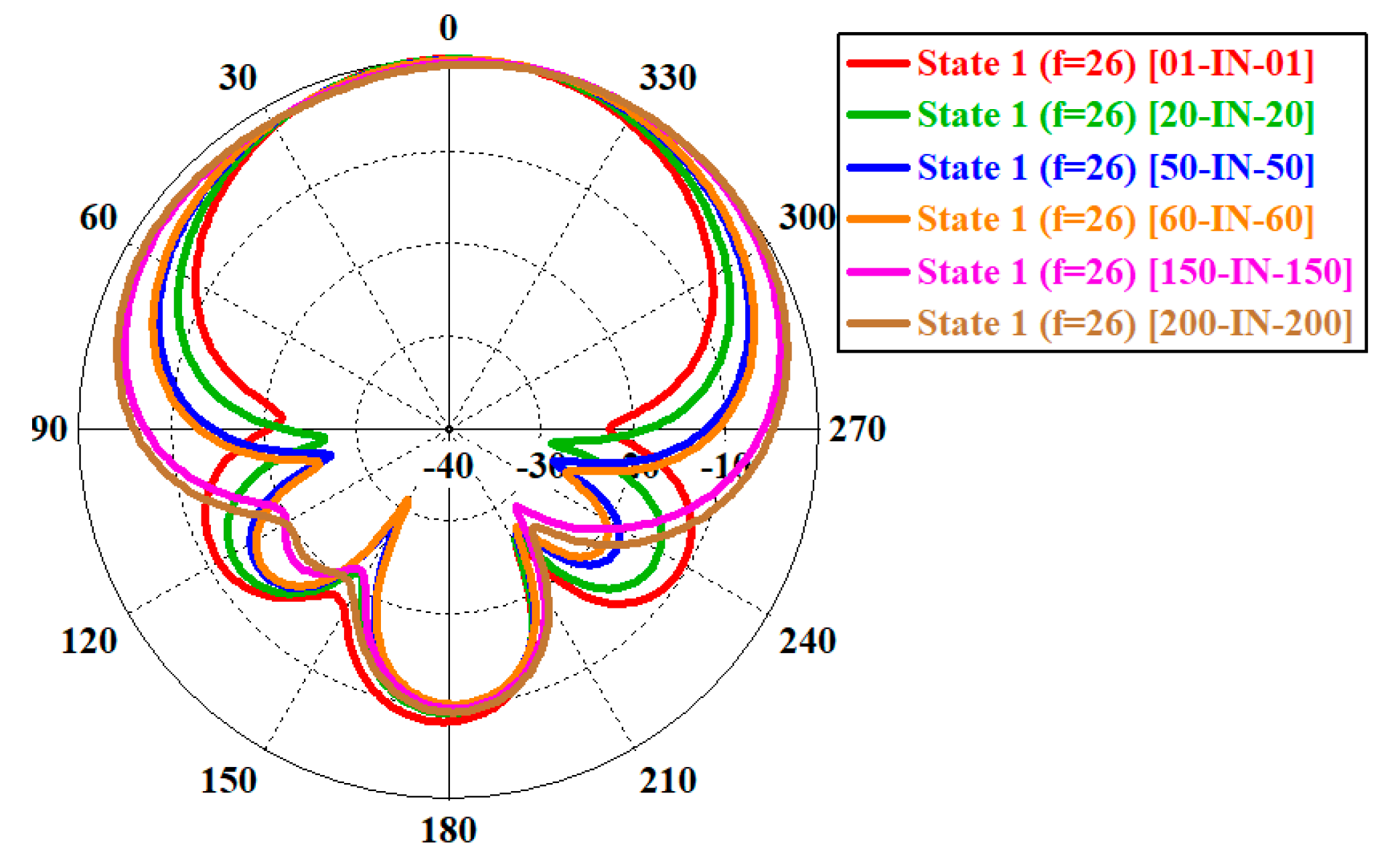
The radiation patterns of state 1 are compared with the different diode biasing configurations in state 3. In the notion X-IN-X, X represents the value of the equivalent resistor diode, while IN denotes an infinite value of the equivalent diode resistor (>6000 Ω for no bias).
According to Figure 18, we have the ability to regulate the aperture of the beam. When the resistor value is X = 0.01 Ω, the beamwidth is 75° at −3 dB. Conversely, when the resistor value is 200 Ω, the beam aperture increases to 155°, which is approximately twice the level of the previous value. Table 3 illustrates the values of the resistors and their corresponding −3 dB beamwidth angles. The same behavior can be applied to states 2 and 3.
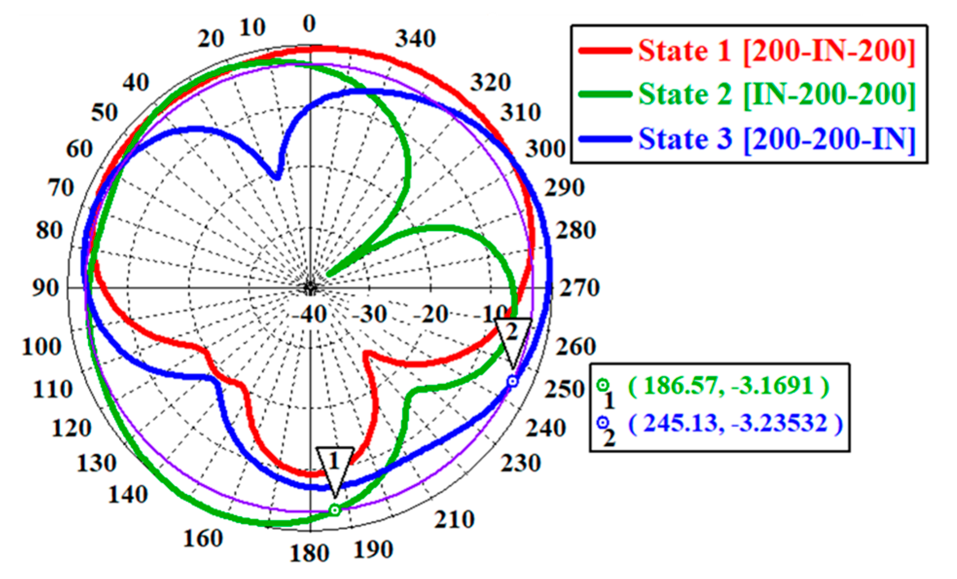
Section 8 demonstrates that, with regard to configuration 1, the coverage can be further increased by controlling the diode resistor states. Additionally, a null value can be created in a specific direction. For example, this occurs in state 2 (IN-200-200, that mean IN > 6000 Ω, and 200 Ω), while state 1 or state 3 exhibit a maximum response at a 305° direction, as illustrated in Figure 19. The purple curve correspond to −3 dB reference level indicator. This configuration can be particularly useful in applications such as direction of arrival (DOA) estimation.
Table 4 provides a summary of all of the configuration cases. Configurations 8 to 10 offer significant control over the beamwidth.
Table 5 provides a comparison between the presented antennas and recently published pattern-reconfigurable antennas. In [6], four PIN diodes were used to achieve nine states, but the coverage was limited to 30°. Ref. [13] used three PIN diodes but achieved only two distinct states and covered just conical and broadside aspects. In [15], the authors achieved a coverage angle of 360° but utilized 12 PIN diodes. In [16,17], the antennas are larger in size compared to this design, have only four working modes, and cover only 6.7% of bandwidth in [16] and 34% in [17]. Similarly, ref. [23] used 16 PIN diodes to cover only 22.5°. In [24], the authors also employed 16 PIN diodes to achieve 8% on bandwidth and a coverage of only 45°. In contrast, our design successfully achieved more than 10 states, with just 3 diodes used as ON/OFF switches and variable resistors.
In [32], the authors presented a similar design to this work, albeit using a non-transparent substrate (Rogers) with an opaque structure. Additionally, they did not propose any control of the beam tilt (which only has 3 directions), beamwidth control, or state combination.
In [33], the authors used a liquid metal to switch between four states, but the antenna achieved a coverage of only 30°.
In [35], the authors used 6 PIN diodes and 12 states but achieved a coverage of only 30°. Finally, in [34], four PIN diodes were utilized to cover 90°.
Therefore, the presented design offers optical transparency, making it suitable for integration into various applications such as smart windows and smart glasses without compromising the device’s appearance. It boasts a wideband antenna (66.7% bandwidth), more than 10 states for beam control, and allows for a coverage of 300° with just 3 PIN diodes.

10. Conclusions

This study introduces a transparent wideband Vivaldi antenna that offers more than 10 state pattern reconfigurabilities. This is achieved by utilizing three PIN diodes, enabling control over beam switching, beamwidth, and beam direction in the horizontal plane. The antenna operates within the frequency range of 18–45 GHz, providing a fractional bandwidth of 66.7%. Notably, the antenna exhibits a transparency level of 76% across the visible light spectrum. Furthermore, the antenna is able to cover 300° with 80% efficiency within the targeted 5G frequency band from 24 to 28 GHz.

Author Contributions

Conceptualization, A.C. and M.H.; methodology, A.C. and M.H.; software, A.C.; validation, A.C. and M.H.; investigation, A.C. and M.H.; data curation, A.C.; writing—original draft preparation, A.C.; writing—review and editing, A.C., M.H., X.C., Q.S., S.D. and F.C.; visualization, supervision, M.H.; project administration, M.H. All authors have read and agreed to the published version of the manuscript.

Funding

This research received no external funding.

Institutional Review Board Statement

Not applicable.

Informed Consent Statement

Not applicable.

Data Availability Statement

Not applicable.

Acknowledgments

This work is supported by the European Union through the European Regional Development Fund (ERDF), the Ministry of Higher Education and Research, the Région Bretagne, the Département des Côtes d’Armor and Saint-Brieuc Armor Agglomération, through the CPER Projects 2015–2020 MATECOM and SOPHIE/STIC & Ondes.

Conflicts of Interest

The authors declare no conflict of interest.

References

  1. Li, Q.C.; Niu, H.; Papathanassiou, A.T.; Wu, G. 5G Network Capacity: Key Elements and Technologies. IEEE Veh. Technol. Mag. 2014, 9, 71–78. [Google Scholar] [CrossRef]
  2. Ilderem, V. 1.4 5G Wireless Communication: An Inflection Point. In Proceedings of the IEEE International Solid-State Circuits Conference-(ISSCC), San Francisco, CA, USA, 17–21 February 2019; pp. 35–39. [Google Scholar]
  3. Dahlman, E.; Parkvall, S.; Skold, J. 4G, LTE-Advanced Pro and the Road to 5G, 3rd ed.; Academic Press: Cambridge, MA, USA, 2016. [Google Scholar]
  4. Tebache, S.; Ghanem, F.; Belouchrani, A. Novel and simple approach for reconfiguring the pattern of an UWB CPW-Fed monopole antenna. In Proceedings of the 2017 Seminar on Detection Systems Architectures and Technologies (DAT), Algiers, Algeria, 20–22 February 2017; pp. 1–5. [Google Scholar]
  5. Soti, S.; Chakravarti, P.K. A comparative analysis on reconfigurable and multiband antennas for 5G and other wireless applications. In Proceedings of the 2021 International Conference on Recent Trends on Electronics, Information, Communication & Technology (RTEICT), Bangalore, India, 27–28 August 2021; pp. 918–922. [Google Scholar]
  6. Jusoh, M.; Aboufoul, T.; Sabapathy, T.; Alomainy, A.; Kamarudin, M.R. Pattern-Reconfigurable Microstrip Patch Antenna with Multidirectional Beam for WiMAX Application. IEEE Antennas Wirel. Propag. Lett. 2014, 13, 860–863. [Google Scholar] [CrossRef]
  7. Abijuru, D.; Hamid, M.; Obadiah, A.N. Improved Vivaldi antenna with radiation pattern control features. Telkomnika 2018, 16, 1143–1149. [Google Scholar] [CrossRef]
  8. Guo, J.; Xiao, S.; Liao, S.; Wang, B.-Z.; Xue, Q. Dual-Band and Low-Profile Differentially Fed Slot Antenna for Wide-Angle Scanning Phased Array. IEEE Antennas Wirel. Propag. Lett. 2017, 17, 259–262. [Google Scholar] [CrossRef]
  9. Sandhu, A.I.; Arnieri, E.; Amendola, G.; Boccia, L.; Meniconi, E.; Ziegler, V. Radiating Elements for Shared Aperture Tx/Rx Phased Arrays at K/Ka Band. IEEE Trans. Antennas Propag. 2016, 64, 2270–2282. [Google Scholar] [CrossRef] [Green Version]
  10. Tekkouk, K.; Hirokawa, J.; Sauleau, R.; Ettorre, M.; Sano, M. Dual-Layer Ridged Waveguide Slot Array Fed by a Butler Matrix with Sidelobe Control in the 60-GHz Band. IEEE Trans. Antennas Propag. 2015, 63, 3857–3867. [Google Scholar] [CrossRef]
  11. Manzillo, F.F.; Smierzchalski, M.; Le Coq, L.; Ettorre, M.; Aurinsalo, J.; Kautio, K.T.; Lahti, M.S.; Lamminen, A.E.I.; Saily, J.; Sauleau, R. A Wide-Angle Scanning Switched-Beam Antenna System in LTCC Technology with High Beam Crossing Levels for V-Band Communications. IEEE Trans. Antennas Propag. 2018, 67, 541–553. [Google Scholar] [CrossRef]
  12. Brookner, E. Practical Phased-Array Antenna Systems; Artech House: Norwood, MA, USA, 1991. [Google Scholar]
  13. Lin, W.; Wong, H.; Ziolkowski, R.W. Wideband Pattern-Reconfigurable Antenna with Switchable Broadside and Conical Beams. IEEE Antennas Wirel. Propag. Lett. 2017, 16, 2638–2641. [Google Scholar] [CrossRef]
  14. Wang, J.; Yin, J.; Wang, H.; Yu, C.; Hong, W. Wideband U-slot patch antenna with reconfigurable radiation pattern. In Proceedings of the 2017 11th European Conference on Antennas and Propagation (EUCAP), Paris, France, 19–24 March 2017; pp. 611–615. [Google Scholar]
  15. Yang, Y.; Zhu, X. A Wideband Reconfigurable Antenna With 360° Beam Steering for 802.11ac WLAN Applications. IEEE Trans. Antennas Propag. 2018, 66, 600–608. [Google Scholar] [CrossRef]
  16. Alam, M.S.; Abbosh, A.M. Beam-Steerable Planar Antenna Using Circular Disc and Four PIN-Controlled Tapered Stubs for WiMAX and WLAN Applications. IEEE Antennas Wirel. Propag. Lett. 2015, 15, 980–983. [Google Scholar] [CrossRef]
  17. Alam, M.S.; Abbosh, A.M. Wideband Pattern-Reconfigurable Antenna Using Pair of Radial Radiators on Truncated Ground with Switchable Director and Reflector. IEEE Antennas Wirel. Propag. Lett. 2016, 16, 24–28. [Google Scholar] [CrossRef]
  18. Zhu, S.; Liu, H.; Chen, Z.; Wen, P. A Compact Gain-Enhanced Vivaldi Antenna Array with Suppressed Mutual Coupling for 5G mmWave Application. IEEE Antennas Wirel. Propag. Lett. 2018, 17, 776–779. [Google Scholar] [CrossRef]
  19. Malakooti, S.-A.; Moosazadeh, M.; Ranasinghe, D.C.; Fumeaux, C. Antipodal Vivaldi Antenna for Sum and Difference Radiation Patterns with Reduced Grating Lobes. IEEE Antennas Wirel. Propag. Lett. 2017, 16, 3139–3142. [Google Scholar] [CrossRef]
  20. Tianang, E.G.; Elmansouri, M.A.; Filipovic, D.S. Ultra-Wideband Lossless Cavity-Backed Vivaldi Antenna. IEEE Trans. Antennas Propag. 2017, 66, 115–124. [Google Scholar] [CrossRef]
  21. Ren, X.; Liao, S.; Xue, Q. Design of Wideband Circularly Polarized Vivaldi Antenna with Stable Radiation Pattern. IEEE Access 2017, 6, 637–644. [Google Scholar] [CrossRef]
  22. Dong, Y.; Choi, J.; Itoh, T. Vivaldi Antenna with Pattern Diversity for 0.7 to 2.7 GHz Cellular Band Applications. IEEE Antennas Wirel. Propag. Lett. 2018, 17, 247–250. [Google Scholar] [CrossRef]
  23. Yang, Y.; Simorangkir, R.B.V.B.; Zhu, X.; Esselle, K.; Xue, Q. A Novel Boresight and Conical Pattern Reconfigurable Antenna with the Diversity of 360° Polarization Scanning. IEEE Trans. Antennas Propag. 2017, 65, 5747–5756. [Google Scholar] [CrossRef]
  24. Chen, S.-L.; Qin, P.-Y.; Lin, W.; Guo, Y.J. Pattern-Reconfigurable Antenna with Five Switchable Beams in Elevation Plane. IEEE Antennas Wirel. Propag. Lett. 2018, 17, 454–457. [Google Scholar] [CrossRef] [Green Version]
  25. Yasin, T.; Baktur, R.; Furse, C. A study on the efficiency of transparent patch antennas designed from conductive oxide films. In Proceedings of the 2011 IEEE International Symposium on Antennas and Propagation (APSURSI), Spokane, WA, USA, 3–8 July 2011; pp. 3085–3087. [Google Scholar]
  26. Colombel, F.; Cruz, E.M.; Himdi, M.; Legeay, G.; Castel, X.; Vigneron, S. Ultrathin metal layer, ITO film and ITO/Cu/ITO multilayer towards transparent antenna. IET Sci. Meas. Technol. 2009, 3, 229–234. [Google Scholar] [CrossRef]
  27. Peter, T.; Yuk, T.; Nilavalan, R.; Cheung, S. A novel technique to improve gain in transparent UWB antennas. In Proceedings of the 2011 Loughborough Antennas & Propagation Conference, Loughborough, UK, 14–15 November 2011; pp. 1–4. [Google Scholar]
  28. Hautcoeur, J.; Castel, X.; Colombel, F.; Benzerga, R.; Himdi, M.; Legeay, G.; Motta-Cruz, E. Transparency and electrical properties of meshed metal films. Thin Solid Films 2011, 519, 3851–3858. [Google Scholar] [CrossRef]
  29. Castel, X.; Himdi, M.; Colombel, F. Comparison of the microwave performance of transparent monopole antennas made of different transparent conducting films. In Proceedings of the IEEE Conference on Antenna Measurements & Applications (CAMA), Västeras, Sweden, 3–6 September 2018. [Google Scholar]
  30. Elmobarak Elobaid, H.A.; Abdul Rahim, S.K.; Himdi, M.; Castel, X.; Abedian Kasgari, M. A Transparent and Flexible Polymer-Fabric Tissue UWB Antenna for Future Wireless Networks. IEEE Antennas Wirel. Propag. Lett. 2017, 16, 1333–1336. [Google Scholar] [CrossRef]
  31. Martin, A.; Gautier, C.; Castel, X.; Himdi, M. Transparent and miniature FM antenna in printed technology. Int. J. Microw. Wirel. Technol. 2018, 10, 19–24. [Google Scholar] [CrossRef]
  32. Cherif, A.; Himdi, M.; Dakhli, S.; Castel, X.; Choubani, F. Broadband Reconfigurable Vivaldi Antenna for 5G Communication. In Proceedings of the 2022 IEEE 22nd Annual Wireless and Microwave Technology Conference (WAMICON), Clearwater, FL, USA, 27–28 April 2022; pp. 1–4. [Google Scholar]
  33. Bai, X.; Su, M.; Liu, Y.; Wu, Y. Wideband Pattern-Reconfigurable Cone Antenna Employing Liquid-Metal Reflectors. IEEE Antennas Wirel. Propag. Lett. 2018, 17, 916–919. [Google Scholar] [CrossRef]
  34. Lu, Z.-L.; Yang, X.-X.; Tan, G.-N. A Wideband Printed Tapered-Slot Antenna with Pattern Reconfigurability. IEEE Antennas Wirel. Propag. Lett. 2014, 13, 1613–1616. [Google Scholar] [CrossRef]
  35. Towfiq, A.; Bahceci, I.; Blanch, S.; Romeu, J.; Jofre, L.; Cetiner, B.A. A Reconfigurable Antenna with Beam Steering and Beamwidth Variability for Wireless Communications. IEEE Trans. Antennas Propag. 2018, 66, 5052–5063. [Google Scholar] [CrossRef] [Green Version]
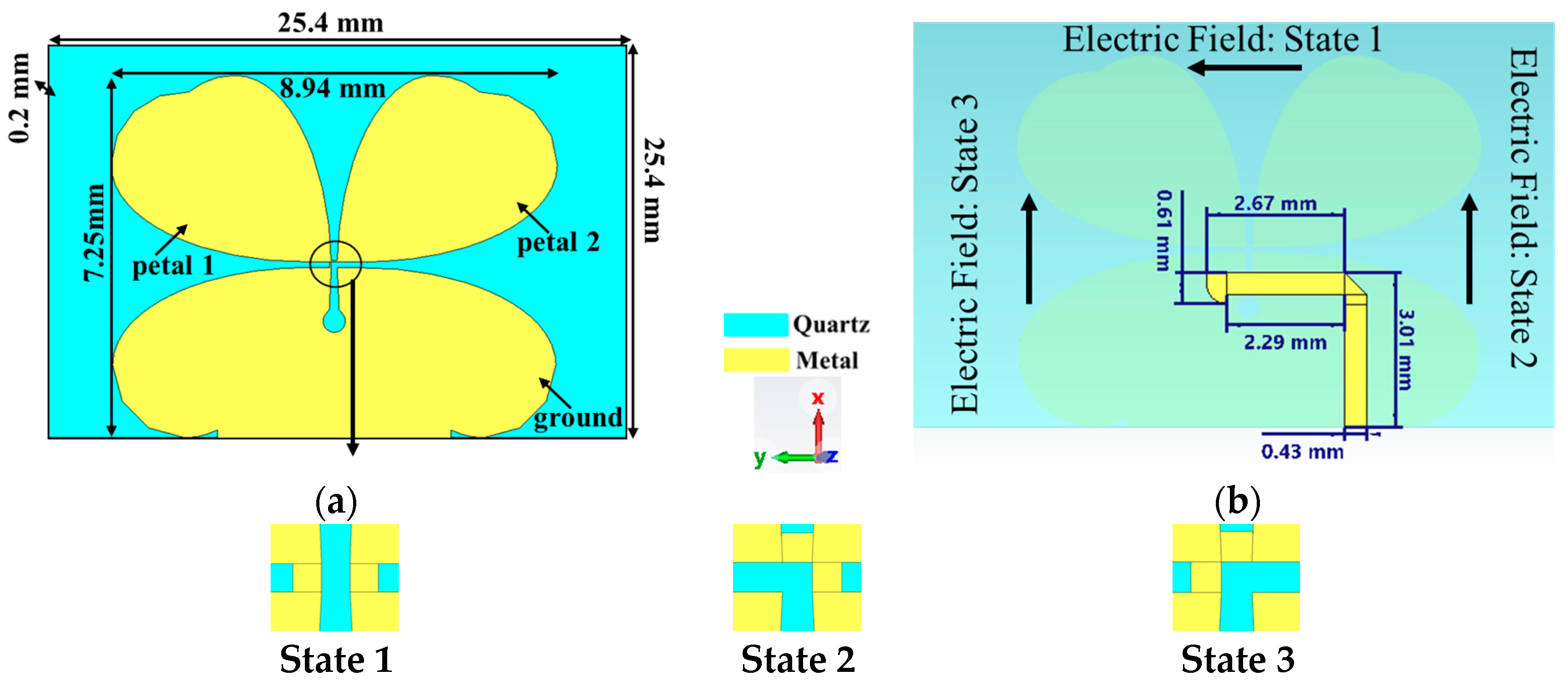
Figure 1. Configuration and geometries of the passive antenna: (a) front side with metallic strips as short circuit for different states; (b) back side with feeding microstrip line.
Applsci 13 07878 g001
Figure 2. The current surface distribution: (a) state 1, (c) state 2, (e) and state 3. The 3D radiation pattern at 26 GHz: (b) state 1, (d) state 2, and (f) state 3.
Applsci 13 07878 g002aApplsci 13 07878 g002b
Figure 3. Simulations of reflection coefficient of the passive antenna operating in states 1, 2, and 3.
Applsci 13 07878 g003
Figure 4. Simulated gain of the three states of the opaque passive Vivaldi antenna.
Applsci 13 07878 g004
Figure 5. Efficiency of the opaque passive Vivaldi antenna operating in states 1, 2, and 3.
Applsci 13 07878 g005
Figure 6. Fabricated transparent Vivaldi antenna: (a) clean room, zoomed view by optical microscopy (scale bar = 500 μm); (b) a mesh petal.
Applsci 13 07878 g006
Figure 7. Passive transparent antenna (example of the antenna in state 3).
Applsci 13 07878 g007
Figure 8. Measured return losses of the transparent passive antenna.
Applsci 13 07878 g008
Figure 9. Feeding strategy and geometries of the active antenna: (a) front side, (b) back side, and (c) diodes’ states.
Applsci 13 07878 g009
Figure 10. The active transparent antenna that has been fabricated.
Applsci 13 07878 g010
Figure 11. Zoomed view using an optical microscope. Mesh ground with the petals (a) before the implementation of the diodes, (b) after the implementation of the diodes.
Applsci 13 07878 g011
Figure 12. The positions of the inductor and resistor in the fabricated active antenna.
Applsci 13 07878 g012
Figure 13. Return losses of the transparent active antenna.
Applsci 13 07878 g013
Figure 14. Measured radiation patterns Eφ versus φ of active transparent antenna operating in (a) state 1, (b) state 2, and (c) state 3 at frequencies of 26, 27, and 28 GHz.
Applsci 13 07878 g014
Figure 15. A comparison of the gain between simulations and measurements for the active transparent antenna operating in states 1, 2, and 3.
Applsci 13 07878 g015
Figure 16. (a) Polar plot of all three states (Eφ versus φ). (b) Combination of state 1 results in a change in the direction of the beam (Eφ versus φ).
Applsci 13 07878 g016
Figure 17. Diode resistance versus DC diode curent polarization. The yellow circles correspond to values of 6000, 200, 150, 60, 50, 20, and 0.01 ohms.
Applsci 13 07878 g017
Figure 18. State 1 exhibits varying diode resistor values (Eφ versus φ).
Applsci 13 07878 g018
Figure 19. Coverage enhancement using state 1, state 2, and state 3 with special diode resistor values (Eφ versus φ).
Applsci 13 07878 g019
Table 1. Configuration states.
StatesV1V2
State 1>0<0V1 > V2V1 = 2.9 V, V2 = −2.9 V
State 2<0<0V1 < V2V1 = −4.3 V, V2 = −2.9 V
State 3>0>0V1 < V2V1 = 2.9 V, V2 = 4.3V
Table 2. Diodes’ states.
StateD1D2D3
State 1ONONOFF
State 2OFFONON
State 3ONOFFON
Table 3. The summary of −3 dB beamwidth controlled by equivalent resistor diodes D2 and D3 while D3 is off (high equivalent resistor value).
R = R2 = R3θ−3dB
075
2084
5099
60104
150145
200155
Table 4. Summarized Configuration states.
ConfigurationStateD1D2D3Beam Characteristic
1State 1ONONOFFBroadside 0°
2State 2OFFONON+90° left
3State 3ONOFFON−90° right
4State 4OFFOFFOFFlarge
5State 1 + 2OFFOFFON+45° tilt
6State 1 + 3OFFONOFF−45° tilt
7State 2 + 3ONOFFOFFBidirectional ±90°
8State 1
(R1-IN-R2)
Variable diode equivalent
resistor R1
Variable diode equivalent
resistor R2
OFF Control of beamwidth around 0°
9State 2
(IN-R3-R2)
OFFVariable diode equivalent
resistor R2
Variable diode equivalent
resistor R3
Control of beamwidth around +90°
10State 3
(R1-R3-IN)
Variable diode equivalent
resistor R1
OFFVariable diode equivalent
resistor R3
Control of beamwidth around −90°
Table 5. Beam switching and bandwidth improvement design summary.
Ref.AntennaMethodRF
Component
BW
(%)
No. of StatesCoverage
Angle
Gain (dBi)
[6]PatchParasitic tuning4 PIN diodes0.6930°7
[13]Patch Parasitic tuning 3 PIN diodes 23.5 2Conical/broadside6.9–8.2
[15]PatchParasitic tuning12 PIN diodes14.56360°10
[16]PlanarSwitchable stubs4 PIN diodes6.1490°5
[17]Monopole Multiple radiators 4 PIN diodes 34 490° 2.8–3.7
[23]PatchMultiple radiators16 PIN diodes2.61622.5°4.4–6
[24]Dipole Parasitic tuning 16 PIN diodes8 545° 5.2–6.5
[32]Triple
Vivaldi
Non-transparent microstrip line 3 PIN diode703300°5.5
[33]Cone Parasitic reflectors Liquid metal 45.5 4 30° 6.7
[34]Tapered slot Multiple radiators 4 PIN diodes 71 290° 6.4
[35]Patch Parasitic tuning 6 PIN diodes29 1230° 8
This workTriple
Vivaldi
Transparent
microstrip line
3 PIN diodes66.710300°6.45
Disclaimer/Publisher’s Note: The statements, opinions and data contained in all publications are solely those of the individual author(s) and contributor(s) and not of MDPI and/or the editor(s). MDPI and/or the editor(s) disclaim responsibility for any injury to people or property resulting from any ideas, methods, instructions or products referred to in the content.