Abstract
In this paper, we propose a new hardware algorithm for an integer based discrete cosine transform (IntDCT) that was designed to allow an efficient VLSI implementation of the discrete cosine transform using the systolic array architectural paradigm. The proposed algorithm demonstrates multiple benefits specific to integer transforms with efficient hardware implementation and sufficient precision in approximating irrational transform coefficients for practical applications. The proposed integer DCT algorithm can be efficiently restructured into five regular and modular computational structures of lengths of four and one of length two called pseudo-cycle convolutions which translate into efficient VLSI implementations using systolic arrays. Moreover, besides an efficient VLSI implementation with high-speed performances due to the parallel decomposition of the proposed integer DCT algorithm, the proposed VLSI architecture uses a tag control mechanism that facilitates the integration of an obfuscation technique that significantly improves the hardware security with low overheads, maintaining all the implementation performances.
1. Introduction
Multimedia applications involve processing a huge amount of data at a high-speed, thus introducing important challenges to research, especially in mobile devices where the resource usage is constrained. In this context, important research areas that have been developed include image compression, data transmission or Internet of Things, and more. These challenges increase even more for real-time applications, characterized by difficult-to-meet constraints on area, speed, throughput, and power. Audio and video conferencing platforms, digital libraries and archives, remote assistance, and telemedicine are typical applications that push for important developments in this research area. For real-time multimedia applications to support the exigent requirements regarding area, power, and speed performances, the efficient use of the VLSI technology based on reconfigurable FPGA circuits or application-specific integrated circuits (ASICs) is becoming mandatory.
An ubiquitously used transform in data compression and transmission, due to it representing a good approximation of the statistically optimal Karhunen–Loeve transform [1], is the discrete cosine transform (DCT). To accommodate the computationally intensive forward DCT (DCT II) for use in real-time applications, the development of new algorithms or the reformulation of existing ones has become a necessity.
To develop efficient VLSI algorithms, it is important to take into consideration the data flow in the algorithm in the design of new algorithms or the reformulation of existing ones. The performances of a VLSI algorithm are determined even more by the communication complexity and structure and then by its arithmetic complexity. Hence, using regular and modular computational structures can lead to good hardware implementation solutions for the discrete transforms [2,3,4,5,6,7] using systolic arrays [8] or distributed arithmetic [9]. As can be seen, this approach offers reduced hardware complexity with low I/O cost and high speed with good topological features.
It was shown that the VLSI implementation advantages specific to circular correlation or cycle convolution can be extended to other related structures such as pseudo-cycle convolution, band-correlation, skew-circular, and pseudo-circular correlations.
The main VLSI implementations’ advantages of these regular and modular computational structures stem from their particular data flow management, consisting of efficient input/output and data transfer operations, which are successfully utilized in distributed arithmetic systems and systolic arrays.
One important problem in the VLSI implementation of the DCT is that some elements of the transform kernel are irrational, which increases the computational cost and may cause a mismatch between the encoder and decoder as well as drifting errors.
Integer discrete cosine transform (Int-DCT) [10,11] was designed to solve this problem and has been adopted in the recent coding standards such as H.264/Advanced Video Coding (AVC) [12], Audio and Video Streaming (AVS) [13], Video Codec-1 (VC-1) [14], and high-efficiency video coding (HEVC) [15], which uses 4-point to 32-point Int-DCT.
Several 8-point approximated DCTs are proposed in [16,17,18] with different techniques to derive efficient transforms with a lower number of required additions. Larger transforms such as 16-point DCT can offer better performances as more coding gains compared with 4-point or 8-point transforms [19,20,21].
The importance of protecting designs and products has increased nowadays such that the search for measures to protect intellectual property (IP) from counterfeit, malicious alteration, or reverse engineering using hardware security techniques has intensified.
While there are several hardware security solutions, one of the most efficient solutions for improving hardware security is the obfuscation [22,23,24,25,26,27,28].
In this paper, we describe a new integer algorithm for DCT suitable for an efficient hardware implementation of DCT. One aspect of the obtained VLSI algorithm is the possibility to have only multiplications with small integer constants that have low complexity of signed digit representations and can be realized with adders and shift operations. The proposed integer algorithm was decomposed into five pseudo-cycle convolutions of length and one pseudo-cycle convolution of length that can be computed in parallel, leading to a reduced hardware complexity with high processing speeds. The obtained computational structures present the advantages of the cyclic convolution and circular correlation structures-based VLSI. Moreover, the particular tag control mechanism facilitates the efficient integration of the obfuscation technique based on the method introduced in [27].
The main contributions of the paper can be summarized as follows:
- A new Integer DCT matrix is defined which has a high precision and can be efficiently implemented in VLSI;
- The proposed algorithm can be reformulated in a such way that it can be decomposed into five pseudo-cycle convolutions of length four and one of length two;
- It was shown that the derived computational structures can be efficiently implemented using systolic arrays;
- The proposed VLSI algorithm and architecture can efficiently incorporate the obfuscation technique with low overheads and with no impact on the speed performances.
The rest of the paper is organized as follows: in Section 2 we present a new algorithm for Integer DCT with a reduced computational complexity that is using a regular and modular computational structure called pseudo-cycle convolution that is well adapted for an efficient VLSI implementation with similar advantages as cycle-convolution. In Section 3, we present the derived VLSI architecture that emphasizes the advantages of the new Integer DCT algorithm from a VLSI implementation point of view. In Section 4, we discuss the obtained results and it has been shown that a significant reduction in the hardware complexity can be obtained using the proposed Integer DCT algorithm and that it allows the incorporation of the obfuscation technique with low overheads. In Section 5, we are presenting the conclusions.
2. A New VLSI Algorithm for Integer DCT
The 1-D discrete cosine transform (DCT) for a real input sequence is defined as:
The multiplication with the constant can be performed at the end of the VLSI array. An even better solution is to integrate this multiplier in the final design into the quantization stage. For the rest of this work, the multiplication constant will not be taken into consideration.
Using ideas such as those in [10,11], the matrix used for integer DCT is:
We have designed a new integer DCT that can be efficiently implemented using the systolic array architectural paradigm given by the following equation:
To obtain Equation (4), a multi-criterial optimization must be used. A linear integer optimization has been used to search an optimum solution according to the following criteria:
- closeness to the original DCT;
- orthogonality of the basis vector;
- low implementation costs.
These criteria have also been applied in [29,30], but in our case the optimization process was guided to obtain a solution suitable for a systolic array implementation. We have only considered the solution that can lead to a systolic array implementation and we have disregarded the other possible solutions during the optimization process. Naturally, this part of the optimization process cannot be conducted automatically and the know-how of a designer with strong expertise in systolic array architectures is required.
As it can be seen from Equation (4), the matrix coefficients have specific properties, such as symmetric and anti-symmetric properties, that can be exploited for efficient VLSI implementation using systolic arrays.
The obtained integer transform has good accuracy that even outperforms the standard form described by Equation (3), as can be seen in Figure 1.
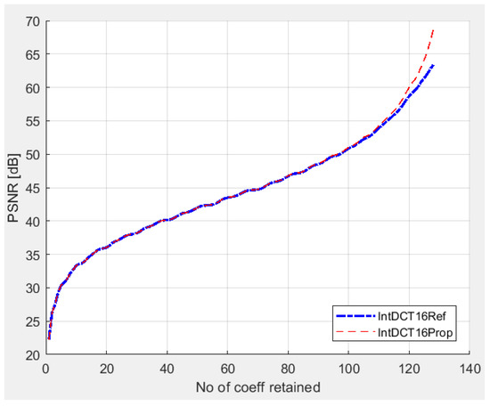
Figure 1.
PSNR for the two Integer algorithms ([10] and proposed).
Figure 1 illustrates the ability of the proposed transform to retain the important features of an image (Lena in our tests) by computing the peak signal-to-noise ratio (PSNR) between the original and the reconstructed image. By varying the number of retained coefficients from low (corresponding to the best image compression) to high (corresponding to the best image quality), one can find the optimum trade-off between compression and quality. For the representation in Figure 1, the same test image and number of bits were used in the simulations to compute the PSNR for the two transforms from Equations (3) and (4).
As shown in Figure 1, the PSNR resulting from using the proposed IntDCT transform, as defined in (4), is identical to the PSNR resulting from using the transform from (3) when the number of retained coefficients is small. This can be explained by the fact that most of the energy is concentrated at low frequencies, for which both Equations (3) and (4) produce identical results. On the other hand, by taking all the coefficients into consideration when reconstructing the original image, the proposed transform in (4) achieves better results with a PSNR of 68 dB compared to 63 dB for the IntDCT from [10], as described by Equation (3).
To obtain an efficient VLSI algorithm, we reformulated (4) by appropriately restructuring and permuting the input and output sequences. Thus, we obtained a parallel form of the algorithm that uses 5 quasi-cycle convolution structures that can operate concurrently.
We introduce the following notations:
Thus, we can write Equation (4) in a matrix–vector product as follows:
By scaled summing the results of the auxiliary sequences and with from Equations (6) and (7), a subset of the output sequence is obtained:
In a similar manner, another subset of the output sequence is obtained by combining the auxiliary results from Equations (9) and (10):
The subset with of the output sequence is obtained directly from the matrix vector product below:
The particular structure of the matrices in Equations (6), (7), (9), (10) and (12), where all the elements along the main diagonal of the matrix or parallel to the main diagonal of the matrix are the same with the exception of the sign, is called a quasi-cycle convolution. This computational structure has an important advantage from a VLSI implementation point of view as it can be efficiently implemented using the systolic array architectural paradigm. As already known, this architecture is very appropriate for efficient VLSI implementation.
The elements and of the output sequence are obtained as follows:
The matrix–vector product from Equation (13) has the same specific form of Equations (6), (7), (9), (10) and (12) but at half the length.
Finally, we can compute and using the following equation:
or, written explicitly:
Therefore, beside the advantages of integer algorithms stemming from efficient implementations of the multipliers, the proposed reformulation allows for an efficient hardware implementation using systolic arrays. Moreover, the obtained algorithm based on quasi-cycle convolution structures and its associated VLSI architecture facilitates the integration of the obfuscation technique.
3. The Proposed VLSI Architecture for the New Integer DCT Algorithm
3.1. Designing the VLSI Architecture
Using the method presented in [31], based on the data dependence graph and the control mechanism described in [32] based on tag bits, Equations (6), (7), (9), (10) and (12) can be mapped to five linear systolic arrays consisting of four processing elements. Furthermore, Equation (13) can be mapped on a similar systolic array that has only two processing elements. The data dependence graph (DDG) was used as the main tool in our design flow together with an appropriate control mechanism based on control tags.
Figure 2 presents the operation of the processing elements of the implemented systolic arrays. All the processing elements have the same functionality, which is an important advantage from a VLSI implementation point of view. Each processing element contains a multiplier by a constant and an adder/subtracter. In Figure 2, sign is a tag control bit that selects the sign of the operation.
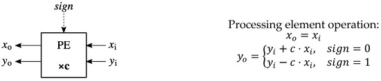
Figure 2.
The function of a processing element (PE) used in the systolic arrays.
The linear systolic arrays from Figure 3, Figure 4, Figure 5, Figure 6 and Figure 7 implement four pseudo-cycle convolution structures with the same structure and which have the same length . The linear systolic array from Figure 8 also implements a pseudo-cycle convolution of length . It can be observed that each processing element contains one multiplier with a small constant that can be implemented using only two adders and shifters, with only one exception where three adders are used to implement the multiplication with such small constants. Thus, the complexity of the processing elements and the delay introduced by these multipliers are significantly reduced.
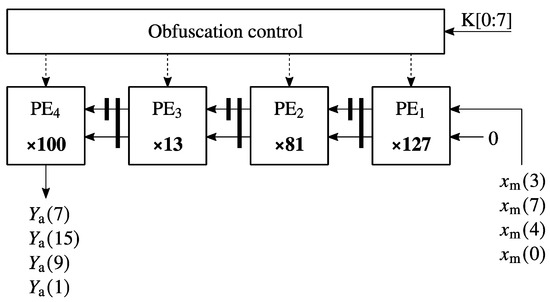
Figure 3.
Systolic array for Equation (6).
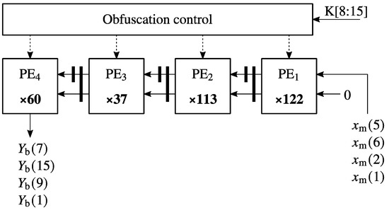
Figure 4.
Systolic array for Equation (7).
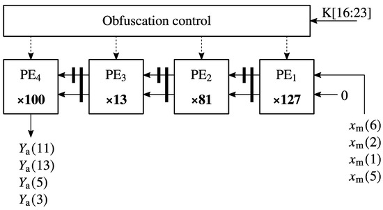
Figure 5.
Systolic array for Equation (9).
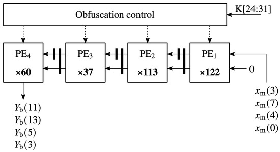
Figure 6.
Systolic array for Equation (10).
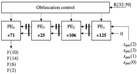
Figure 7.
Systolic array for Equation (12).
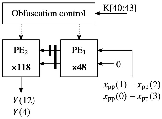
Figure 8.
Systolic array for Equation (13).
Equation (6) was mapped on the systolic array from Figure 3. It can be seen that the systolic array from Figure 3 computes the auxiliary input sequences , , and and the auxiliary outputs , , , and .
Equation (7) was mapped on the systolic array from Figure 4. The systolic array from Figure 4 uses the auxiliary input sequences , , , and to compute the auxiliary outputs , , , and .
Equation (9) was mapped on the systolic array from Figure 5. The systolic array from Figure 5 uses the auxiliary input sequences , , , and to compute the auxiliary outputs , , , and .
Equation (10) was mapped on the systolic array from Figure 6. The systolic array from Figure 6 uses the auxiliary input sequences , , , and to compute the auxiliary outputs , , , and .
Equation (12) was mapped on the systolic array from Figure 7. The systolic array from Figure 7 uses the auxiliary input sequences , , , and to compute the output sequences , , , and .
Equation (13) was mapped on the systolic array from Figure 7. The systolic array from Figure 7 consists of two processing elements and uses the auxiliary input sequences and to generate the output sequences and .
In addition to the hardware core consisting of the systolic arrays from Figure 3, Figure 4, Figure 5, Figure 6, Figure 7 and Figure 8, we use two auxiliary stages that perform pre-processing and post-processing of the data. The first stage computes the auxiliary input sequences , , , and , as defined in Equations (3), , , and . The second stage is used to compute the output sequence using Equations (8) and (11) and and using Equations (15) and (16). All the multipliers in Equations (6), (7), (9), (10) and (12)–(14) have one constant integer operand and have been implemented with additions/subtractions only.
3.2. The Obfuscation Technique Used in the Proposed Design
The implemented obfuscation strategy is a mode-based obfuscation technique [24,27]. To produce the correct result, each processing element of the implemented systolic chains has to be fed the correct sign bit at the appropriate moment in time. Therefore, in the entire design that implements the IntDCT, there are 22 sign bit inputs to the 22 PEs of the systolic chains, denoted , corresponding to the PEs in the following order:
For obfuscation purposes, we consider three permutations, , and of the set:
To produce the obfuscated sign bit, , for a particular PE, we use a four-way multiplexer as illustrated in Figure 9, where are the selection bits of the multiplexer , taken from the de-obfuscation key at indices and , with .
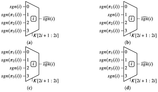
Figure 9.
Four possible configurations of the four-way multiplexer inputs depend on the obfuscation key values: (a) , where the nonpermuted sign bit is applied at input 0; (b) , where the nonpermuted sign bit is applied at input 1; (c) , where the nonpermuted sign bit is applied at input 2; and (d) , where the nonpermuted sign bit is applied at input 3.
In case of the incorrect key, is applied at the selection inputs of the four-way multiplexers; the output sign bits will represent a selection of the permuted original sign bits, which will lead to an incorrect computation of the output results. Only when the correct key, , is presented at the inputs of the four-way multiplexers, the output results computation is performed correctly. In our implementation, we have considered (base 16 representation).
3.3. VLSI Implementation
The RTL description of the IntDCT was performed using SystemVerilog. An example simulated operation of the IntDCT core implementation is illustrated in Figure 10, Figure 11 and Figure 12. The operation of the IntDCT core was exemplified for 2 batches of 16 input samples: = 121, 106, 92, 79, 67, 56, 37, 29, 22, 16, 11, 7, 4, 2, and 1, immediately followed by = 10, 20, 30, 40, 50, 60, 70, 80, 80, 70, 60, 50, 40, 30, 20, and 10.
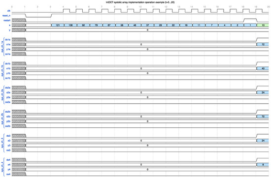
Figure 10.
Illustration of the IntDCT systolic array operation for the time unit interval. In the figure, represents the input samples to the DCT core; represents the unscaled output samples of the DCT core; and , , , , , , , , , , , and represent the inputs and outputs of the five systolic arrays corresponding to Equations (6), (7), (9)–(13), respectively. The signal resets the control state machine while the signal restarts the computations for a new input batch. The signal represents the data shift commands for the systolic arrays when input data are shifted through the chain and partial results are progressively computed. The signals are the output sample commands when valid outputs are sampled from the chains and pushed into following shift registers.
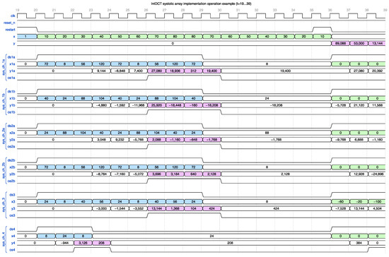
Figure 11.
Illustration of the IntDCT systolic array operation for the time unit interval. In the figure, the first input sample batch, together with the auxiliary input sequences related to this batch, are highlighted with blue, while the second input samples batch, and the corresponding auxiliary input sequences are highlighted with green. The first output samples batch is highlighted with magenta, while the second output samples batch, in the following figure, is highlighted with yellow. The partial results produced by the systolic chains are highlighted with the color corresponding to the outputs which they contribute to.
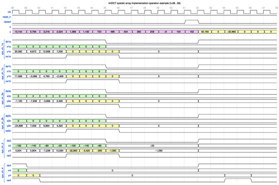
Figure 12.
Illustration of the IntDCT systolic array operation for the time unit interval.
The first output sample is produced after 32 samples, therefore the latency of the implemented IntDCT core is .
The expected unscaled output sequence for the first input batch is = 89,088, 53,000, 13,144, 5784, 3216, 2024, 1368, 1192, 720, 488, 424, 360, 208, −8, 104, and 152, which is produced by the implementation, as can be observed in Figure 10, Figure 11 and Figure 12.
In the figures, the first input sample batch is highlighted with blue and the second input samples batch is highlighted with green. The first output samples batch is highlighted with magenta and the second output samples batch is highlighted with yellow. The partial results produced by the systolic chains are highlighted with the color corresponding to the outputs which they contribute to.
For characterization purposes, we have synthesized the IntDCT core using Cadence Genus 21.14 with Nangate OpenCell Library and NCSU’s 15 nm FreePDK15. We have considered an 8 bits width for the input samples and an 18 bits width for the unscaled output samples. Table 1 summarizes the synthesis results in terms of area, power, and delay for the IntDCT. It can be observed that the minimum constrained clock period for which the synthesis tool is able to find a solution is 4.17 GHz. At this frequency, the dynamic power is 52.1 mW.

Table 1.
Summary of synthesis results of the IntDCT core.
The proposed solution has further potential for optimization by early scaling the partial results (currently, the output needs to be divided by 128, i.e., the least 7 significant bits can be discarded) along the systolic chains. Another means to increase the operating frequency is to add a pipeline stage for the computation of the auxiliary inputs in Equation (5).
4. Discussion
We have obtained a new integer algorithm for type II DCT that has good approximation properties and allows efficient VLSI implementation. Moreover, it allows an efficient integration of the obfuscation technique with low overheads. The involved overhead of incorporating the obfuscation technique is low and consists of 22 four-way, one-bit multiplexers. The area overhead of the multiplexers is under 1% of the total chip area, while the impact on the speed of the DCT core operation is minimal because the multiplexers are not on the critical data path of the systolic arrays.
For the proposed integer algorithm, a new systolic array-based VLSI architecture has been obtained. It consists of five linear arrays, each having four processing elements, and one array with two processing elements, all working in parallel. Due to the fact that the proposed integer algorithm is using only small integers and each processing element contains a multiplier with a small constant implemented with two adders (with two exceptions where we use three adders), the hardware complexity was significantly reduced and, at the same time, the speed performances were increased due to the fact that in the systolic chains the delay on the critical path is mostly , where is the delay of one adder. Thus, we can use only adders/subtracters and shift operations to implement the proposed VLSI architecture. As it can be seen from Table 2, to implement the constant multipliers we mostly need only 2 adders and shift operations, with 2 exceptions, where for coefficients 106 and 90 we use 3 adders.
Table 2.
Representation of the constant multiplication coefficients used in the PEs.
Due to the fact all five systolic arrays are working in parallel and due to the use of the pipelining mechanism, where the critical path has a delay of mostly , we can obtain high speed performances at a significantly reduced hardware cost due to the use of only adders to implement the proposed VLSI architecture. Moreover, the proposed solution can efficiently integrate the hardware security technique with a slight increase in the hardware complexity with only 22 MUXs, without affecting the speed performance.
Furthermore, the proposed solution has similar advantages to other systolic array VLSI implementations of type II DCT, such as efficient VLSI implementation and low I/O cost.
In Table 3, a comparison in terms of area, power, and speed performance is presented. The proposed IntDCT solution is compared to similar solutions from the literature.
Table 3.
Comparison of hardware performances.
All the referenced designs in Table 3 were mapped to a 45 nm standard cell library using Synopsys Design-Compiler, whereas our design was mapped to Nangate’s OpenCell Library based on NCSU’s 15 nm FreePDK15 using Cadence Genus 21.14.
As can be seen from Table 3, a considerable reduction in power consumption has been obtained for the proposed solution due to a reduced hardware complexity based on as few as 29 adders to implement the hardware core with 5 linear systolic arrays.
One of the most important advantages of using the systolic array architectural paradigm is a significant reduction in the delay on the critical path, as emphasized in Table 3, where an improvement of more than 93% was obtained as compared to the referenced designs. This has allowed for a significant increase in speed performances in our solution by using a clock frequency of up to 4.17 GHz, as illustrated in Table 1.
Another noticeable advantage of the proposed solution based on the systolic array paradigm consists of the efficient incorporation of an obfuscation technique with a small overhead.
5. Conclusions
In this paper, a new hardware algorithm for an integer based discrete cosine transform (IntDCT) was proposed that provides a good approximation of the discrete cosine transform and at the same time offers an efficient VLSI implementation using the systolic array architectural paradigm. Using a multi-objective optimization, the proposed integer transforms searches for an efficient IntDCT matrix which has the coding performance as close as possible to the DCT transform but implemented with reduced hardware/power and high-speed performances obtaining using pipelining and parallelism. The proposed integer DCT algorithm has been efficiently restructured into five regular and modular computational structures of lengths of four and one of length two called pseudo-cycle convolutions. These regular and modular computational structures allow for an efficient VLSI implementation using systolic arrays. Moreover, besides an efficient VLSI implementation with high speed, the proposed integer DCT algorithm and its VLSI architecture allow for efficient incorporation of the obfuscation technique that significantly improves the hardware security with a low overhead which maintains all the implementation performances.
Author Contributions
Conceptualization, D.F.C.; methodology, D.F.C. and A.C.; software, A.C.; validation, D.F.C. and A.C.; formal analysis, D.F.C. and A.C.; investigation, D.F.C. and A.C.; resources, D.F.C. and A.C.; writing—original draft preparation, D.F.C.; writing, review, and editing, D.F.C. and A.C.; visualization, D.F.C.; project administration, D.F.C.; funding acquisition, D.F.C. All authors have read and agreed to the published version of the manuscript.
Funding
This work was supported by a grant of the Romanian Ministry of Education and Research, CNCS—UEFISCDI, project number PCE 172/2021 (PN-III-P4-ID-PCE2020-0713), within PNCDI III.
Institutional Review Board Statement
Not applicable.
Informed Consent Statement
Not applicable.
Data Availability Statement
Not applicable.
Conflicts of Interest
The authors declare no conflict of interest.
References
- Jain, A. A Fast Karhunen-Loeve Transform for a Class of Random Processes. IEEE Trans. Commun. 1976, 24, 1023–1029. [Google Scholar] [CrossRef]
- Chan, Y.-H.; Siu, W.-C. On the Realization of Discrete Cosine Transform Using the Distributed Arithmetic. IEEE Trans. Circuits Syst. Fundam. Theory Appl. 1992, 39, 705–712. [Google Scholar] [CrossRef]
- Guo, J.-I.; Liu, C.-M.; Jen, C.-W. A New Array Architecture for Prime-Length Discrete Cosine Transform. IEEE Trans. Signal Process. 1993, 41, 436. [Google Scholar] [CrossRef]
- Meher, P.K. Systolic Designs for DCT Using a Low-Complexity Concurrent Convolutional Formulation. IEEE Trans. Circuits Syst. Video Technol. 2006, 16, 1041–1050. [Google Scholar] [CrossRef]
- Cheng, C.; Parhi, K.K. Hardware Efficient Fast DCT Based on Novel Cyclic Convolution Structures. IEEE Trans. Signal Process. 2006, 54, 4419–4434. [Google Scholar] [CrossRef]
- Chiper, D.F.; Ungureanu, P. Novel VLSI Algorithm and Architecture with Good Quantization Properties for a High-Throughput Area Efficient Systolic Array Implementation of DCT. EURASIP J. Adv. Signal Process. 2011, 2011, 639043. [Google Scholar] [CrossRef]
- Chiper, D.-F.; Cracan, A.; Burdia, D. A New Systolic Array Algorithm and Architecture for the VLSI Implementation of IDST Based on a Pseudo-Band Correlation Structure. Adv. Electr. Comput. Eng. 2017, 17, 75–80. [Google Scholar] [CrossRef]
- Kung, H.T. Why Systolic Architectures? Computer 1982, 15, 37–46. [Google Scholar] [CrossRef]
- White, S.A. Applications of Distributed Arithmetic to Digital Signal Processing: A Tutorial Review. IEEE ASSP Mag. 1989, 6, 4–19. [Google Scholar] [CrossRef]
- Sullivan, G.J. Report for 26th VCEG Meeting; ITU-T SG16/Q6 Document VCEG-Z01; ITU Telecommunication Standardization Sector: Geneva, Switzerland, 2005.
- ISO/IEC 23008-2; 2015 Information Technology—High Efficiency Coding and Media Delivery in Heterogeneous Environments—Part 2: High Efficiency Video Coding. International Organization for Standardization: Geneva, Switzerland, 2015.
- International Telecommunication Union. H.264: Advanced Video Coding for Generic Audiovisual Services; Document ITU-T Rec. H.264; International Telecommunication Union: Geneva, Switzerland, 2009. [Google Scholar]
- AVS Video Expert Group. Advanced Coding of Audio and Video—Part 2: Video; AVS Video Expert Group: Beijing, China, 2006. [Google Scholar]
- Loomis, J.; Wasson, M. VC-1 Technical Overview; Microsoft Corporation: Redmond, WA, USA, 2007. [Google Scholar]
- Sullivan, G.J.; Ohm, J.-R.; Han, W.-J.; Wiegand, T. Overview of the High Efficiency Video Coding (HEVC) Standard. IEEE Trans. Circuits Syst. Video Technol. 2012, 22, 1649–1668. [Google Scholar] [CrossRef]
- Malvar, H.S.; Hallapuro, A.; Karczewicz, M.; Kerofsky, L. Low-Complexity Transform and Quantization in H.264/AVC. IEEE Trans. Circuits Syst. Video Technol. 2003, 13, 598–603. [Google Scholar] [CrossRef]
- Wien, M. High Efficiency Video Coding: Coding Tools and Specification; Signals and Communication Technology; Springer: Berlin/Heidelberg, Germany, 2015. [Google Scholar] [CrossRef]
- Chiper, D.F.; Cracan, A. A New Integer Algorithm for a VLSI Implementation of DCT Using Obfuscation Technique. In Proceedings of the 2022 14th International Conference on Communications (COMM), Bucharest, Romania, 16–18 June 2022; pp. 1–4. [Google Scholar] [CrossRef]
- Alshina, E.; Alshin, A.; Lee, W.; Park, J.; Pachauri, K.; Topiwala, P. CE10: Full Factorization Core Transforms for HEVC; JCTVC-G737; JCT-VC: Geneva, Switzerland, 2011. [Google Scholar]
- Meher, P.K.; Park, S.Y.; Mohanty, B.K.; Lim, K.S.; Yeo, C. Efficient Integer DCT Architectures for HEVC. IEEE Trans. Circuits Syst. Video Technol. 2014, 24, 168–178. [Google Scholar] [CrossRef]
- Meher, P.K.; Lam, S.-K.; Srikanthan, T.; Kim, D.H.; Park, S.Y. Area-Time Efficient Two-Dimensional Reconfigurable Integer DCT Architecture for HEVC. Electronics 2021, 10, 603. [Google Scholar] [CrossRef]
- Zhang, J. A Practical Logic Obfuscation Technique for Hardware Security. IEEE Trans. Very Large Scale Integr. VLSI Syst. 2016, 24, 1193–1197. [Google Scholar] [CrossRef]
- Shamsi, K.; Li, M.; Meade, T.; Zhao, Z.; Pan, D.Z.; Jin, Y. AppSAT: Approximately Deobfuscating Integrated Circuits. In Proceedings of the 2017 IEEE International Symposium on Hardware Oriented Security and Trust (HOST), Mclean, VA, USA, 1–5 May 2017; pp. 95–100. [Google Scholar] [CrossRef]
- Koteshwara, S.; Kim, C.H.; Parhi, K.K. Hierarchical Functional Obfuscation of Integrated Circuits Using a Mode-Based Approach. In Proceedings of the 2017 IEEE International Symposium on Circuits and Systems (ISCAS), Baltimore, MD, USA, 28–31 May 2017; pp. 1–4. [Google Scholar] [CrossRef]
- Chen, S.; Chen, J.; Wang, L. A Chip-Level Anti-Reverse Engineering Technique. ACM J. Emerg. Technol. Comput. Syst. 2018, 14, 29:1–29:20. [Google Scholar] [CrossRef]
- Sengupta, A.; Roy, D.; Mohanty, S.P.; Corcoran, P. Low-Cost Obfuscated JPEG CODEC IP Core for Secure CE Hardware. IEEE Trans. Consum. Electron. 2018, 64, 365–374. [Google Scholar] [CrossRef]
- Koteshwara, S.; Kim, C.H.; Parhi, K.K. Key-Based Dynamic Functional Obfuscation of Integrated Circuits Using Sequentially Triggered Mode-Based Design. IEEE Trans. Inf. Forensics Secur. 2018, 13, 79–93. [Google Scholar] [CrossRef]
- Parhi, K.K.; Koteshwara, S. Dynamic Functional Obfuscation. U.S. Patent US11061997B2, 13 July 2021. Available online: https://patents.google.com/patent/US11061997B2/en (accessed on 23 March 2023).
- Chen, J.; Liu, S.; Deng, G.; Rahardja, S. Hardware Efficient Integer Discrete Cosine Transform for Efficient Image/Video Compression. IEEE Access 2019, 7, 152635–152645. [Google Scholar] [CrossRef]
- Jiang, Y.; Chen, J. A New Algorithm to Derive High Performance and Low Hardware Cost DCT for HEVC. IEEE Trans. Comput.-Aided Des. Integr. Circuits Syst. 2022, 41, 5367–5379. [Google Scholar] [CrossRef]
- Kung, S.Y. VLSI Array Processors; Prentice Hall: Hoboken, NJ, USA, 1988. [Google Scholar]
- Jen, C.-W.; Hsu, H.-Y. The Design of a Systolic Array with Tags Input. In Proceedings of the 1988 IEEE International Symposium on Circuits and Systems (ISCAS), Espoo, Finland, 7–9 June 1988; Volume 3, pp. 2263–2266. [Google Scholar] [CrossRef]
- Sun, H.; Cheng, Z.; Gharehbaghi, A.M.; Kimura, S.; Fujita, M. Approximate DCT Design for Video Encoding Based on Novel Truncation Scheme. IEEE Trans. Circuits Syst. Regul. Pap. 2019, 66, 1517–1530. [Google Scholar] [CrossRef]
- Fong, C.-K.; Han, Q.; Cham, W.-K. Recursive Integer Cosine Transform for HEVC and Future Video Coding Standards. IEEE Trans. Circuits Syst. Video Technol. 2017, 27, 326–336. [Google Scholar] [CrossRef]
Disclaimer/Publisher’s Note: The statements, opinions and data contained in all publications are solely those of the individual author(s) and contributor(s) and not of MDPI and/or the editor(s). MDPI and/or the editor(s) disclaim responsibility for any injury to people or property resulting from any ideas, methods, instructions or products referred to in the content. |
© 2023 by the authors. Licensee MDPI, Basel, Switzerland. This article is an open access article distributed under the terms and conditions of the Creative Commons Attribution (CC BY) license (https://creativecommons.org/licenses/by/4.0/).