Abstract
A shortwave infrared Ge–Si photodetector will become the core device of the LiDAR optical receiver. In order to meet the urgent demand for photodetectors in the LiDAR field, we designed and produced a 32 × 32-pixel Ge–Si photodetector array, which was proposed and developed to meet the performance requirements of the detector array. A dark current detection system for fast scanning and detecting large-scale Ge–Si detector arrays was proposed and developed to achieve the rapid detection of dark current in each detector pixel, with a detection accuracy of less than 1 nA. The system validated the primary performance indicators of the detector array we designed, achieving rapid discrimination of the array performance and rapid localization of damaged pixels. The scanning test results showed that the average dark current of the designed detector array chip was on the nanoampere level, and the proportion of bad points was less than 1%. The consistency of the array chip was high, which meets the requirements of light detection at the receiving end of LiDAR. This work laid the foundation for our subsequent development of a LiDAR prototype system.
1. Introduction
The application of LiDAR is extensive, and in the future, it will have a large market worth hundreds of billions of yuan [1,2,3]. LiDAR is a radar system that uses lasers to accurately measure the position, velocity, and other characteristics of targets. It is an optical remote-sensing technology that can transmit distance information from the real world to computers, giving machines human depth vision and providing the function of “eyes” for humans to explore a wider three-dimensional world. LiDAR can be used for intelligent transportation, the real-time monitoring of vehicle characteristics (size, speed, and volume), and flow; intelligent vehicle (intelligent connected vehicles) ranging and speed measurements and obstacle avoidance navigation; intelligent robots to achieve precise positioning, gesture recognition, etc.; unmanned aerial vehicles for land surveying and environmental monitoring; intelligent healthcare, by achieving virtual imaging and 3D printing; and digital cities, urban 3D modeling, digital maps, etc. [4,5,6,7,8,9]. In the military, it can be used for battlefield reconnaissance, fighter telemetry, fire control tracking, underwater detection, laser communication, electronic countermeasures, and so on [10,11,12,13]. Shortwave infrared is safer for the human eye and is the best choice for LiDAR light sources. Shortwave infrared generally refers to wavelengths of 0.9~1.7 μm [14]. Electromagnetic waves between 0.9 μm and 1.7 μm cannot be seen by the human eye, but they are very similar to visible light and can be reflected on the surface of an object. The image has shadows and contrast, making the object easy to recognize. Shortwave infrared technology has a series of outstanding advantages such as high recognition, all-weather adaptation, low-light night vision, covert active imaging, and simple optical configuration, giving it special application prospects in fields such as aerospace remote sensing, archaeological identification, military reconnaissance, public safety, industrial testing, medical diagnoses, etc. [15,16,17].
Although MoO3-based ultraviolet photodetectors have an extremely high responsiveness, their operating wavelengths are usually 300–400 nm [18]. However, for automotive LiDAR applications, eye-safe shortwave infrared LiDAR will be the mainstream direction in the future. Presently, short-infrared-wavelength InGaAs avalanche photodiode detectors are starting to be applied in high-end LiDAR, but the cost is relatively high [19]. For example, the 32 × 1-linear-array InGaAs detector array produced by Hamamatsu Photonics in Japan has a dark current of less than 2.5 nA and a response of 0.95 A/W, which belongs to the more advanced InGaAs detector array at present. However, the unit price of the three-line array is as high as USD 1000 [20]. Ge–Si photodetectors compatible with CMOS technology with lower costs have been extensively studied in the past decade and remarkable progress has been made [21,22,23,24,25,26,27,28,29,30]. Especially in the past couple of years, at low temperatures, research has shown that the performance of Ge avalanche photodiode single-photon detectors is comparable to that of InGaAs [21]. Moreover, from an integration perspective, making Ge photodetectors on single-crystal Si is compatible with Si-based CMOS technology and can be integrated with optical circuits on a single chip. With a low cost and high integration, it will become the mainstream for LiDAR detectors. Therefore, the research on Ge–Si photodetectors has become increasingly important. Early Ge–Si photodetectors were mainly used in the field of optical communication, so more attention was paid to the gain–bandwidth product and the weak light detection limit. The gain–bandwidth product reached above 300 GHz [22,23]. The Si waveguide made by the Institute of Electronics at the Université Paris-Sud on a 300 nm Ge epitaxial layer was integrated with a Ge–Si photodetector on a single chip. The weak light detection limit could be as low as −35 dBm, while the bias voltage was only 7 V [24]. The University of Heriot–Watt in the UK conducted research on single-photon Ge–Si APDs (avalanche photodiodes). In 2013, they produced a traditional vertical-structure Ge–Si APD, which achieved a single-photon detection function in the Geiger mode at the low temperature of 100 K [25]. The Sandia National Laboratory in the United States produced a novel horizontal-structure Ge–Si APD, which improved the single-photon detection efficiency to 5.27%, providing a solid technical foundation for implementing ultra-long-range LiDAR [26]. The Singapore Institute of Microelectronics first reported the research results of Ge–Si APD arrays forming photomultiplier tubes at the 2019 OFC International Conference [27], and the photoelectric detection efficiency between array units showed good consistency. However, the dark current was still relatively high, and the dark current near the breakdown voltage of the single-transistor APD also reached the μA level. Academician Wang Qiming’s research group at the Institute of Semiconductors of the Chinese Academy of Sciences studied the epitaxial growth of Ge on monocrystalline silicon using ultra-high-vacuum CVD (chemical vapor deposition). Recently, extensive research has been conducted on Ge–Sn alloys [28]. Xiamen University studied upper and lower DBR (distributed Bragg reflector) microcavity-enhanced germanium photodetectors with similar surface emission structures [29], but the photoelectric conversion efficiency was slightly low. The Zhiping Zhou research group at Peking University studied a short-cavity Ge–Si photodetector with an enhanced horizontal DBR reflection of 5 μm. The long absorption region achieved a photoelectric conversion efficiency of 0.72 A/W, the 3 dB bandwidth reached 31.7 GHz, and the dark current was only 7 nA [30].
In response to the urgent demand for photodetectors in the field of LiDAR, we conducted research on PIN-type Ge–Si photodetectors. By optimizing the doping structure and concentration design, we effectively suppressed the electric field distributed at Ge and Si heterojunctions and prepared a low-dark-current and high-responsiveness 32 × 32-pixel Ge–Si photodetector array. In order to test the performance of the detector array, we needed to design a fast dark current detection system. The system quickly scans each pixel of the array, applies different bias voltages to each pixel, and reads the different dark currents generated by the pixel. The photocurrent generated by the detector includes the sum of the photogenerated current and the dark current. If the proportion of dark current is large, the photocurrent cannot effectively characterize the photoelectric conversion performance of the detector, and the dark current of the detector is inversely proportional to its optical response characteristics.
Usually, the dark current of photodetectors is at the nanoampere level and has a large range of variation. It is generally necessary to use high-gain preamplifier circuits and a range of automatic conversion circuits to achieve this [31,32,33]. For detector arrays, it is necessary to design corresponding scanning circuits to select pixels [34], similar to the imaging principle of charge-coupled device (CCD) cameras. Based on the characteristics of Ge–Si detector arrays and the design principles of detection circuits, our detection system can quickly detect the dark current distribution of the entire array and locate damaged pixels, providing us with testing and verification methods for device design. It can be used for the rapid detection of dark currents in larger detector arrays in the future.
2. Principle and System
2.1. New Ge–Si Detector Array
A photodetector is a device that converts light signals into electrical signals. In order to effectively capture the reflected light signals of the target object on the LiDAR in space, we designed and prepared a 32 × 32-pixel Ge–Si photodetector array with a Ge active area of up to 707 μm2, as shown in Figure 1. The array consisted of pixels, leads, and electrodes. The pixel-doping structure was achieved by injecting boron elements into the top Si layer on the SOI wafer, forming a P-type doping region and a heavily doped P++ region, respectively. The P++ region formed a cathode through ohmic contact with the Al metal electrode. Afterward, selective epitaxy was carried out on the Si substrate to prepare Ge thin films as the active absorption region of the detector. Finally, phosphorus was injected above the Ge absorption region to form a heavily doped N++ region, which formed an anode through ohmic contact with the Al electrode.
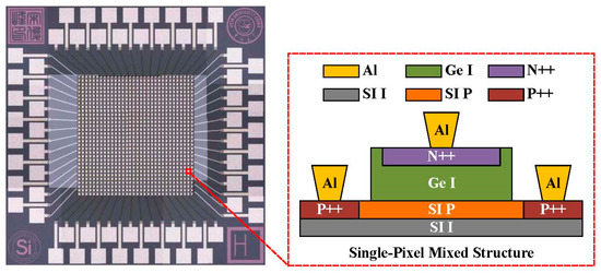
Figure 1.
New Ge–Si detector array structure.
In order to characterize the photodetectors, we mainly studied their responsivity and quantum efficiency, dark current, noise characteristics, response bandwidth, gain, gain–bandwidth product, and other parameters [35]. When the photodetector is in a reverse-bias state, even without incident light, a weak current is generated, which is known as a dark current. Dark current generation is related to the electron–hole pairs generated by the thermal motion inside the detector. On the other hand, it is related to the defect of the detector surface, bias voltage, and surface area. Figure 2a shows the equivalent circuit model of the PIN photodetector under no light conditions. In the circuit, Cj is the junction capacitance, Cs is the equivalent parallel capacitance, Rs is the equivalent series resistance, and the dark current Idark includes the reverse-bias current Igen, the tunneling current Itun, and the parasitic leakage current Iohm [36]. In addition, the dark current is related to the thermal ion emission and temperature [18], and its impact on Ge–Si detectors is relatively small and can be ignored. Figure 2b shows the corresponding bias voltage–dark current curve, where the dark current increases with an increase in the reverse-bias voltage.
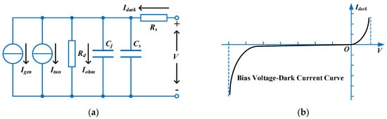
Figure 2.
PIN photodetector circuit model and dark current curve. (a) PIN-equivalent circuit model under no illumination. (b) Bias voltage–dark current curve.
As shown in Equation (1), the dark current can be expressed as:
Under reverse-bias voltage, electron–hole pairs are generated in the space charge region. Once an electron hole is generated, it is swept out of the space charge region by an electric field, forming a reverse bias to generate current. Equation (2) is the calculation method for the current Igen generated by reverse bias:
where τ0 is the average lifetime of the carrier, ni is the intrinsic carrier concentration, e is the electron charge, w is the volume of the space charge region, and A is the device area.
According to the tunneling effect, when the reverse-bias voltage is too high, the probability of carriers passing through the barrier width of the space charge region greatly increases, resulting in a large current that cannot be ignored. This current is called the tunneling current, and the calculation method for the tunneling current is:
where E is the maximum field strength in the depletion region of the PN junction, V is the applied reverse-bias voltage, A is the device area, m* is the effective mass of the electron, Eg is the energy band gap, ħ is the reduced Planck constant, and e is the electronic quantity.
The expression for the parasitic leakage current is:
where V is the bias voltage applied at both ends of the detector and Rd is the dark resistance of the photodetector. Generally, the dark current mainly generates current and parasitic leakage current at a low bias and tunneling current at a high bias. Therefore, it is necessary to check the distribution of dark current under different reverse-bias voltages and improve the photodetector performance; efforts should be made to reduce dark current.
2.2. Scanning Detection Method and System
Figure 3 is the principal block diagram of the Ge–Si-detector-array dark-current fast detection system, which consists of a controllable voltage source, a Ge–Si detector array and its scanning circuit, an electrometer-level amplifier, a programmable amplifier, an MCU (micro-controller), and an LCD (liquid crystal display). During the working process, the MCU controls the bipolar DAC (digital-to-analog converter) output voltage in the controllable voltage source, which is amplified by a voltage follower to generate a controllable bias voltage. The controllable bias voltage is loaded onto the optical relay. The MCU controls the 3–8 decoder for row selection, selecting one row of pixels to make one row of pixels conductive. The MCU also controls the 3–8 decoder for column selection, selecting one column of pixels to make one column of pixels conductive. Finally, the bias voltage is applied to a single detector. The dark current signal generated by the pixel generates a voltage signal through the electrometer amplifier. The generated voltage signal is amplified by the programmable amplifier. The amplified voltage signal is input to the ADC (analog-to-digital converter) module in the MCU and converted into a digital signal displayed on the LCD screen. This system can achieve rapid scanning and dark current detection of large-scale Ge–Si detector arrays.
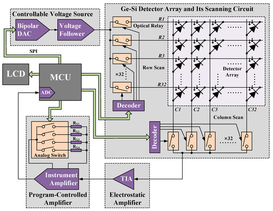
Figure 3.
Schematic diagram of the composition of the detection system.
The controllable voltage source consists of a bipolar DAC and a voltage follower, with a bipolar DAC power supply voltage of ±5 V. Therefore, the bias voltage range of the detector can reach −5 V to +5 V. We continuously read the dark current under reverse-bias voltage and positive-bias voltage. The actual voltage scanning range was −3 V~+1 V. As shown in Figure 4, the bipolar DAC chip used ADI (Analog Devices Inc.)’s LTC2664-12. The DAC chip had four output channels, one of which was used for actual measurement. If the DAC is 12 bits, the voltage resolution is:
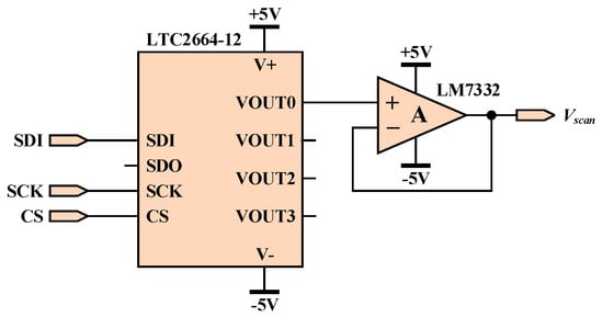
Figure 4.
Schematic diagram of controllable voltage source circuit.
The voltage follower was implemented using Texas Instrument’s high-output current amplifier LM7332, which can output a maximum current of up to 70 mA.
The dark current amplification circuit is shown in Figure 5, consisting of a cross-impedance amplifier (TIA), a programmable amplifier, and a general-purpose amplifier. The TIA was realized by an electrometer amplifier ADA4530-1 of ADI. This chip is an operational amplifier with an input bias current on a flying ampere level, which is suitable for measuring weak currents. The impedance connected in Figure 5 was 1 MΩ, so the output voltage of the TIA is:
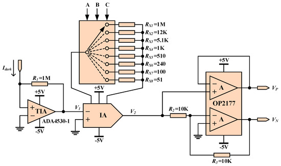
Figure 5.
Dark current amplification circuit.
Due to the extensive dark current variations in PD detectors, especially in the case of reverse bias and forward bias, there is a greater difference in the current. Therefore, a programmable amplifier was used to amplify V1 to ensure a variable amplification factor. The programmable amplifier consisted of ADI’s instrument amplifier AD8220 and a single-pole 8-position analog switch. The amplification factor of AD8220 is:
The eight resistors connected to the single-pole 8-position analog switch were 1 MΩ, 12 KΩ, 5.1 KΩ, 1 KΩ, 510 Ω, 240 Ω, 100 Ω, and 51 Ω. Based on the resistors Rx1~Rx8, the corresponding amplification factors can be calculated as 1.05, 5.22, 9.36, 50.40, 97.86, 206.83, 495.00, and 969.63. During testing, adjusting the amplification factor according to the size of the measured value can improve the measurement accuracy, with A, B, and C being the address inputs of the analog switch controlled by the MCU.
Due to the negative dark current of the PD detector under reverse bias and the positive dark current under forward bias, V2 can be either positive or negative, while the ADC inside the MCU can only read positive voltages. Therefore, we designed a third-stage amplification circuit, which outputs in-phase voltages on one side and reverses voltages on the other side; namely:
when Idark < 0, VP > 0, and VN < 0, the ADC reads the voltage of VP. When Idark > 0, VP < 0, and VN > 0, the ADC reads the voltage of VN. We used two ADC channels to read the Idark for reverse and forward bias.
Using the Toshiba semiconductor’s optical relay TLP3320 to achieve the row and column selection of detector arrays and to replace mechanical relays with optical relays can reduce the installation area and achieve fast switch selection. Figure 6a shows the internal structure of an optical relay, which is similar in principle to an optocoupler. The switching speed of TLP3320 is less than 300 μs. This system can achieve fast scanning of the array. The on-resistance of TLP3320 is about 10 Ω, and the off-resistance is about 1014 Ω. Usually, the dark current of the PD detector is between 1 and 100 nA under a reverse-bias voltage of 1 V, and the equivalent resistance of PD is between 107 and 109 Ω. If the on-resistance RON of TLP3320 is set to 10 Ω, the off-resistance ROFF is set to 1014 Ω, and the equivalent resistance RPD of PD is set to 108 Ω, then the equivalent circuit of the array is that shown in Figure 6b. The on-current ION is approximately 1013 times the off-current IOFF, so the influence of the off-resistance can be ignored. The dark current IA on the PD detector in the first row and column selected in Figure 6b is approximately equal to the dark current Idark of the array.
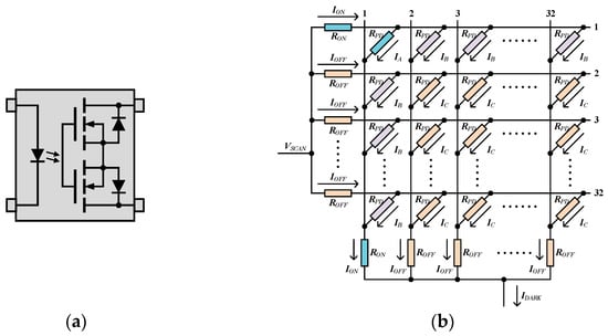
Figure 6.
Optical relays and their equivalent circuits. (a) Internal structure of optical relays. (b) Equivalent scanning circuit.
As shown in Figure 7, the hardware diagram of the detection system is composed of a Ge–Si detector array and its scanning circuit, a variable voltage source, a dark current detection circuit, a control circuit, and an LCD screen. The Ge–Si detector array is placed in the middle of the scanning circuit, and pixel selection is carried out by an optical relay. The variable voltage source and dark current detection circuit are integrated on a printed circuit board (PCB), and the bias voltage is output to the scanning circuit. The dark current is also connected to the dark current detection circuit from the scanning circuit. The control circuit is located below the LCD screen, and the MCU used is the ARM chip STM32F103ZET6 from STMicroelectronics. The LCD screen can draw a bias voltage–dark current curve and display the magnitude of dark current under different bias voltages. The system detection includes two modules: single measurement and continuous measurement. In the single-measurement mode, rows and columns can be selected, and the bias voltage–dark current curve of the row and column pixels can be measured in a single measurement. By continuously measuring the modulus, we can automatically measure the bias voltage–dark current curve of all pixels at once and ultimately store all test data in the SD (secure digital memory) card. By inserting the SD card into the computer host, we can read all the data.
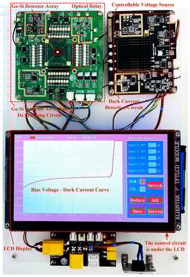
Figure 7.
Hardware physical diagram of the detection system.
3. Array Test and Data Analysis
We designed detector arrays of four different sizes, A, B, C, and D. The target surface of array A is 2.5 cm × 2.5 cm, that of array B is 2.0 cm × 2.0 cm, that of array C is 1.5 cm × 1.5 cm, and that of array D is 1.0 cm × 1.0 cm, as shown in Figure 8. The photosensitive surface of a pixel accounts for about half of the whole pixel area, that is, the fill factor of all devices is 0.5. We needed to detect dark current on these four arrays and determine the distribution of dark current and pixel consistency under different sizes, ultimately guiding us in device design.
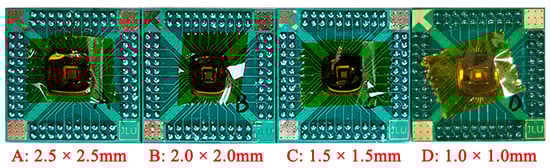
Figure 8.
PD array chips (A–D).
Firstly, we measured a single pixel’s bias voltage–dark current curve, as shown in Figure 9. The voltage scanning range was −3500 mV~+100 mV, and the step voltage was 50 mV. As shown in Figure 9, the bias voltage–dark current curve of the first-row and first-column pixels of device A was consistent with the theoretical curve in Figure 2.
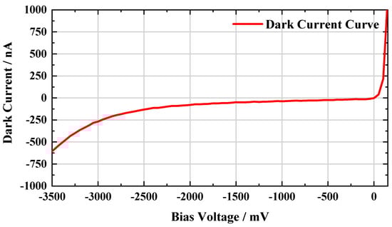
Figure 9.
The bias voltage–dark current curve of the pixel (the first-row and first-column pixels of device A).
Furthermore, we measured all dark currents in the device and determined their distribution characteristics. Figure 10 shows the two-dimensional histogram of the dark current distribution of device A, and Figure 10 shows the two-dimensional histogram of the dark current distribution at the bias voltages −2.5 V, −2.0 V, −1.5 V, −1.0 V, and −0.5 V. The higher part of the histogram in the figure shows a large and abnormal dark current. To quantify the array damage, we counted the number of pixels > 10 times the average dark current and the number of pixels > five times the average dark current. Table 1 shows the measurement results. The number of pixels with device A > 10 times the average dark current was two, totaling 1024 pixels and accounting for 0.2%. The number of pixels with device A > five times the average dark current was nine, accounting for 0.9%. The pixel damage of device A was <1%, indicating a good performance. Our system can continuously detect device damage and quickly locate the position of damaged pixels, so we can respond to imaging applications through compensation in the later stage.
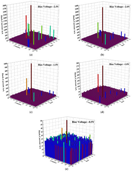
Figure 10.
Histogram distribution of dark current test for PD array A. (a) Bias voltage = −2.5 V. (b) Bias voltage = −2.0 V. (c) Bias voltage = −1.5 V. (d) Bias voltage = −1.0 V. (e) Bias voltage = −0.5 V.

Table 1.
PD array A’s dark current parameters.
Further, we measured the dark current and its distribution of devices A, B, C, and D, as shown in Table 2. According to the theoretical design, the smaller the pixel area, the smaller the average dark current. Figure 11a shows the average dark current values of devices A, B, C, and D when the bias voltages were −2.5 V, −2.0 V, −1.5 V, −1.0 V, and −0.5 V. The higher the reverse-bias voltage, the larger the average dark current. In theory, the average dark current is in the order A > B > C > D. In actual measurements, A > B > C ≈ D was shown, and the pixel areas of devices C and D were not significantly different. All average dark currents were indistinguishable. The actual measurement was consistent with the theoretical analysis.
Table 2.
Distribution characteristics of dark current in PD arrays A, B, C, and D.
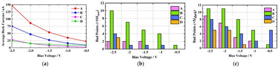
Figure 11.
Distribution of dark currents in PD arrays A, B, C, and D. (a) Average dark current distribution. (b) Distribution of the number of pixels > 10 times the average dark current. (c) Distribution of the number of pixels > 5 times the average dark current.
Figure 11b,c show the number of pixels with a bias voltage of −2.5 V, −2.0 V, −1.5 V, −1.0 V, and −0.5 V for devices A, B, C, and D > 10 times the average dark current and five times the average dark current, respectively. All devices had a pixel damage rate < 1%, indicating a good performance. Among them, device B had the most severe pixel damage and the worst performance, while device D had the least pixel damage and the best performance. The damage to devices A and C was relatively small and basically equivalent, and both had a good performance. The above measurement results can guide us in the design of Ge–Si detector array chips. The detection system has a good performance and can quickly detect the dark current characteristics of the device.
By further studying the device’s performance and verifying the functionality of the testing system, we measured the detector array’s photocurrent to obtain the array chip’s average response. We used a laser wavelength of 1550 nm with a power of −6.78 dBm and irradiated it on the detector array chip. The responses of devices A, B, C, and D are shown in Table 3. In addition, Figure 12 also shows plotted histograms of the response of these four devices. Device A had the highest responsiveness, followed by B, C, and D. Device A had the largest effective photosensitive area and the best effect. The average response of device A was greater than 0.4 A/W, which was about half of the response of the InGaAs detector of Hamamatsu Photonics at 0.95 A/W, indicating a better performance.
Table 3.
Responsiveness of devices A, B, C, and D under different bias voltages.
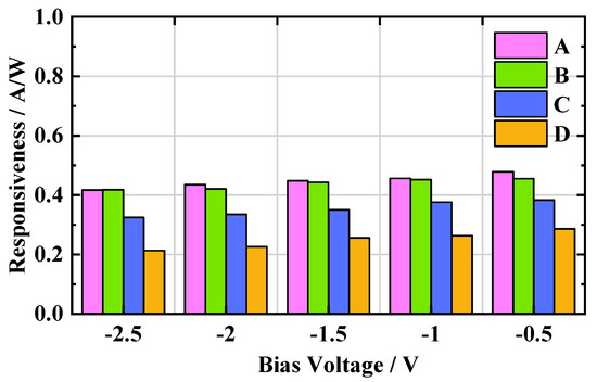
Figure 12.
Responsiveness of devices A, B, C, and D under different bias voltages.
4. Conclusions
By analyzing the dark current characteristics and detection methods of Ge–Si photodetector arrays, this paper proposed and developed a dark current detection system for the rapid scanning and detection of large-scale Ge–Si detector arrays. The high-isolation optical relay was used to quickly select the pixels of the array chip, and the electrometer amplifier was used to amplify the dark current to quickly detect the dark current of each pixel of the detector. We used this system to detect dark currents on array devices. The experimental results indicate that our designed system achieved rapid discrimination of the array performance and rapid localization of damaged pixels. The scanning test results show that the average dark current of the detector array chip was on the nanoampere level, and the proportion of bad points was <1%. The consistency of the array chip was high, which meets the requirements of light detection at the receiving end of LiDAR. This work laid the foundation for our subsequent development of a LiDAR prototype system.
Author Contributions
Methodology, Z.G.; software, Z.G.; validation, X.L.; formal analysis, Z.L.; investigation, Z.W.; resources, C.L.; data curation, J.S.; writing—original draft preparation, Z.G.; writing—review and editing, M.T.; supervision, J.S.; project administration, M.T.; funding acquisition, J.S. All authors have read and agreed to the published version of the manuscript.
Funding
This research was funded by the National Natural Science Foundation of China, grant numbers 62090053, 62090054, and 61934003; the Major Scientific and Technological Program of Jilin Province, grant number 20200501007GX; the Project of Industrial Technology Research and Development of Jilin Provincial Development and Reform Commission, grant number 2020C019-2; and the Program for JLU Science and Technology Innovative Research Team, grant number 2021TD-39.
Institutional Review Board Statement
Not applicable.
Informed Consent Statement
Not applicable.
Data Availability Statement
The raw/processed data required to reproduce these findings cannot be shared at this time, as they are part of an ongoing study.
Acknowledgments
We are grateful to the anonymous reviewers for constructive comments that improved the quality of the work.
Conflicts of Interest
The authors declare no conflict of interest.
References
- Yang, F. Analysis of Lidar Technology Development Based on Autonomous Driving Competition. In Proceedings of the International Conference of Optical Imaging and Measurement (ICOIM), Xi’an, China, 27–29 August 2021. [Google Scholar]
- Roriz, R.; Cabral, J.; Gomes, T. Automotive LiDAR Technology: A Survey. IEEE Trans. Intell. Transp. Syst. 2022, 23, 6282–6297. [Google Scholar] [CrossRef]
- Zhaohua, L.; Bochao, G. Radar Sensors in Automatic Driving Cars. In Proceedings of the International Conference on Electromechanical Control Technology and Transportation (ICECTT), Nanchang, China, 15–17 May 2020. [Google Scholar]
- Shan, Y.; Yao, X.; Lin, H.; Zou, X.; Huang, K. Lidar-Based Stable Navigable Region Detection for Unmanned Surface Vehicles. IEEE Trans. Instrum. Meas. 2021, 70, 8501613. [Google Scholar] [CrossRef]
- Chiang, K.W.; Tsai, G.J.; Li, Y.H.; El-Sheimy, N. Development of LiDAR-Based UAV System for Environment Reconstruction. IEEE Geosci. Remote Sens. Lett. 2017, 14, 1790–1794. [Google Scholar] [CrossRef]
- Molebny, V.; McManamon, P.; Steinvall, O.; Kobayashi, T.; Chen, W. Laser radar: Historical prospective—From the East to the West. Opt. Eng. 2016, 56, 031220. [Google Scholar] [CrossRef]
- Månefjord, H.; Müller, L.; Li, M.; Salvador, J.; Blomqvist, S.; Runemark, A.; Kirkeby, C.; Ignell, R.; Bood, J.; Brydegaard, M.; et al. 3D-Printed Fluorescence Hyperspectral Lidar for Monitoring Tagged Insects. IEEE J. Sel. Top. Quantum Electron. 2022, 28, 7100109. [Google Scholar] [CrossRef]
- Sanjaya, K.; Henning, F.; Purba, K.R. 3D LIDAR City Model Application and Marketing Plan Development. In Proceedings of the International Conference on Soft Computing, Intelligent System and Information Technology (ICSIIT), Denpasar, Indonesia, 26–29 September 2017. [Google Scholar]
- Mongus, D.; Žalik, B. Computationally Efficient Method for the Generation of a Digital Terrain Model from Airborne LiDAR Data Using Connected Operators. IEEE J. Sel. Top. Appl. Earth Obs. Remote Sens. 2014, 7, 340–351. [Google Scholar] [CrossRef]
- Dai, J.; Zhao, X.; Li, L.P.; Ma, X.F. GCD-YOLOv5: An Armored Target Recognition Algorithm in Complex Environments Based on Array Lidar. IEEE Photonics J. 2022, 14, 3937711. [Google Scholar] [CrossRef]
- Singh, L.; Srivastava, A.; Sarkate, A.J. Thermal gradient effect on focus shift of laser & infrared optical assembly & thermal lensing by Nd-Yag laser rod in laser assembly of Optical Detection & Ranging System of Fighter Aircraft. In Proceedings of the IEEE Uttar Pradesh Section International Conference on Electrical, Computer and Electronics (UPCON), Mathura, India, 26–28 October 2017. [Google Scholar]
- Zhou, G.; Li, C.; Zhang, D.; Liu, D.; Zhou, X.; Zhan, J. Overview of Underwater Transmission Characteristics of Oceanic LiDAR. IEEE J. Sel. Top. Appl. Earth Obs. Remote Sens. 2021, 14, 8144–8159. [Google Scholar] [CrossRef]
- Hecht, J. Laser instruments earn their place in space for communications and lidar. Laser Focus World Mag. Photonics Optoelectron. Ind. 2014, 50, 27–31. [Google Scholar]
- Pham, T.; Du, W.; Tran, H.; Margetis, J.; Tolle, J.; Sun, G.; Soref, R.A.; Naseem, H.A.; Li, B.; Yu, S.Q. Systematic study of Si-based GeSn photodiodes with 26m detector cutoff for short-wave infrared detection. Opt. Express 2016, 24, 4519. [Google Scholar] [CrossRef]
- Batshev, V.I.; Boritko, S.V.; Kozlov, A.B.; Sharikova, M.O.; Lomonov, V.A. Optical System of Visible and Short-Wave Infrared AOTF-based Spectral Imaging Device. In Proceedings of the Wave Electronics and its Application in Information and Telecommunication Systems (WECONF), St. Petersburg, Russia, 31 May–4 June 2021. [Google Scholar]
- Xu, M.; Wang, J.L.; Chen, T. Study on application of short wave infrared to detecting satellites in the daytime. Opt. Technol. 2008, 34, 277–280. [Google Scholar]
- Qi, J.; Sun, C.; Zebibula, A.; Zhang, H.; Kwok, R.T.; Zhao, X.; Xi, W.; Lam, J.W.Y.; Qian, J.; Tang, B.Z. Real-Time and High-Resolution Bioimaging with Bright Aggregation-Induced Emission Dots in Short-Wave Infrared Region. Adv. Mater. 2018, 30, 1706856. [Google Scholar] [CrossRef]
- Basyooni, M.A.; Gaballah, A.E.H.; Tihtih, M.; Derkaoui, I.; Zaki, S.E.; Eker, Y.R.; Ateş, Ş. Thermionic Emission of Atomic Layer Deposited MoO3/Si UV Photodetectors. Materials 2023, 16, 2766. [Google Scholar] [CrossRef]
- Millar, R.W.; Kirdoda, J.; Kuzmenko, K.; Vines, P.; Halimi, A.; Collins, R.J.; Maccarone, A.; McCarthy, A.; Greener, Z.M.; Thorburn, F.; et al. Ge-on-Si Single Photon Avalanche Diode Detectors for LIDAR in the Short Wave Infrared. In Proceedings of the Conference on Lasers and Electro-Optics (CLEO), San Jose, CA, USA, 10–15 May 2020. [Google Scholar]
- Hamamatsu Photonics Co., Ltd. InGaAs PIN Photodiode Arrays G12430 Series; Hamamatsu Photonics Co., Ltd.: Hamamatsu City, Japan, 2017. [Google Scholar]
- Vines, P.; Kuzmenko, K.; Kirdoda, J.; Dumas, D.C.; Mirza, M.M.; Millar, R.W.; Paul, D.J.; Buller, G.S. High performance planar germanium-on-silicon single-photon avalanche diode detectors. Nat. Commun. 2019, 10, 1086. [Google Scholar] [CrossRef]
- Duan, N.; Liow, T.Y.; Lim AE, J.; Ding, L.; Lo, G. 310 GHz gain-bandwidth product Ge/Si avalanche photodetector for 1550 nm light detection. Opt. Express 2012, 20, 11031. [Google Scholar] [CrossRef]
- Kang, Y.; Liu, H.D.; Morse, M.; Paniccia, M.J.; Zadka, M.; Litski, S.; Sarid, G.; Pauchard, A.; Kuo, Y.H.; Chen, H.W.; et al. Monolithic germanium/silicon avalanche photodiodes with 340 GHz gain–bandwidth product. Nat. Photonics 2009, 3, 59–63. [Google Scholar] [CrossRef]
- Virot, L.; Crozat, P.; Fédéli, J.M.; Hartmann, J.M.; Marris-Morini, D.; Cassan, E.; Boeuf, F.; Vivien, L. Germanium avalanche receiver for low power interconnects. Nat. Commun. 2014, 5, 4957. [Google Scholar] [CrossRef] [PubMed]
- Warburton, R.E.; Intermite, G.; Myronov, M.; Allred, P.; Leadley, D.R.; Gallacher, K.; Paul, D.J.; Pilgrim, N.J.; Lever, L.J.M.; Ikonic, Z.; et al. Ge-on-Si Single-Photon Avalanche Diode Detectors: Design, Modeling, Fabrication, and Characterization at Wavelengths 1310 and 1550 nm. IEEE Trans. Electron Devices 2013, 60, 3807–3813. [Google Scholar] [CrossRef]
- Martinez, N.J.; Gehl, M.; Derose, C.T.; Starbuck, A.L.; Pomerene, A.T.; Lentine, A.L.; Trotter, D.C.; Davids, P.S. Single photon detection in a waveguide-coupled Ge-on-Si lateral avalanche photodiode. Opt. Express 2017, 25, 16130–16139. [Google Scholar] [CrossRef]
- Li, Y.; Luo, X.-S.; Liang, G.; Lo, G.Q. Demonstration of Ge/Si Avalanche Photodetector Arrays for Lidar Application; Optica Publishing Group: Washington, DC, USA, 2019. [Google Scholar]
- Zhang, D.L.; Cheng, B.W.; Xue, C.L.; Zhang, X.; Cong, H.; Liu, Z.; Zhang, G.Z.; Wang, Q.M. Theoretical study of the optical gain characteristics of a Ge1xSnx alloy for a short-wave infrared laser. Chin. Phys. B 2015, 7, 024211. [Google Scholar] [CrossRef]
- Zhimeng, C.; Liqun, C.; Cheng, L. Characteristics of SOI-Based RCE-Ge photodetectors. J. Fuzhou Univ. 2016, 44, 656. [Google Scholar]
- Cui, J.; Zhou, Z. High-performance Ge-on-Si photodetector with optimized DBR location. Opt. Lett. 2017, 42, 5141–5144. [Google Scholar] [CrossRef]
- Xu, S.; Deng, Z.; Xu, H.; Feng, J. Design of preamplifier and range automatic switching circuit using in light intensity detection. Electron. Des. Eng. 2015, 23, 99–104. [Google Scholar]
- De Marcellis, A.; Palange, E.; Leone, S.; Stanchieri, G.D.P.; Faccio, M. Photodiode Bridge-Based Differential Readout Circuit for High-Sensitivity Measurements of Energy Variations of Laser Pulses for Optoelectronic Sensing Systems. In Proceedings of the 2018 New Generation of CAS (NGCAS), Valletta, Malta, 20–23 November 2018. [Google Scholar]
- Pallares, J.; Cabre, R.; Marsal, L.F.; Schropp, R.E.I. A compact equivalent circuit for the dark current-voltage characteristics of nonideal solar cells. J. Appl. Phys. 2006, 100, 465. [Google Scholar] [CrossRef]
- Hwang, Y.S.; Wang, S.C.; Lai, B.P.; Chen, J.J. Controllable readout circuit for indium gallium arsenide photodiode array applications. IET Circuits Devices Syst. 2009, 3, 125–134. [Google Scholar] [CrossRef]
- Zhang, H.; Ke, C.; Liu, Z. Modeling and simulation analysis of PIN photodetector. J. Appl. Opt. 2019, 40, 723–730. [Google Scholar]
- Zhao, J. Research on Photodetector Equivalent Circuit Model and Experiment; Chongqing University: Chongqing, China, 2015. [Google Scholar]


Disclaimer/Publisher’s Note: The statements, opinions and data contained in all publications are solely those of the individual author(s) and contributor(s) and not of MDPI and/or the editor(s). MDPI and/or the editor(s) disclaim responsibility for any injury to people or property resulting from any ideas, methods, instructions or products referred to in the content. |
© 2023 by the authors. Licensee MDPI, Basel, Switzerland. This article is an open access article distributed under the terms and conditions of the Creative Commons Attribution (CC BY) license (https://creativecommons.org/licenses/by/4.0/).