Abstract
This paper describes a 2.4-GHz fully-integrated front-end receiver including a single-pole triple-throw (SP3T) switch and a low-noise amplifier (LNA) with bypass function, which was fabricated in a 0.25 μm GaAs pHEMT process. An asymmetrical SP3T switch architecture is incorporated to enable the receiver to operate in four modes. The exploration of impedance and voltage gain behavior of the proposed LNA help to establish the matching network and alleviate the trade-off between noise figure (NF) and gain performance. In LNA high gain mode, the implemented front-end receiver shows 1.7 dB of NF and 6dBm of input third-order intercept point (IIP3) with 20 dB of power gain drawing 11 mA of current from 5 V power supply at 2.4 GHz. All input and output return loss had exceeded 10 dB with fully on-chip impedance matching network. In bypass mode, the measured insertion loss of typically 7.5 dB is achieved.
1. Introduction
The requirements of high-quality and low-cost wireless local area network (WLAN) applications cause strong efforts for the development of radio frequency (RF) front-end modules (FEMs). As an essential part of the RF FEM, the receiver low-noise amplifier (LNA) generally integrates a single-pole double-throw (SPDT) switch for transmitting and receiving paths because the WLAN standards are time division duplex (TDD) communication systems [1,2]. Furthermore, to emerge short-range wireless communication markets, such as WLAN and Bluetooth, the feasibility of integrating a single-pole triple-throw (SP3T) switch into a front-end receiver has been pointed out for the 2.4–2.5 GHz frequency range [3,4].
Among various process technologies, silicon-based CMOS processes are desirable for the WLAN front-end receiver due to their lower cost and better integration capability. The study in [5] shows that an LNA realized by a bulk CMOS technology has a gain of 14.8 dB and a noise figure (NF) of 3.6 dB with an input third-order intercept point (IIP3) of −2.7 dBm for WLAN application. In [6], a 0.13 μm silicon-on-insulator (SOI) CMOS LNA shows a peak voltage gain of 18.2 dB, minimum NF of 3.4 dB, and best IIP3 of −1.46 dBm over 0.1–3.4 GHz. However, poor NF and linearity performance are the critical drawbacks.
Gallium-arsenide (GaAs) pseudomorphic high electron mobility transistor (pHEMT) technology progressively emerges in WLAN market of the radio receiver due to its lower noise, higher cut-off frequency and higher breakdown voltage characteristics compared to silicon-based CMOS processes. Many low-cost and superior performance solutions have been realized by pHEMT technology for short-range wireless communication applications [7,8]. A GaAs pHEMT LNA had achieved a gain of 16 dB and an NF of 2.1 dB with an IIP3 of 2 dBm reported in [9]. The study in [10] shows that a S-band LNA fabricated using a 0.15 μm GaAs pHEMT process for satellite communication system has a gain of 22 dB and a NF of 1.4 dB. However, the previous designs have the disadvantages that they require extra control function and stable power supply made in CMOS or other technologies for multiple operation modes.
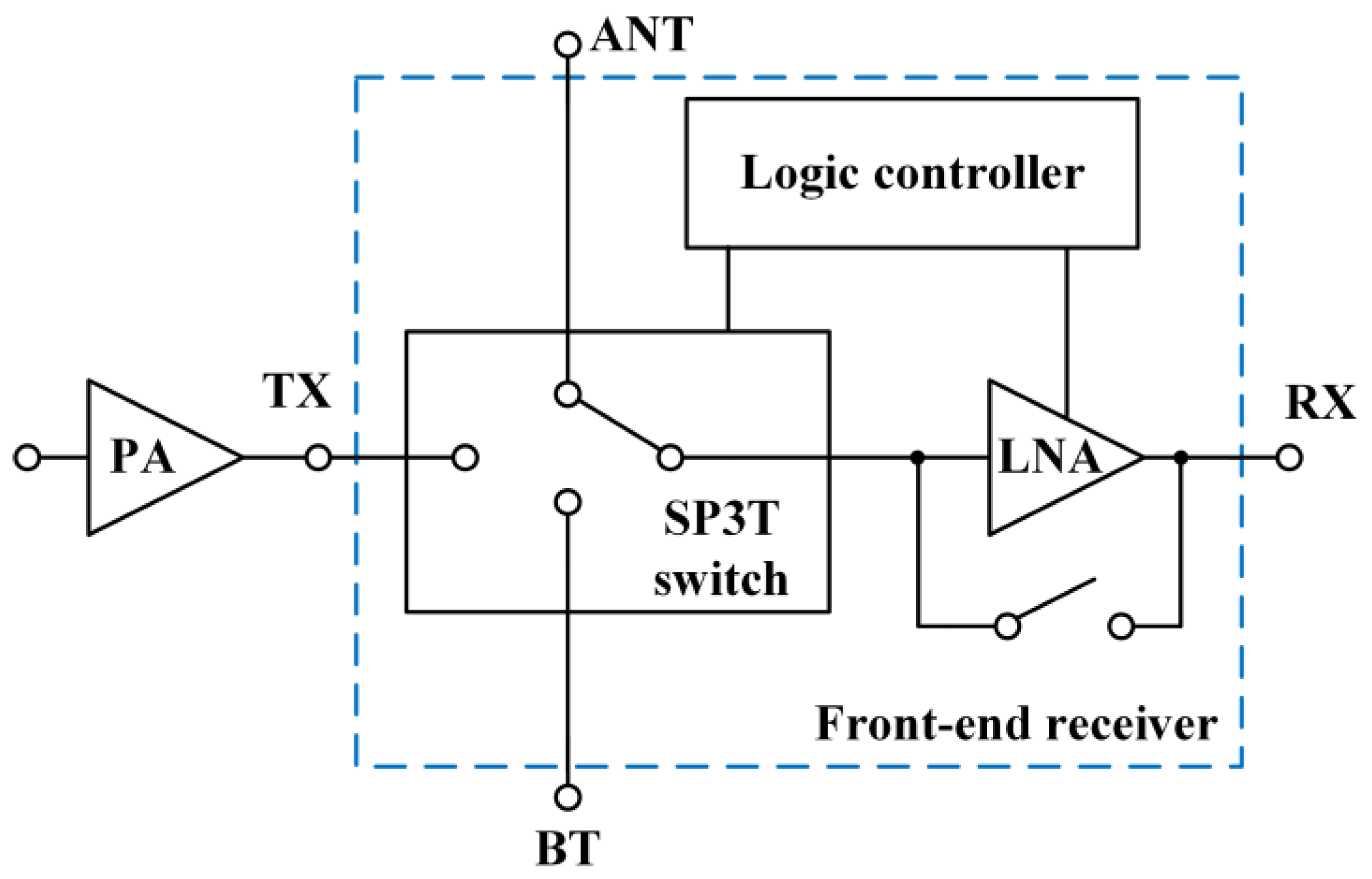
To obtain good RF performance and high integration, a fully integrated RF front-end receiver in WLAN system, including a LNA and a SP3T switch with logic controller incorporated for 2.4 GHz WLAN and Bluetooth applications, as shown in Figure 1, is proposed. The WLAN system has a transmitting path and a receiving path. A power amplifier (PA) is used in the transmitting path to amplify the signal from the inside system and send it via the antenna, while the LNA is used to receive a signal from the air space through antenna to inside the WLAN system. The SP3T switch is used to connect the antenna to the WLAN transmit-and-receive functions as well as Bluetooth functions in TDD frond-end transceivers.
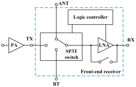
Figure 1.
Block diagram of proposed front-end receiver for wireless local area network (WLAN) and Bluetooth applications.
As explained above, TX is the output port of the PA and one of the input ports of the SP3T switch. BT is the interface that is used to connect the antenna to the Bluetooth transmit-and receive-functions. ANT is a common port that is used to transmit and receive signals for both WLAN and Bluetooth systems.
The proposed receiver is capable of switching into four operating modes, including receive high gain, bypass, transmit switch and Bluetooth switch modes. The logic controller is used to convert the logic control signals and provide enable signals to the receiver for different operation modes. The truth table and interfaces for different operation are shown in Table 1, where “1” equals to 3.3 to 5.0 V and “0” equals to 0 to 0.2 V. In both high gain and bypass modes, the system is in the WLAN receiving state, then the signal comes from ANT to RX. In transmit switch mode, the system is in the WLAN transmitting state, then the signal comes from TX to ANT. In Bluetooth switch mode, the system is in the Bluetooth transmitting and receiving state, then the signal can be from BT to ANT and ANT to BT. It is worth noting that the Bluetooth mode certainly needs gain as the WLAN mode does, but the receiving gain, NF and linearity performance for WLAN system are much higher than in the Bluetooth mode, so an extra WLAN front-end module consisting of a transmitting PA and a receiving bypass LNA with switch is required. The PA and LNA functions for Bluetooth are all incorporated in the subsequent CMOS RF transceiver module. In this work, we focus on the frond-end receiver that integrating the LNA and SP3T switch. A trade-off between power handling and isolation is discussed in the asymmetrical SP3T switch architecture. Additionally, a cascode LNA topology is chosen due to its high output impedance and remarkable NF performance [11]. To optimize the gain and noise performance, the effect of impedance and voltage-gain behavior on the given LNA are explored.

Table 1.
Truth table and interfaces for different operation.
2. Circuit Design
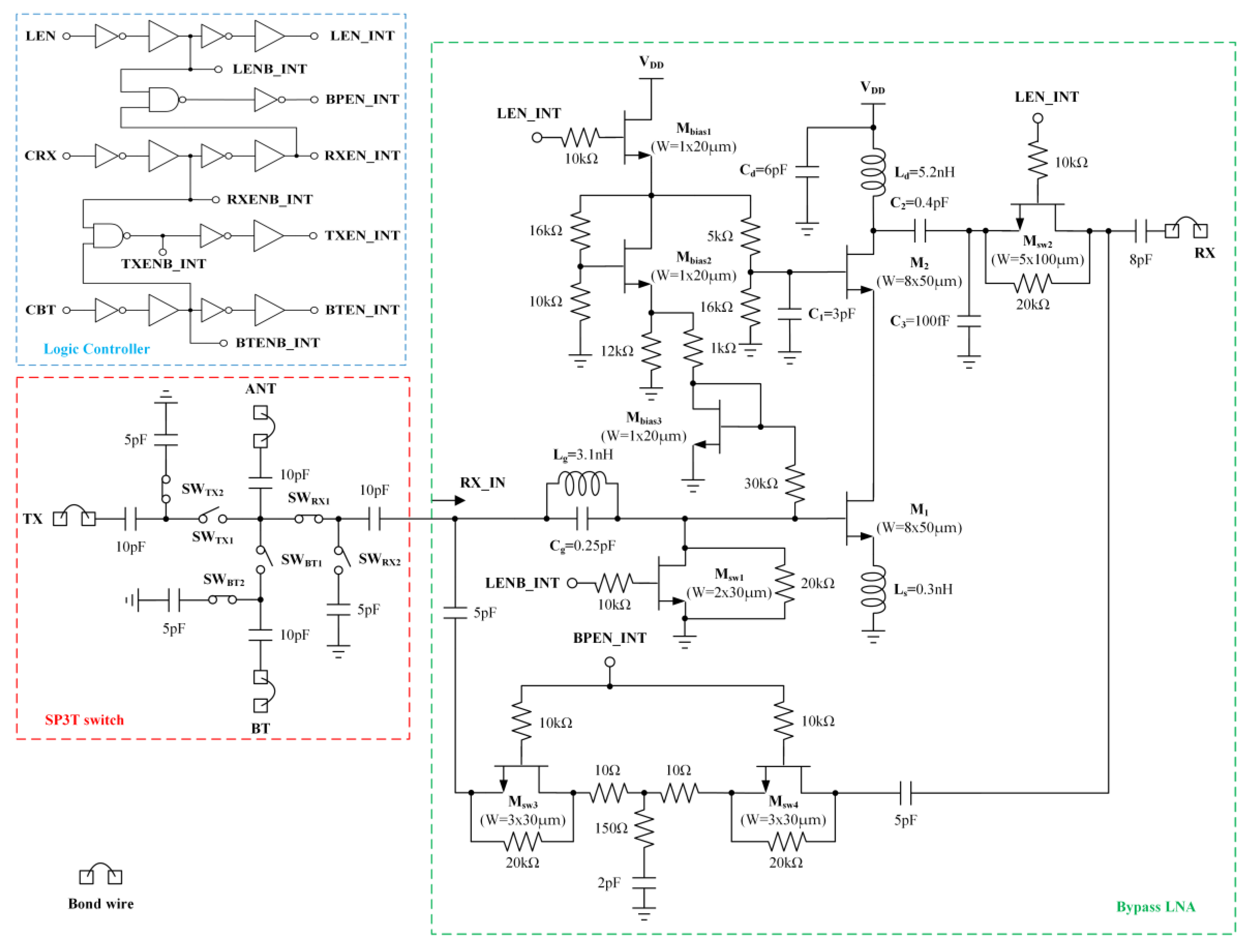
As shown as Figure 2, the proposed front-end receiver is divided into three main parts, a SP3T switch, a bypass LNA with bias circuitry and a logic controller. The SP3T switch is implemented to provide signal transmission channels for the bypass LNA, the PA and Bluetooth modules. The amplifier made in cascode structure selects and amplifies the 2.4-GHz signal which is driven by the bias circuitry consisting of a current mirror bias circuitry and a resistor divider. When a large power input signal is received, the LNA will switch to the bypass mode with 7–8 dB of loss to prevent damage of LNA itself and subsequent components such as the mixer. The logic controller converts three input logic control signals (CRX, LEN and CBT) into enable signals that allow the receiver to switch between four operating modes. The basic logic gates, including inverter, buffer and NAND gate of the logic controller are realized using both 0.25 μm E-mode and 0.5 μm D-mode pHEMTs.
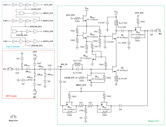
Figure 2.
Overall schematic of proposed front-end receiver.
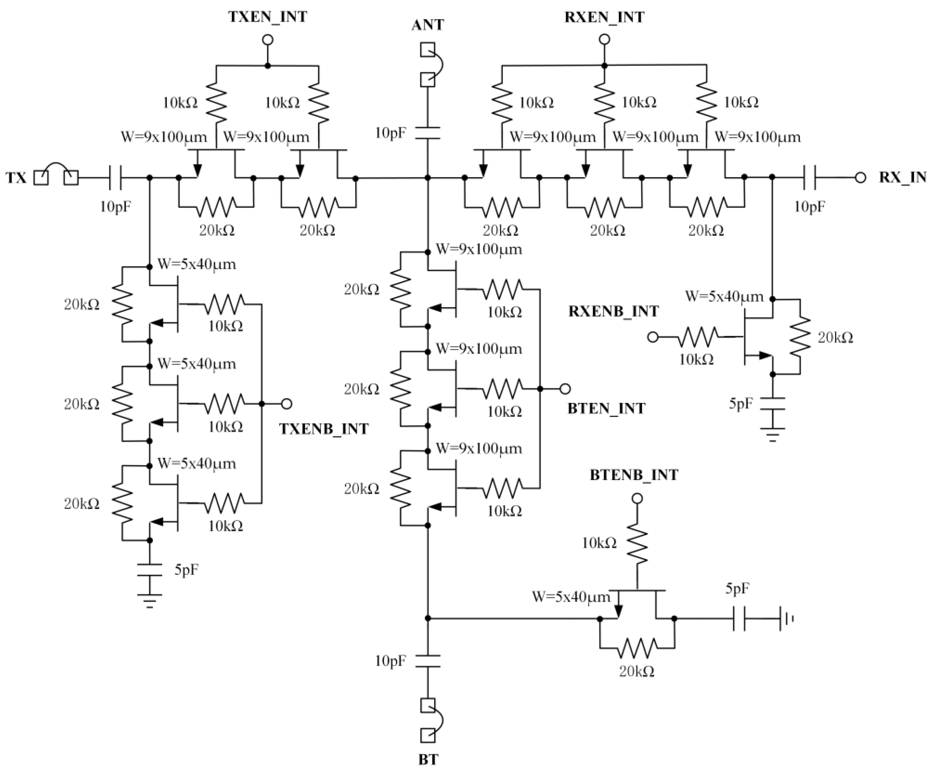
Figure 3 illustrates the detailed topology of the SP3T switch. In order to achieve low NF for the receiver LNA and high linearity for the transmit PA, as well as good isolation for the whole system, an asymmetrical series-shunt switch topology is adopted. In transmit switch mode, the switch needs to handle more than 30 dBm of input power as well as providing sufficient isolation between ANT and other ports during high-power signal transmission condition. Thus, three stacking transistors are employed for all the off arms to hold off the large power level when the transmit switch is on [12,13,14,15]. When the receive or Bluetooth switch is on, all off arms can utilize a smaller stack height since the power is much lower. Hence, only one device is employed for the receive and Bluetooth shunt arms, whereas two stacking transistors are used for the transmit series arm, taking into account the isolation between the transmit and receiving paths. Larger sizes of switch transistors can improve the insertion loss (IL) in on-state but would degenerate the required isolation in off-state. The width of series and shunt switch transistors with 0.5 μm D-mode pHEMTs are optimized as 900 μm and 200 μm, respectively. Additionally, a 20k Ω resistor is connected in parallel across the switch FET to share the large voltage swing when the switch transistors in off-state [12]. The operating states of all the series and shunt switch arms in four modes are shown in Table 2. All RF paths are DC blocked using series metal-insulator-metal (MIM) capacitors.
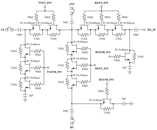
Figure 3.
Asymmetrical single-pole triple-throw (SP3T) switch topology.

Table 2.
SP3T switch operating state in four modes.
In receive high gain mode, the switch transistors Msw1, Msw3 and Msw4 are turned off while Msw2 is turned on, the signal from the ANT is fed into the receiving path, ensuring the signal to be amplified by the LNA to the output RX port. For high gain and good reverse isolation, an inductively source-degenerated cascode LNA structure is adopted to propose a solution to the dilemma of matching the input and noise impedance with the source of 50 Ω simultaneously [16,17]. The effect of the pHEMT M1 on the input impedance can be minimized by introducing an inductor (Lg) [18,19].
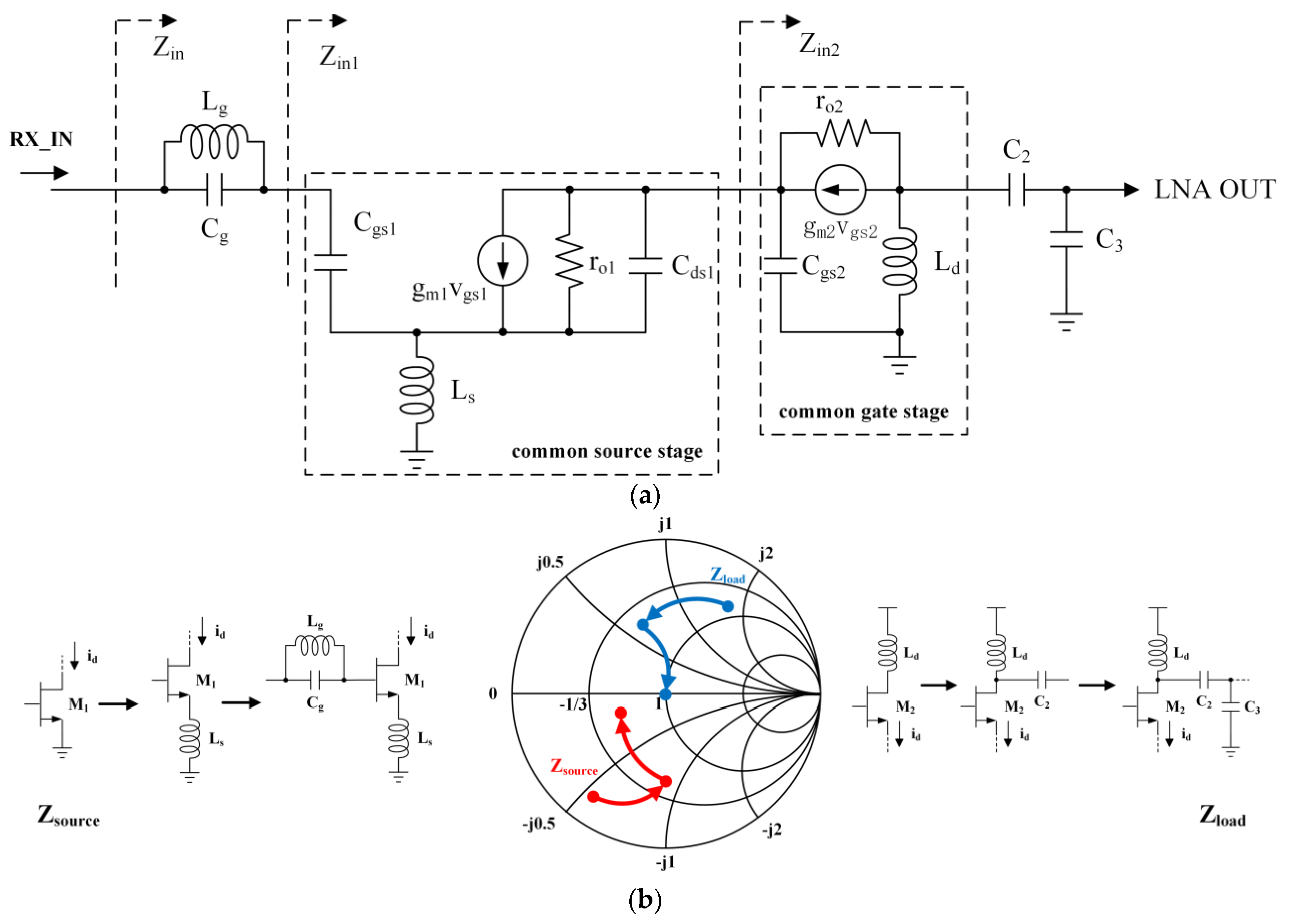
The configuration of matching networks and impedance traces of the proposed LNA are depicted in Figure 4. The input impedance of the entire cascode LNA including input and output matching networks, Zin, the input impedance of the common source (CS) amplifier, Zin1, and the input impedance of common gate (CG) amplifier, Zin2, can be written as:
where gm1 and gm2 are the transconductances, and ro1 and ro2 are the channel resistances of the CS and CG transistors, respectively. Cgs1 is the gate-to-source parasitic capacitance of the CS stage. It is easy to prove that the output impedance of the CS stage is given by
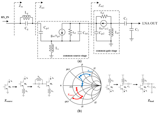
Figure 4.
(a) Small-signal equivalent circuit of proposed low-noise amplifier (LNA) circuit, (b) configuration of proposed impedance traces.
Thus, the voltage gain of the CS stage without input matching network can be derived as:
The voltage gain of the CG stage can be expressed as:
Based on Equations (1), (5) and (6), the input impedance can be matched to 50 Ω for maximum gain. However, apart from input impedance matching, modern LNA design also adopts noise cancellation to alleviate the trade-off between NF and S11 [20,21,22,23,24]. Based on the circuit connection shown in Figure 4, the noise contribution of the transistors including M1 and M2 are considered in the design [25,26]. The contribution of the CS stage to the output noise voltage is expressed as:
where k represents the Boltzmann’s constant, and T represents the absolute temperature.
The output noise voltage of CG stage can be expressed as:
Hence, the overall NF of the proposed LNA can be derived as:
Based on Equations (1) and (9), we optimize the input impedance and noise impedance to be close to the source impedance of 50 Ω by selecting a periphery of 8 × 50 μm with 0.25 μm E-mode pHEMT for the CS transistor. Here, Ls = 0.3 nH, Lg = 3.1 nH and Cg = 0.25 pF. It is notable that device cannot be sized too small due to the input P1dB constraint [3]. There is a trade-off between DC power consumption and power handling performance. For the given LNA, the input matching circuit dominates the NF performance, while the output matching has sight effect on the noise [27,28]. Therefore, the gain is mainly considered in the output matching. The load inductor Ld (5.2 nH), capacitance C2 (0.4 pF) and parasitic capacitance of M2 are resonated at operating frequency of 2.4 GHz.
Since the DC power is mainly sensitive to the bias of the CS stage, a current mirror bias circuitry is used for the CS transistor while a resistor divider is utilized for the bias of the CG stage.
Considering the receiver will obtain large signal when it closes to a signal source such as base station, a bypass function is incorporated into the LNA module which enables the LNA to switch into loss mode [29]. In bypass path, the switch Msw1, Msw3, Msw4 are in the on-states and Msw2 is in the off-state, a series of two transistors with sized 90 μm and T-type attenuation are employed to maintain the required loss of 7 dB while providing sufficient isolation between the input and output of the LNA. The operating state of four switches in receiving path has been extracted in Table 3.

Table 3.
Operating state of four switches in receiving path.
3. Measurement Results
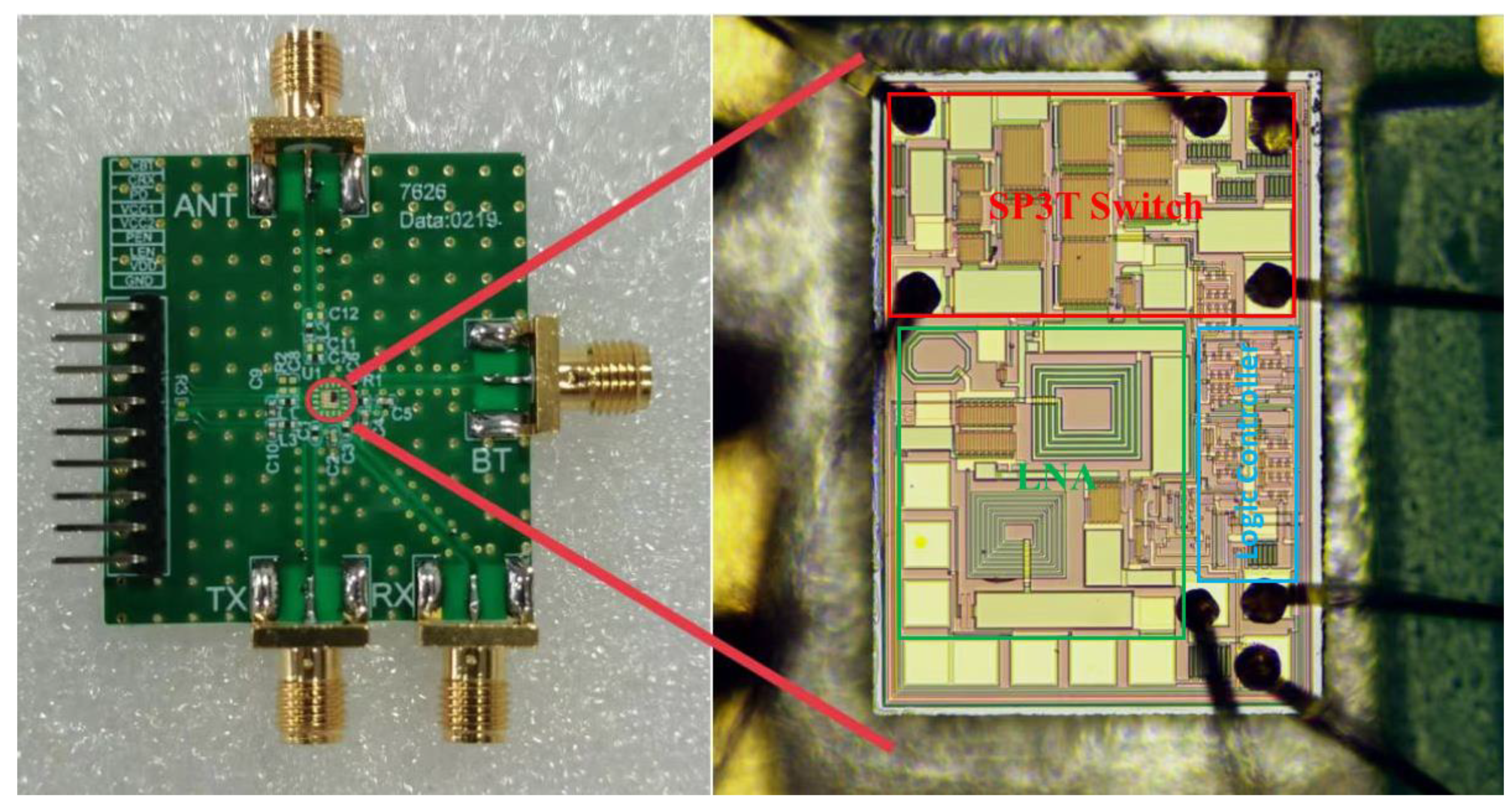
Figure 5 reveals a chip photograph of the proposed front-end receiver on a printed circuit board (PCB), which was provided by a foundry named Huanzhou Lion in mainland China with both 0.25 μm E-mode and 0.5 μm D-mode pHEMTs. All measured results are obtained taking into account the effect of the full evaluation board and the block diagrams of measurement setup are shown in Figure 6.
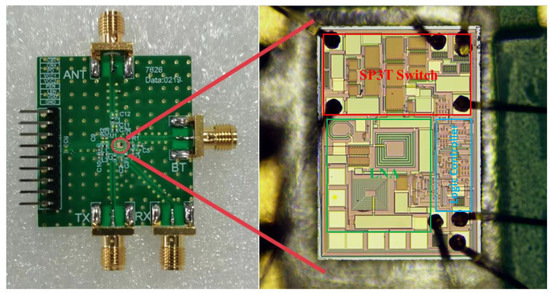
Figure 5.
Chip photograph of proposed front-end receiver on an evaluation board.

Figure 6.
Block diagrams of measurement setup of (a) S-parameters, (b) noise figure (NF) and (c) large signal performance.
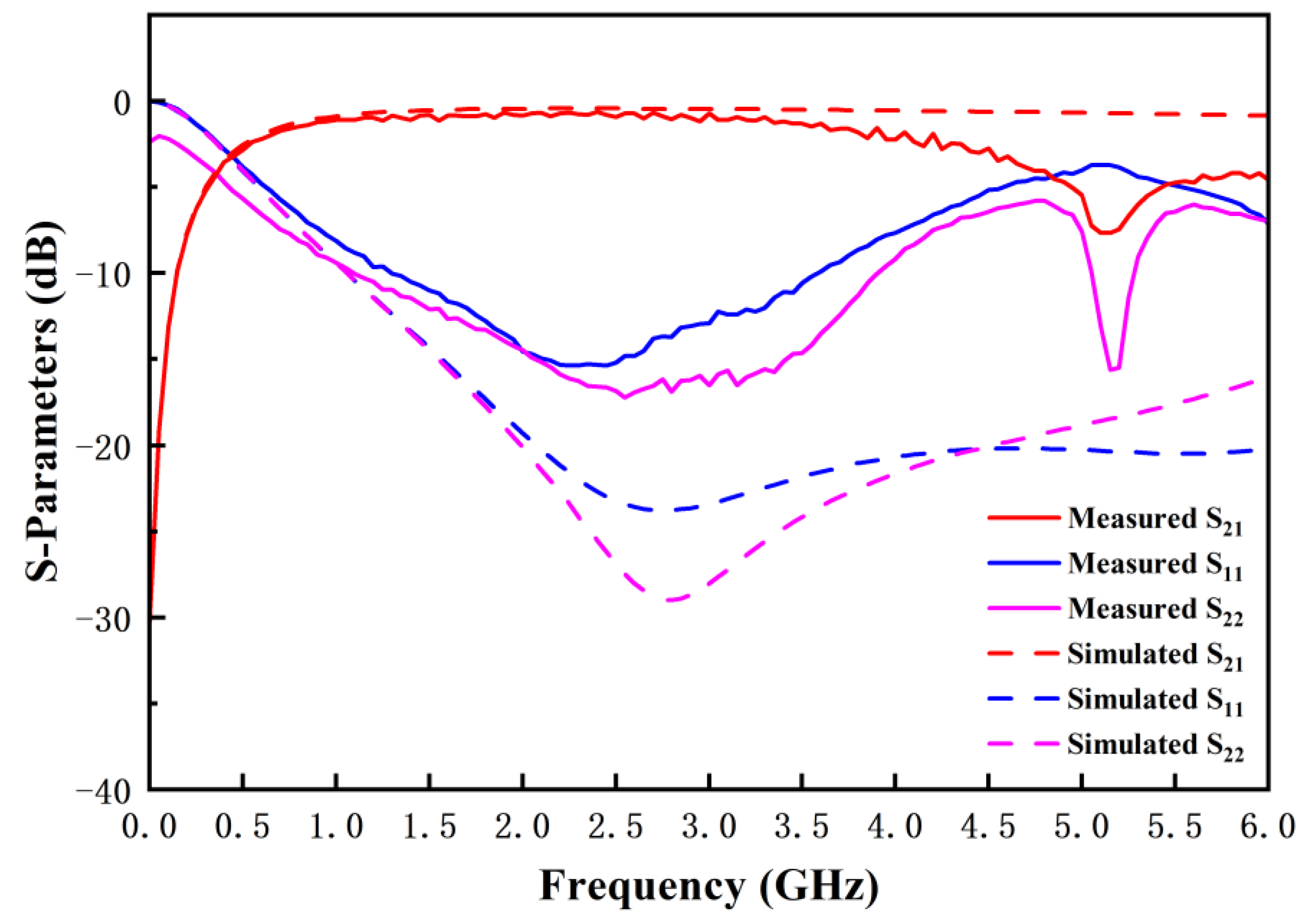
The S-parameters of the proposed receiver were measured using Keysight E5071C ENA vector network analyzer, as depicted in Figure 7, Figure 8, Figure 9 and Figure 10. In this study, the circuit simulations were performed using Keysight’s Advanced Design System software with a GaAs pHEMT design kit. The effect of the bond wire has been taken account in simulation. In high gain mode, the LNA achieves power gain of 20 dB at 2.4 GHz drawing 11 mA of current from 5 V power supply as shown in Figure 7. The lower and upper 3-dB bandwidth points are 2.2 and 3 GHz, respectively. In bypass mode, the LNA has an IL of 7.5 dB as shown in Figure 8. The measured IL is 0.6 dB at 2.4 GHz in transmit switch mode while 0.8 dB in Bluetooth switch mode as shown in Figure 9 and Figure 10, and the switches can handle more than 33 dBm of input power. It is obvious that all measured input and output return losses had exceeded 10 dB at 2.4 GHz with fully on-chip impedance matching networks.
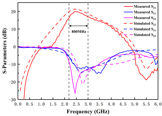
Figure 7.
Measured and simulated small-signal S-parameters of proposed front-end receiver in high gain mode.
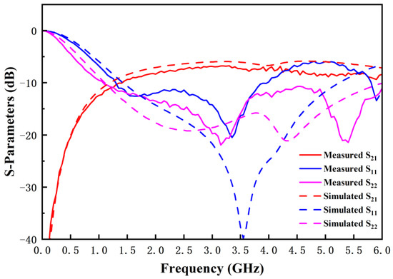
Figure 8.
Measured and simulated small-signal S-parameters of proposed front-end receiver in bypass mode.
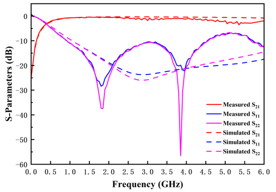
Figure 9.
Measured and simulated small-signal S-parameters of proposed front-end receiver in transmit switch mode.
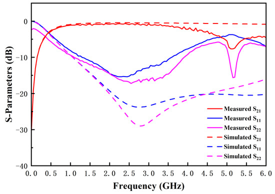
Figure 10.
Measured and simulated small-signal S-parameters of proposed front-end receiver in Bluetooth switch mode.
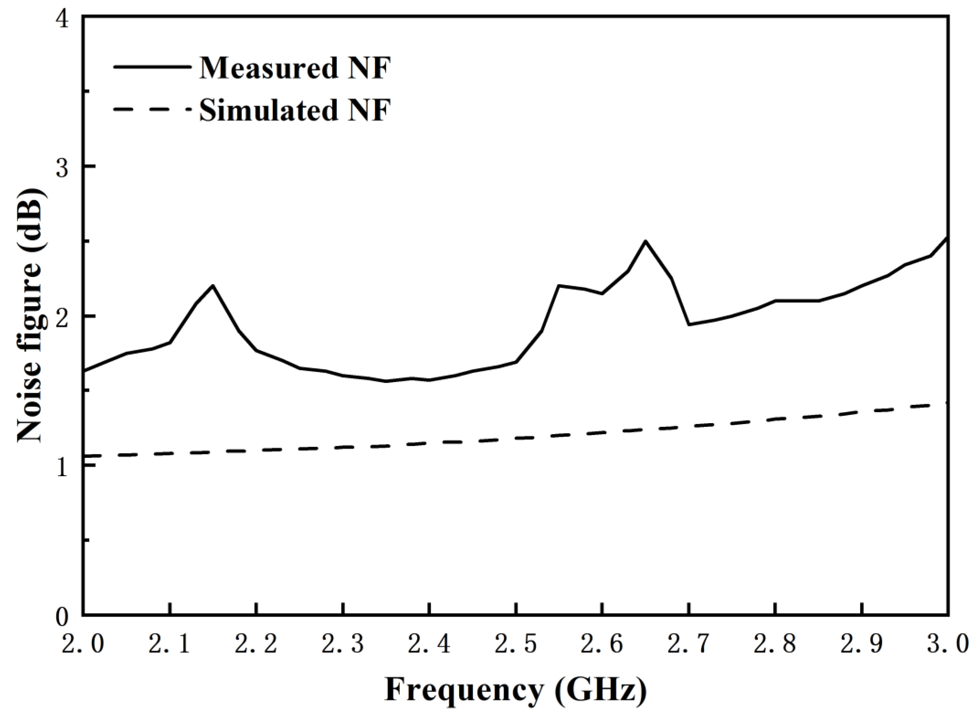
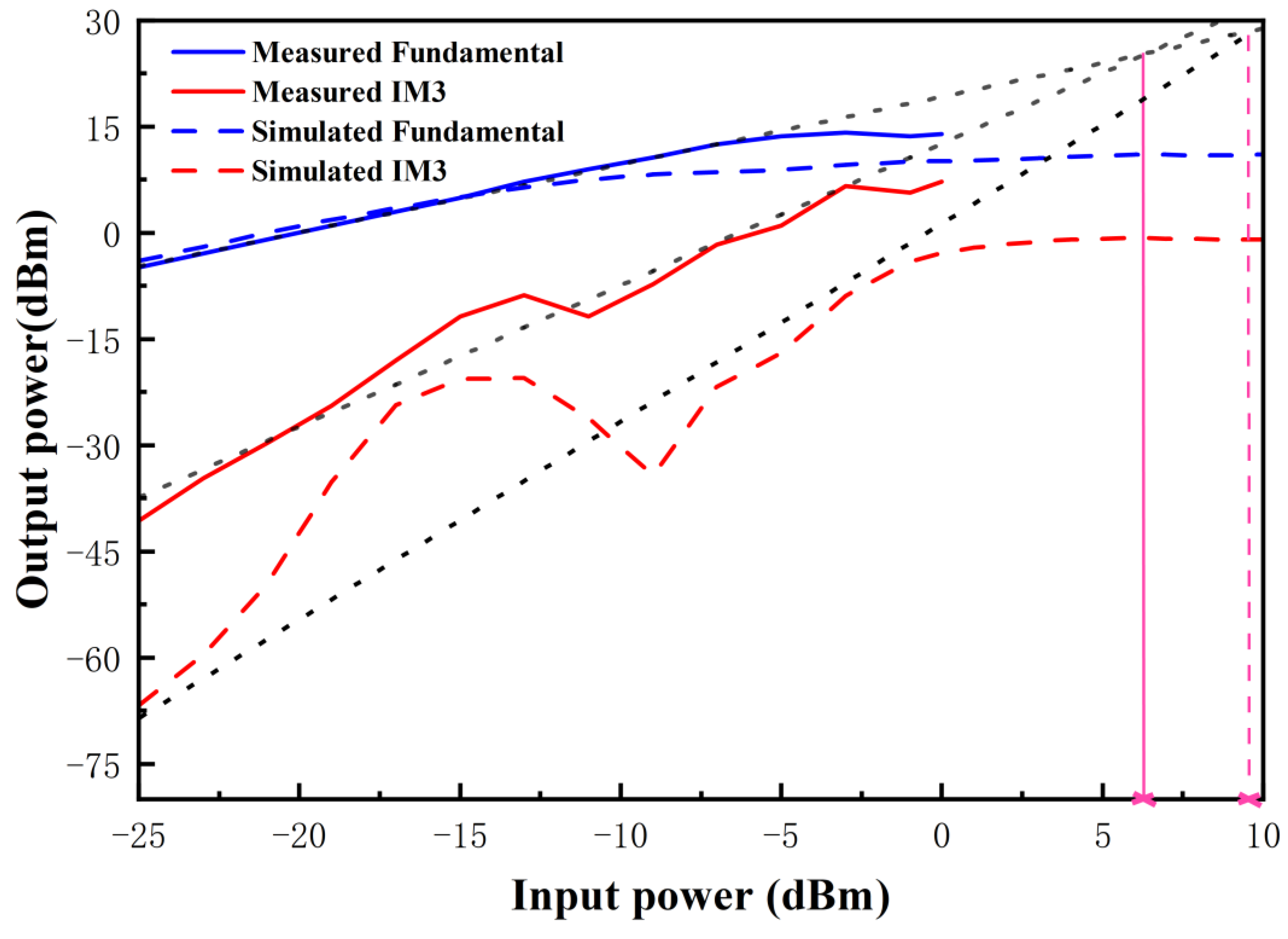
The NF and large signal parameters for linearity were measured using an Agilent N9030A PXA signal analyzer with Agilent 346B noise source and Agilent E4438C ESG vector signal generator. Figure 11 exhibits that the measured NF is below 1.7 dB in high gain mode for 2.4–2.5 GHz. Power handling capability of the LNA is critical for WLAN applications in order to avoid LNA compression and preserve the modulated signal received at the front-end. Figure 12 illustrates that the IIP3 of the LNA in high gain mode is 6dBm with the condition that the two-tone frequencies are 2.37 GHz and 2.43 GHz, respectively.
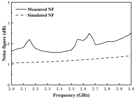
Figure 11.
Measured and simulated NF of proposed front-end receiver in high gain mode.
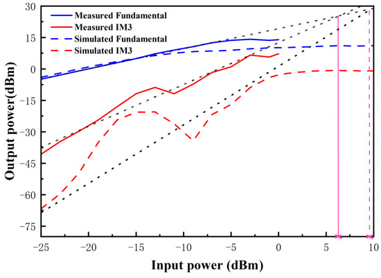
Figure 12.
Measured and simulated input third-order intercept point (IIP3) of proposed front-end receiver in high gain mode.
Table 4 compares the performance summary between the proposed RF front-end receiver and other state-of-the-art studies. The figure of merit (FOM) factor listed in the last row represents the comprehensive performance of the references. Here, the FOM is expressed as follows:
where G represents the voltage gain of the referred LNA in magnitude, and (NFmin-1) represents the excess noise factor in magnitude. Comparing the performance in terms of power gain, NF and cost, the measured power consumption of the proposed front-end receiver is slightly large due to the additional logic controller for mode switching. The proposed design presents excellent performance according to the calculation of FOM. With fully on-chip input and output matching networks, as well as bias and logical circuitry, this receiver can demand the wireless 802.11 b/g standards.

Table 4.
Comparison with previous studies.
4. Conclusions
In this paper, a fully-integrated GaAs pHEMT front-end receiver including a SP3T switch and a LNA with bypass function with four operating modes at 2.4 GHz, fabricated in a 0.25 μm pHEMT process for an IEEE 802.11 b/g standard is presented. An asymmetrical SP3T switch architecture is realized to provide signal transmission path for LNA, and extra PA and Bluetooth modules. A compromise between maximum gain and minimum noise is implemented based on inductively source-degenerated cascode topology. The LNA also incorporates a bypass module to handle high power signals. An NF of 1.7 dB, a power gain of 20 dB and IIP3 of 6 dBm drawing 11 mA of current from 5 V power supply at 2.4 GHz are realized in LNA high gain mode. In bypass mode, the LNA has an IL of 7.5 dB. The measured IL of transmit switch is 0.6 dB at 2.4 GHz while 0.8 dB of Bluetooth switch. With critical on-chip matching to the antenna, the proposed front-end receiver is suitable for WLAN and Bluetooth applications.
Author Contributions
Conceptualization, R.Y. and Z.Z.; methodology, R.Y. and Z.Z.; software, R.Y. and Z.Z.; validation, R.Y., Z.Z. and H.X.; formal analysis, R.Y. and Z.Z.; investigation, R.Y. and Z.Z.; resources, Z.Z. and G.Z.; data curation, R.Y. and Z.Z.; writing—original draft preparation, R.Y.; writing—review and editing, R.Y., Z.Z., H.X. and G.Z.; visualization, R.Y. and Z.Z.; supervision, Z.Z. and G.Z.; project administration, Z.Z. and G.Z.; funding acquisition, Z.Z. and G.Z. All authors have read and agreed to the published version of the manuscript.
Funding
This work was supported in part by the National Key R&D Program of China (Grant No. 2018YFB1802000), the National Natural Science Foundation of China (Grant No. 61974035), and the Guangdong Local Inno. Research Team of Pearl River Talent Program (Grant No. 2017BT01X168).
Institutional Review Board Statement
Not applicable.
Informed Consent Statement
Not applicable.
Data Availability Statement
The data may be obtained from the authors upon request.
Conflicts of Interest
The authors declare no conflict of interest.
References
- Yeh, Me.; Tsai, Zu.; Liu, Re.; Lin, K.-Y.; Chang, Y.-T.; Wang, H. Design and Analysis for a Miniature CMOS SPDT Switch Using Body-Floating Technique to Improve Power Performance. IEEE Trans. Microw. Theory Techn. 2006, 54, 31–39. [Google Scholar]
- Rao, C.V.N.; Ghodgaonkar, D.K.; Sharma, N. GaAs MMIC Low Noise Amplifier with Integrated High-Power Absorptive Receive Protection Switch. IEEE Microw. Wirel. Compon. Lett. 2018, 28, 1128–1130. [Google Scholar] [CrossRef]
- Madan, A.; McPartlin, M.J.; Zhou, Z.-F.; Huang, C.-W.P.; Masse, C.; Cressler, J.D. Fully Integrated Switch-LNA Front-End IC Design in CMOS: A Systematic Approach for WLAN. IEEE J. Solid-State Circuits 2011, 46, 2613–2622. [Google Scholar] [CrossRef]
- Pal, J.; Zhu, Y.; Lu, J.; Dao, D.; Khan, F. High Power and Reliable SPST/SP3T RF MEMS Switches for Wireless Applications. IEEE Electron Device Lett. 2016, 37, 1219–1222. [Google Scholar] [CrossRef]
- Joo, T.; Lee, D.-H.; Hong, S. A Fully Integrated RF CMOS Front-End IC for Connectivity Applications. IEEE Trans. Circuits Syst. II 2016, 63, 1024–1028. [Google Scholar] [CrossRef]
- Shi, J.; Yan, X.; Zhang, H.; Zhao, W.; Xia, X.; Lin, F. A 0.1–3.4 GHz LNA with Multiple Feedback and Current-Reuse Technique Based on 0.13-mm SOI CMOS. In Proceedings of the 2019 IEEE MTT-S International Wireless Symposium (IWS), Guangzhou, China, 19–22 May 2019; pp. 1–3. [Google Scholar]
- Kulatunga, T.; Belostotski, L.; Haslett, J.W. 400-to-800-MHz GaAs PHEMT-Based Wideband LNA for Radio-Astronomy Antenna-Array Feed. IEEE Microw. Wirel. Compon. Lett. 2018, 28, 909–911. [Google Scholar] [CrossRef]
- Fang, C.; Law, C.L.; Hwang, J. A 3.1–10.6 GHz Ultra-Wideband Low Noise Amplifier with 13-dB Gain, 3.4-dB Noise Figure, and Consumes Only 12.9 mW of DC Power. IEEE Microw. Wirel. Compon. Lett. 2007, 17, 295–297. [Google Scholar] [CrossRef]
- Ma, L.; Hale, C.; Baeten, R. A 1 mm2 Two Stage LNA and SP2T Switch RFIC FEM for WLAN 802.11a Applications. In Proceedings of the 2012 IEEE Radio and Wireless Symposium, Santa Clara, CA, USA, 15–18 January 2012; pp. 435–438. [Google Scholar]
- Wang, S. A GaAs MMIC LNA Design for Wideband Satellite Communication Receiver Application. In Proceedings of the 2014 IEEE International Conference on Communiction Problem-Solving, Beijing, China, 5–7 December 2014; pp. 631–633. [Google Scholar]
- Belostotski, L.; Haslett, J.W. Sub-0.2 dB Noise Figure Wideband Room-Temperature CMOS LNA With Non-50Ω Signal-Source Impedance. IEEE J. Solid-State Circuits 2007, 42, 2492–2502. [Google Scholar] [CrossRef]
- Shifrin, M.B.; Katzin, P.J.; Ayasli, Y. Monolithic FET Structures for High-Power Control Component Applications. IEEE Trans. Microw. Theory Techn. 1989, 37, 2134–2141. [Google Scholar] [CrossRef]
- Nguyen, D.P.; Pham, A.-V.; Aryanfar, F. A K-Band High Power and High Isolation Stacked-FET Single Pole Double Throw MMIC Switch Using Resonating Capacitor. IEEE Microw. Wirel. Compon. Lett. 2016, 26, 696–698. [Google Scholar] [CrossRef]
- Ayasli, Y.; Mozzi, R.; Hanes, L.; Reynolds, L.D. An X-Band 10 W Monolithic Transmit-Receive GaAs FET Switch. In Proceedings of the Microwave and Millimeter-Wave Monolithic Circuits, Arlington, Virginia, 6–7 May 1982; Volume 82, pp. 42–46. [Google Scholar]
- Huang, F.-J.; O, K.K. Single-Pole Double-Throw CMOS Switches for 900-MHz and 2.4-GHz Applications on p/sup-/Silicon Substrates. IEEE J. Solid-State Circuits 2004, 39, 35–41. [Google Scholar] [CrossRef]
- Lee, T.H. The Design of CMOS Radio-Frequency Integrated Circuits, 2nd ed.; Cambridge University Press: Cambridge, UK, 2003. [Google Scholar]
- Boglione, L.; Pollard, R.D.; Postoyalko, V. Optimum Noise-Source Reflection-Coefficient Design with Feedback Amplifiers. IEEE Trans. Microw. Theory Tech. 1997, 45, 402–407. [Google Scholar] [CrossRef]
- Aravinth Kumar, A.R.; Dutta, A.; Singh, S.G. A 1.5–7.5 GHz Low Power Low Noise Amplifier (LNA) Design Using Subthreshold Technique for Wireless Sensor Network (WSN) Application. In Proceedings of the 2012 IEEE International Symposium on Circuits and Systems, Seoul, Republic of Korea, 20–23 May 2012; pp. 1943–1946. [Google Scholar]
- Nguyen, T.-K.; Oh, N.-J.; Choi, H.-C.; Ihm, K.-J.; Lee, S.-G. CMOS Low Noise Amplifier Design Optimization Technique. In Proceedings of the 2004 47th Midwest Symposium on Circuits and Systems, Hiroshima, Japan, 25–28 July 2004; MWSCAS’04. Volume 1, p. I-185. [Google Scholar]
- Liao, C.-F.; Liu, S.-I. A Broadband Noise-Canceling CMOS LNA for 3.1–10.6-GHz UWB Receivers. IEEE J. Solid-State Circuits 2007, 42, 329–339. [Google Scholar] [CrossRef]
- Bruccoleri, F.; Klumperink, E.A.M.; Nauta, B. Wide-Band CMOS Low-Noise Amplifier Exploiting Thermal Noise Canceling. IEEE J. Solid-State Circuits 2004, 39, 275–282. [Google Scholar] [CrossRef]
- Chen, K.-H.; Liu, S.-I. Inductorless Wideband CMOS Low-Noise Amplifiers Using Noise-Canceling Technique. IEEE Trans. Circuits Syst. I Regul. Pap. 2012, 59, 305–314. [Google Scholar] [CrossRef]
- Lee, H.; Chung, T.; Seo, H.; Choi, I.; Kim, B. A Wideband Differential Low-Noise-Amplifier with IM3 Harmonics and Noise Canceling. IEEE Microw. Wirel. Compon. Lett. 2015, 25, 46–48. [Google Scholar] [CrossRef]
- Kim, J.; Hoyos, S.; Silva-Martinez, J. Wideband Common-Gate CMOS LNA Employing Dual Negative Feedback with Simultaneous Noise, Gain, and Bandwidth Optimization. IEEE Trans. Microw. Theory Tech. 2010, 58, 2340–2351. [Google Scholar] [CrossRef]
- Andreani, P.; Sjoland, H. Noise Optimization of an Inductively Degenerated CMOS Low Noise Amplifier. IEEE Trans. Circuits Syst. II: Analog. Digit. Signal Process. 2001, 48, 835–841. [Google Scholar] [CrossRef]
- Yeom, K.-W. Microwave Circuit Design: A Practical Approach Using ADS, 1st ed.; Pearson: New York, NY, USA, 2015. [Google Scholar]
- Razavi, B. RF Microelectronics (2nd Edition) (Prentice Hall Communications Engineering and Emerging Technologies Series), 2nd ed.; Prentice Hall Press: Toronto, ON, USA, 2011. [Google Scholar]
- Kwon, K.; Kim, S.; Son, K.Y. A Hybrid Transformer-Based CMOS Duplexer with a Single-Ended Notch-Filtered LNA for Highly Integrated Tunable RF Front-Ends. IEEE Microw. Wirel. Compon. Lett. 2018, 28, 1032–1034. [Google Scholar] [CrossRef]
- El-Gabaly, A.M.; Saavedra, C.E. Broadband Low-Noise Amplifier with Fast Power Switching for 3.1–10.6-GHz Ultra-Wideband Applications. IEEE Trans. Microw. Theory Techn. 2011, 59, 3146–3153. [Google Scholar] [CrossRef]
- Hale, C.; Baeten, R. A 1mm2 Flip-Chip SP3T Switch and Low Noise Amplifier RFIC FEM for 802.11b/g Applications. In Proceedings of the 2010 IEEE Radio and Wireless Symposium (RWS), New Orleans, LA, USA, 10–14 January 2010; pp. 208–211. [Google Scholar]
- Fox, T.; Giacchino, R. A Flip-Chip Single-Pole Three-Throw Switch with Integrated Bypass LNA for WLAN Applications. In Proceedings of the 2009 European Wireless Technology Conference, Rome, Italy, 28–29 September 2009; pp. 250–253. [Google Scholar]
Disclaimer/Publisher’s Note: The statements, opinions and data contained in all publications are solely those of the individual author(s) and contributor(s) and not of MDPI and/or the editor(s). MDPI and/or the editor(s) disclaim responsibility for any injury to people or property resulting from any ideas, methods, instructions or products referred to in the content. |
© 2022 by the authors. Licensee MDPI, Basel, Switzerland. This article is an open access article distributed under the terms and conditions of the Creative Commons Attribution (CC BY) license (https://creativecommons.org/licenses/by/4.0/).

