Featured Application
Two-dimensional materials-based devices and sensors.
Abstract
Molybdenum disulfide (MoS2) has been actively explored as a direct bandgap semiconductor in the monolayer (ML) limit for various applications due to its prominent physical properties and stability. In order to broaden its application range further, diverse treatments have been developed to modulate the properties of ML-MoS2. The native point defects, such as S vacancies, are known to activate surface charge transfer doping in ML-MoS2. Unlike conventional semiconductors, ML-MoS2 shows distinct excitonic transitions that can be exploited for controlling its optical, optoelectronic, and electric characteristics via coupling with defect-driven doping. Here, the ambient photoluminescence (PL) of ML-MoS2 could be increased by ~1500% at the center of focused-laser irradiation (FLI). Expectedly, the PL intensity varied spatially along with exciton–trion transitions across the irradiation spot due to the Gaussian profile of laser intensity. Then, nano-Auger electron spectroscopy (n-AES) revealed that the spectral fraction of exciton PL increased by ~69.2% while that of trion PL decreased by ~49.9% with increasing S deficiency up to ~13.4 ± 3.5%. Cryogenic PL and field-effect transistor experiments were also performed to understand the defect-related phenomena comprehensively. This novel experimental combination of FLI with an n-AES probe provides a facile, effective, and cost-efficient approach for exploring defect effects in two-dimensional structures.
1. Introduction
Two-dimensional (2D) molybdenum disulfide (MoS2), one of the semiconductor members of the 2D layered transition-metal dichalcogenide (TMDC) group, has been paid attention for fundamentally interesting phenomena such as indirect-to-direct crossover of the band structure in the monolayer (ML) limit, deep excitonic energy levels, strongly coupled valley, spin degree of freedoms, etc. [1,2,3]. Besides the basic scientific interests, as a promising alternative to conventional semiconductors in contemporary electronics for overcoming the fundamental limit of down-scaling, diverse electronic device applications have been developed actively from elementary device elements to complex digital circuits [4,5]. Moreover, the direct bandgap of ML-MoS2 enables miniaturizing photonic and optoelectronic integrated circuits [6]. In addition, 2D MoS2 structures are expected to be suitable for sensor applications since they show, as surface states themselves, extremely high surface area-to-volume ratio, outstanding sensitivity to the environment, and excellent chemical and mechanical stability [7,8,9,10]. Moreover, integrating the interactive 2D MoS2 layer into hetero-structures composed of other 2D layers or functional materials of other dimensions realizes novel synergetic applications such as flexible electronics and sensors, memory devices, and energy conversion systems [11,12,13,14,15]. However, it is still challenging to replace conventional materials whose synthesis, doping, and device fabrication processes are well-established in the modern industry. Therefore, for feasible applications, it would be required to enhance the functional capability of 2D MoS2 by tuning its properties controllably. For these purposes, various approaches have been developed: substitutional doping, nanostructure decoration, mechanical strain application, chemical surface functionalization, organic material coating, plasma and laser thinning, etc. [10,16,17,18,19,20,21,22].
One of the traits that make several TMDC MLs, including MoS2, WS2, MoSe2, and WSe2, distinguishable from conventional semiconductor materials such as Si is that excitonic transitions are active even at room temperature (RT) in ambient conditions due to extraordinarily huge binding energy and long lifetime of excitons [2,7,23]. In the case of ML-MoS2, its optical and optoelectronic properties can be governed by the transition between neutral excitation (A) and negatively charged exciton (A−), also referred to as trion [2,7,23]. The effects of the A–A− transition are controllable by charging/discharging ML-MoS2 via various methods such as electrostatic gating, interplay with phase change materials, gas molecule physisorption, metal nanoparticle coating, etc. [2,7,20,24]. Further, the charge transfer between ML-MoS2 and physisorbed gas molecules could occur more actively with defects [7,25,26]. The sulfur (S) vacancies are known to exist in ML-MoS2 as one of the primary native point defects based on the direct observation of transmission electron microscopy (TEM) as well as theoretical calculations [27,28,29]. These point defects tend to transfer electrons to physisorbed reactive molecules such as O2 and H2O and specific organic molecules, including single-layer titanyl phthalocyanine, leading to p-type doping as well as the transition from A− to A in ML-MoS2 [7,25,26,29,30,31].
Therefore, defect engineering, specifically controlling the amount of S vacancies, could be an efficient method to alter the optical, optoelectronic, and electrical properties of ML-MoS2 and also sensitivity to environmental conditions [25,27,28,32,33,34,35,36,37,38,39]. The defects, including S vacancies, have been shown to be created in diverse ways: thermal annealing, plasma treatment, irradiation with electrons, ions, and laser, etc. [25,32,33,35,36,37,38]. Above all, laser heating has been broadly employed for materials processing including deposition, selective melting, microstructural modification, fusion, etc. [40,41,42]. Specifically for 2D layered structures, laser irradiation would be a facile and versatile tool that can activate surface reactions such as atomic dissociation and substitutional doping as well as achieve structural modification from gentle thinning to sharp patterning [18,20,22,32,36,37,38,43,44]. Further, by employing a focused-laser beam, defects can be created locally, probably relevant to miniaturized devices or sensor applications [32,36,37,38]. Moreover, the detailed adjustment of laser processing parameters enables the subtle control of defect concentration minimizing the radiation and heat-induced damage [32,36].
However, to understand the defect-related effects fully, it would be necessary to perform a chemical analysis. Since 2D structures are surface themselves, the surface chemical analysis should be employed to probe their chemical state precisely. There are many options for surface chemical analysis on 2D materials: Auger electron spectroscopy (AES), x-ray photoemission spectroscopy (XPS), secondary ion mass spectroscopy (SIMS), etc. [17,43,45,46,47]. On a TEM, the crystal structure of 2D materials can be observed directly in atomic resolution, and elementary chemical analysis can also be carried out by energy-dispersive X-ray spectroscopy (EDS) using the electron beam as a radiation source [17,21,48].
In this work, nano-AES (n-AES), the high-resolution version of AES, was employed for the chemical analysis of ML-MoS2 for several advantages. As described in Figure 1a, the n-AES is equipped with a field emission gun (FEG) scanning electron microscope (SEM) as an electron beam source, which enables sub-micron lateral resolution of ~10 nm, much higher than those of XPS and SIMS. Moreover, a sample can be measured as it is on the n-ASE system without any additional laborious and costly sample preparation process that may result in damage and contamination. In addition, since the n-AES system is equipped with the SEM imaging capability, micro-size mechanically exfoliated ML-MoS2 flakes and even their internal structures can be accessed for spectra acquisition in the accuracy of sub-micron. The chemical properties of a variety of low-dimensional materials and nanostructures were probed by n-AES previously [25,32,49,50]. As displayed in Figure 1b, the Auger electrons are ejected by a two-step and three-electron process called the Auger effect. First, the core hole is created by the incidence beam of electrons (or photons for other cases). Then, an electron fills the core hole by the internal transition losing an amount of energy. If the transition energy is large enough to release another electron at the second outer shell, the electron can be ejected. The ejected electron, called the Auger electron, has the kinetic energy () as , where is the core hole energy level and and are the binding energies of the first and second outer shells, respectively [45].
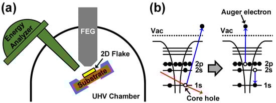
Figure 1.
(a) Illustrative diagram of the nano-Auger electron spectroscopy (n-AES) system equipped with a field emission gun (FEG), a hemisphere energy analyzer, an ultra-high vacuum (UHV) chamber, a sample stage, etc. (b) Schematic views of the two-step Auger electron emission process. Vac indicates the vacuum level.
While the focused-laser-assisted defect engineering and relevant phenomena were studied previously by several research, the combinational approach of focused-laser irradiation (FLI) and nano-Auger probe has not been reported yet to my knowledge [32,37,38]. Here, the FLI was demonstrated for creating defects in ML-MoS2 locally and tuning ambient optical and electrical properties of ML-MoS2 via defect-assisted p-type doping. The Gaussian laser intensity profile could build up a temperature gradient around the irradiation spot, resulting in the spatially varying degree of S deficiency in ML-MoS2 in a few microns. As such, microscale gradations of optical and electrical properties could be realized as well. Then, the varying local S deficiency was probed across the irradiation center by performing the high-resolution n-AES successively. Therefore, the detailed relationship between the ambient micro-photoluminescence (micro-PL) characteristics and defect state could be acquired in the wide range of S deficiency from only one sample by a one-off FLI process. Therefore, this approach provides a facile, effective, and cost-efficient way to explore defect-related phenomena in 2D structures.
In addition, cryogenic micro-PL spectroscopy and field-effect transistor (FET) device studies have also been carried out to comprehensively understand and validate the effects of the FLI-driven defect engineering on the physical properties of ML-MoS2. The cryogenic micro-PL experiments confirmed that, as approaching the irradiation spot, the defects were formed more actively in terms of the defect-related PL peak intensity. It was also observed that as ML-MoS2 was irradiated harder, the sensitivity of ML-MoS2 with air gas was enhanced. In the use of FET devices based on ML-MoS2 channels, the electrical FET device characteristics were also shown to be controllable by the FLI process showing p-type doping behavior consistently with the micro-PL characterization results.
2. Materials and Methods
2.1. MoS2 Monolayer Preparation
MoS2 flakes were prepared on 300-nm-thick SiO2/Si substrates by mechanical exfoliation with MoS2 single crystals (SPI Supplies, West Chester, PA, USA). Contact-mode atomic force microscopy (AFM) (Veeco Multiprobe system, Plainview, NY, USA) was conducted on the exfoliated MoS2 flakes to measure the thickness precisely as well as to monitor the surface topographical change by the FLI process.
2.2. Optical Characterization of MoS2 Monolayers
Both micro-PL and Raman spectroscopy experiments were carried out on ML-MoS2 flakes using a 100× objective lens (HC PL APO, 1.4 NA, Leica Microsystems Ltd., Wetzlar, Germany) on a confocal micro-Raman/PL system (invia Raman microscope, Renishaw, Wotton-under-Edge, UK) equipped with a motorized x–y axis stage, and a continuous-wave Ar-ion laser of the ~488 nm wavelength at RT in the ambient conditions. On the same system, low-temperature micro-PL spectroscopy was also performed on a sample loaded in a cryostat (ST-500, Lake Shore Cryotronics, Inc., Westerville, OH, USA) whose chamber was kept at the temperature of 77 K using liquid nitrogen as the coolant. The laser could be focused on a spot of the sample for the spectra acquisition in the use of a 50× long working distance objective lens (SLMPlan, 0.45 NA, Olympus Corp., Tokyo, Japan). The position of the spot could be located precisely by moving the whole cryostat on a manual x–y axis stage. The cryostat was pumped to ~10−6 Torr by a turbo pump system at 77 K. For comparison, the PL spectra of ML-MoS2 flakes in the cryostat were also measured at RT both in vacuum (~10−5 Torr) and air. The laser power was set in the range of 0.1–1 μW properly depending on the laser scan time and the number of scans to avoid any local damage and overheating in the samples. The laser spot sizes were ~0.4 μm and ~1.3 μm for the ambient micro-PL and cryogenic micro-PL characterization, respectively.
2.3. Focused-Laser Irradiation Process
The FLI process was performed in the home-built system equipped with a multichannel gas panel, a vacuum chamber, a dry pump system, a microscope, and a high-precision XY stage. The vacuum chamber was pumped to ~10−4 Torr and then filled with Ar gas maintaining the chamber pressure at ~400 Torr during the FLI process. A highly stable continuous wave 532 nm laser (diode-pumped solid-state laser, Lighthouse Photonics, San Jose, CA, USA) was focused onto a sample at the laser power of 250 W for 1 min. The laser beam was delivered through a 10× objective lens (Plan Apo, Mitutoyo, 0.28 NA, Kanagawa, Japan) with a laser spot size of ~2.3 μm. The laser irradiation conditions set in this work are the optimal parameters for maximizing the PL modulation given in the previous study [32]. No irradiation effect was activated at the laser power below 200 W. While the ambient PL intensity of ML-MoS2 increased as the laser power increased in the range of 200–250 W, it decreased at the laser power above 250 W. Finally, significant decomposition was detected on ML-MoS2 irradiated at the laser power of 300 W by the contact-mode AFM [32]. Further, to understand the irradiation process on MoS2 and other 2D materials more deeply, the effects of laser process parameters on laser absorption should also be considered carefully [51].
2.4. Nano-Auger Electron Spectroscopy
The local chemical properties of irradiated ML-MoS2 flakes were investigated by performing n-AES using a nano-Auger system (Oxford, Abingdon, UK/Scienta Omicron, Uppsala, Sweden) equipped with a FEG, which enables a spatial resolution of ~10 nm, as depicted schematically in Figure 1a. An ML-MoS2 flake was observed first at the proper magnification by SEM (Figure S1). The position of a spot was determined based on the SEM images, and then the electron beam was focused on the spot to acquire a spectrum. The spectra of ML-MoS2 were obtained in the constant retard ratio (CRR) mode with the retard ratio of 5. The nano-Auger system was operated at the accelerating voltage of 3 kV and under the ultrahigh vacuum (UHV) of <10−10 Torr. To avoid any damage or overheating by the electron beam, each spectrum was taken only for 7 secs.
2.5. Field-Effect Transistor Device Fabrication and Electrical Characterization
FET devices composed of ML-MoS2 channels and Ti/Au metal contacts (thickness: 10 nm/70 nm) were built up by a series of conventional fabrication processes of electron beam lithography (EBL), electron beam evaporation, lift-off process, etc. The ML-MoS2 channels underwent the FLI process prior to the fabrication process. Back-gated FET devices were characterized with the heavily doped p-type Si substrate as the bottom electrode on a probe station equipped with two programmable electrometers (617, Keithley, Cleveland, OH, USA) in the ambient conditions. By using the ST-500 cryostat, the back-gated FET measurements were also performed in the vacuum (~10−5 Torr) at RT. The FET devices were annealed gently at ~400 K for 4 h before the measurements in a vacuum to remove physisorbed molecules and contaminants on the ML-MoS2 surface or in the ML-MoS2/substrate interface.
3. Results and Discussion
3.1. Ambient Photoluminescence Characterization
As shown in the optical microscopy (OM) image of Figure 2a, several MoS2 flakes were prepared on a SiOx/Si substrate by the mechanical exfoliation method, and one of the MoS2 flakes was chosen for the FLI process. By comparing the contact mode, AFM images scanned from the region of the MoS2 flake, including the irradiation spot before and after the FLI process, as shown in Figure 2b,c, respectively, the surface of the MoS2 flake was found to be not damaged without any sign of significant decomposition of MoS2. Previously, J. Ru et al. demonstrated that the MoS2 films could be thinned by FLI [18]. In this work, by the gentle FLI process, only the contaminant residue along the edges of the flakes was observed to be removed, probably along with the creation of defects that is discussed later. In Figure 2d, the line profile across the MoS2/SiOx boundary extracted from the AFM image in Figure 2c shows that the MoS2 flake is ~0.6 nm thick and, therefore, ML-thick [2].
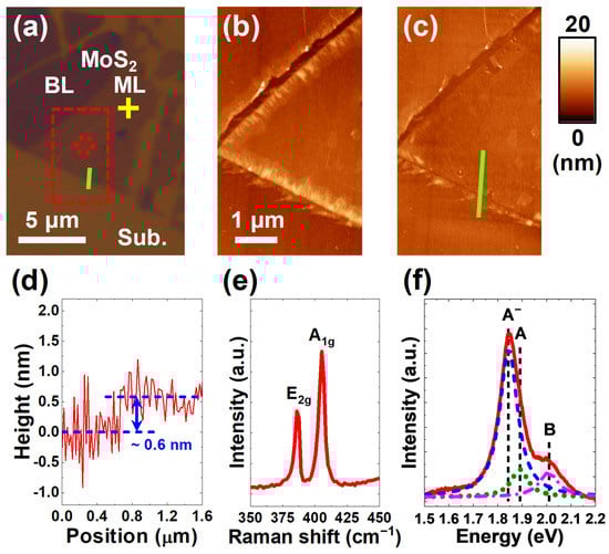
Figure 2.
Surface morphology and optical characteristics of MoS2 monolayer (ML) prepared by the mechanical exfoliation method: (a) An optical microscopy (OM) image to show the ML and bilayer (BL) regions of MoS2 flakes on 300-nm-thick SiO2/Si substrates Sub. The red dashed circle indicates the spot on the ML region treated by the focused-laser irradiation (FLI). The images of atomic force microscopy (AFM) were taken (b) before and (c) after the FLI process. The region of the red dashed rectangular (a) was scanned for the AFM images. (b,c) are presented in the same scales. (d) The AFM line profile was scanned along the green segment marked in (a,c) to confirm the irradiated MoS2 flake to be ML-thick (~0.6 nm). (e) Typical ambient Raman and (f) photoluminescence (PL) spectra measured from the pristine ML-MoS2 flake before the FLI process. The spot for spectrum acquisition is marked with the yellow cross in (a). In (f), based on the Lorentzian curve fitting, the PL spectrum can be de-convoluted to three subsidiary peaks (sub-peaks) contributed from the radiative recombination processes involved with neutral excitons (A), negatively charged excitons (also referred to as trions) (A−), and spin-orbit interactions (B), respectively.
In Figure 2e, the representative Raman spectrum measured from the pristine ML-MoS2 flake before the FLI process shows the typical Raman aspect of ML-MoS2, validating the crystal structure quality. Moreover, in Figure 2f, the PL spectra measured from the pristine ML-MoS2 flake in the ambient conditions showed a strong PL peak with a peak position of ~1.84 eV, representing the direct bandgap feature of the ML-MoS2 not shown from thicker MoS2 sheets. As described in Figure 2f, the Lorentzian curve fitting resolves the PL peak into three subsidiary peaks which originate with the radiative recombination processes of A (~1.89 eV), A− (~1.84 eV), and spin-orbit interactions (B) (~2.01 eV), respectively.
First, the area-selective modulation of ambient PL by the FLI process and relevant mechanisms is discussed. Figure 3b,c show the maps of the total integrated PL intensity, , acquired from the MoS2 flakes shown in Figure 3a before and after the FLI process in ambient conditions. The area-selective enhancement of ambient PL intensity is clearly observed around the laser-focused irradiation spot on the ML-MoS2 flake. The shape of the PL-enhanced area is shown to be irregular, probably because the laser-driven heat was not transferred uniformly in all directions from the irradiation spot due to structural imperfections, surface adsorbates, interfacial contaminants, etc. Moreover, the flake edges could be heated more intensively than the flake interior due to the difficulty in heat dissipation, as observed from the strong PL signal along the edge near the irradiation center in Figure 3c. The well-shaped PL-enhanced area was found in the other sample and will be discussed later. Figure 3d includes the Raman spectra measured before and after the FIR process at 6.0 μm near the irradiation center, where is defined as the distance from the origin 0 to a measured spot along the white dashed line in Figure 3c. In Figure 3d, as observed from the electron-irradiated free-standing ML-MoS2 by W. M. Parkin et al. and explained by their first-principles density function theory calculations, the red shift of the E2g peak by ~1.61 cm−1 indicates probably the partial absence of S including the formation of S vacancies, while the A1g peak does not show any obvious shift [33]. A. Bera et al. reported a similar red shift of the E2g peak of ML-MoS2 by FLI; however, they also observed that the A1g peak was blue-shifted clearly [36]. This discrepancy may be due to the fact that the peak shifts are also affected by other factors, including the change in the mechanical strain induced by substrates and the removal of surface and interface contaminants by FLI [10].
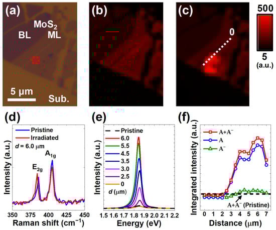
Figure 3.
Local modulation of ambient PL intensity of ML-MoS2 irradiated area selectively using the focused laser beam: (a) An OM image of the ML-MoS2 flake, including the red dashed circle, indicates the spot for the selective FLI process on the ML region. The maps of the total integrated PL intensity, , obtained from the ML-MoS2 (b) before and (c) after the FLI process. (a–c) are presented in the same scale, and (b,c) are drawn in the same color scale for the integrated PL intensity. (d) The Raman spectra were measured before and after the FIR process at 6.0 μm near the irradiation center. The parameter is the distance from the origin 0 to a measured spot along the white dashed line in (c). (e) A series of representative ambient PL spectra were measured by moving the focused-laser spot from the origin 0 to the spot of 7.0 μm across the irradiated region. (f) The variation in the integrated PL intensities of A and A− peaks, and , and their sum, , with . For a comparison, (e,f) include the data measured from the pristine ML-MoS2 before the FLI process.
A set of PL spectra were successively measured with the interval of 0.5 μm along the white dashed line in Figure 3c, moving the focused-laser spot from the origin 0 to the spot of 7.0 μm across the irradiated region. In Figure 3e, the representative PL spectra indicate that the ambient PL intensity was enhanced up to ~1500% in the vicinity of the irradiation center. The variation in the integrated PL intensities of A and A− peaks, and , and their sum, , are plotted with varying in Figure 3f. As expected, the substantial enhancement of the ambient PL intensity by the FLI process was likely to be caused by the defect-assisted evolution of A radiation represented by the sharp increase in near the irradiated spot, consistently with a similar laser process as well as other various defect creation methods, including global annealing, irradiation with alpha particles and electrons, etc. [7,25,26,32,33,36,37,38]. Further, in terms of the spectral fractions of A and A− peaks given in Figure 3f, the competitive contributions from and radiations to the ambient PL could be evaluated (Figure S2). In the un-irradiated region ( 2.5 μm) at some distance away from the irradiation spot, the A− radiation was dominant with the average spectral fraction of A− peak of ~71.5%, well consistently with that measured before the FLI process of ~74.9%. However, once the laser-treated region was reached with increasing , the spectral fraction of A peak increased abruptly, indicating the transition of A− to A. The average spectral fraction of A in the irradiated region ( 2.5 μm) was found to be ~87.6%, much larger than that of the pristine ML-MoS2 of ~18.4%. On the contrary, A− peak shows an average spectral fraction of only ~12.1% in the irradiated region, while ~62.0% in the pristine ML-MoS2. These results verify that the contribution of A recombination became overwhelming as the irradiation center was approached. The point defects, such as S vacancies, may interact with O2 and H2O molecules in the air resulting in the electron transfer from ML-MoS2 to the gas molecules [7,25,26,37]. Therefore, the increase in the amount of S vacancies by the FLI process leads to the augmentation of p-type doping effects accompanied by the active conversion from A− to A, consistently with previous defect engineering studies on ML-MoS2 [7,25,26,32,33,36,37,38]. The slight shift of the PL peaks to the lower energy is observed in the highly defective region of ML-MoS2, such as micro-cracks [26]. As shown in Figure 3e, the slight red-shift of the ambient PL peaks by ~0.04 eV was observed, indicating that the highly defective area was created area-selectively by the FLI process.
3.2. Chemical Analyses by Nano-Auger Electron Spectroscopy
Although the variation in optical properties of ML-MoS2 by the FLI process has been well-studied previously, often in terms of irradiation time, chemical analysis was usually missing or not in detail enough to correlate optical properties with defect states [32,36,37,38]. In this work, on the same locally irradiated ML-MoS2 sample, sub-nanoscale chemical analyses were conducted with the use of the n-AES technique. The n-AES spectra were measured successively by moving the focused electron beam along the white dashed line in Figure 3c from the origin 0 to the spot of ~6.41 μm with the interval of ~0.53 μm across the irradiated region (Figure S1). Figure 4a includes a set of representative n-AES spectra in the derivative form of vs. , where is the kinetic energy of detected Auger electrons, as designated previously, and is the number of detected Auger electrons dependent on , respectively. The strong peaks are related to the S LMM Auger transitions, while the two other peaks originated with the Mo MNN Auger transitions [45]. Since the peak-to-peak intensity, (i.e., the difference between the maximum point of the up peak and the minimum point of the down peak), is proportional to the number of elemental atoms related to the corresponding Auger transition [45]. Therefore, in this study, the of S LMM Auger transitions at 150.0 eV, , and that of Mo MNN Auger transitions at 186.5 eV, , were used for chemical analyses [45].
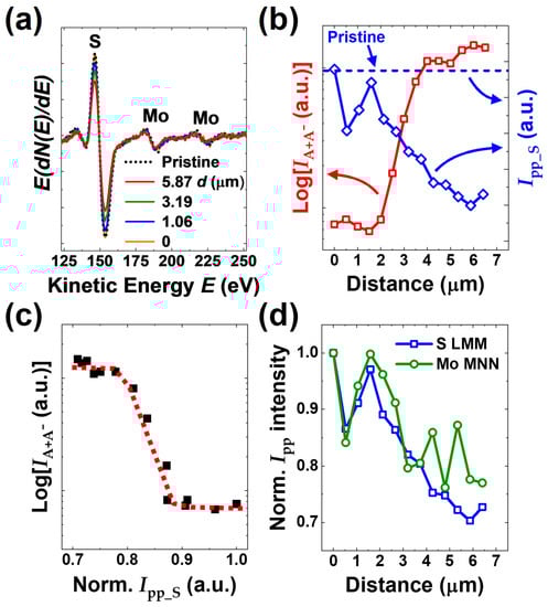
Figure 4.
N-AES analyses on the ML-MoS2 irradiated area selectively using a focused laser beam: (a) A set of representative n-AES spectra in the derivative form of vs. where and are the kinetic energy and the number of detected Auger electrons, respectively. These spectra were measured successively by moving the focused e-beam along the white dashed line in Figure 3c from the origin 0 to the spot of ~6.41 μm across the irradiated region. (b) The variations in and the peak-to-peak intensity of S LMM Auger signal, . (c) The data plot of vs. normalized to the value at . To match the two sets of data set for the same values, corresponding to the values for the data are given by linear interpolation. Note that the red-dashed curve is drawn only for guidance. (d) The changes in normalized peak-to-peak intensities, s, of S LMM (150.0 eV) and Mo MNN (186.5 eV) Auger signals with . For a comparison, (a,b) include the data measured from the un-irradiated region of pristine ML-MoS2.
In Figure 4b, the variations in two representative optical and chemical parameters, the of ambient PL and , respectively, with , are shown to be closely related to each other. As expected, when the decreased (i.e., the S deficiency increases), is enhanced, and vice versa. The plot of vs. normalized to the value at is also shown in Figure 4c. Since the two data sets were measured almost along the same white dashed line in Figure 3c but with different intervals, to match them with the same values, corresponding to the values for the data were determined approximately by linear interpolation. The ambient PL was observed to increase effectively when the normalized is lower than ~0.873, demonstrating that even the un-irradiated region of the ML-MoS2 flake not close to the irradiation spot has the fluctuation of the detected amount of S atoms as ~93.7 ± 6.0%, probably due to the existence of nanoscale defects such as nano-voids and nano-cracks, and local structural distortion by surface and interfacial contaminants [26]. Therefore, based on the plots of normalized s of S and Mo elements in Figure 4d, the actual S deficiency is determined to be ~13.4 ± 3.5% in the region around the irradiation center ( 3.5 μm), and similarly, the actual Mo deficiency is estimated to be ~6.4 ± 4.8%. By the FLI process, Mo defects seemed to be formed to some degree, although the Mo deficiency is not large like that of light S atoms. It is worth noting that the nanoscale fluctuation of the detected amount of atoms on ML-MoS2 revealed in this work should be considered carefully when 2D materials are analyzed by a chemical analysis tool of a relatively lower spatial resolution. Moreover, from Figure 4c, the PL intensity was found to be almost saturated below the normalized ~0.778.
3.3. Cryogenic Photoluminescence Characterization
In order to elucidate the defect-driven effects more clearly, a set of low-temperature micro-PL experiments were also carried out on another area-selectively irradiated ML-MoS2 flake displayed in the OM image of Figure 5a. As shown in Figure 5b, the map of of the ambient PL acquired on the ML-MoS2 flake after the FLI process shows the local enhancement of PL, similar to the previous results. The five positions a-e in Figure 5b were measured as the ML-MoS2 sample was loaded in the cryostat. In Figure 5c, the two pairs of PL spectra were measured in positions a (almost pristine region) and d (close to the irradiation spot) at RT in air and vacuum after gentle annealing at ~400 K, respectively. In a vacuum, both the two positions showed very low PL intensity with similar PL characteristics since the A radiation was suppressed in the absence of the interplay between S vacancies and O2 and H2O molecules in the air, as also observed in the previous studies [7,26,32,37]. However, once the ML-MoS2 was exposed to air, both two positions showed the augmentation of PL intensity but by different amplitudes. The variation in PL modulation in terms of was observed to be much large in position d than in position a by 2.5 times. The reason why the un-irradiated region also showed the modulation of PL as environment conditions would be the existence of thermodynamically native point defects such as S vacancies [7,25]. These results imply that the defect engineering by the FLI process may be available for enhancing the air gas sensing capability of ML-MoS2 as well as tuning its electronic state and optical properties.
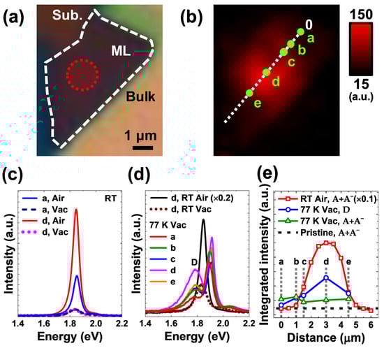
Figure 5.
Low-temperature micro-PL characterization of the area-selectively irradiated ML-MoS2: (a) An OM image of the ML-MoS2 flake, including the red dashed circle, which indicates the spot for the selective FLI process on the ML region. (b) The map of acquired after the FLI process. (c) Two pairs of PL spectra measured in the positions of a () and d ( μm) at room temperature (RT) in air and vacuum (Vac). (d) A series of PL spectra measured at 77 K in vacuum in the five different positions a–e along the white dashed line in (b) across the irradiated region. The positions b, c, and e are located at and μm, respectively. For comparison, the PL spectra measured in position d at RT in (c) are also drawn together. (e) The variations in at RT in air and at 77 K in vacuum and the integrated intensity of defect-activated peak (D), , with . For a comparison, (e) includes the ambient measured from the pristine ML-MoS2 before the FLI process at RT. Note that in (d), the peak height of the PL spectrum of the position d measured at RT in air is divided by 5, and in (e), at RT in air is divided by 10. Only the series of measurements at RT in air in (e) was carried out in the ambient, while all the other PL experiments were conducted on the sample in the cryostat.
As summarized in Figure 5d, a collection of PL spectra was measured at 77 K in a vacuum focusing the laser beam into the five different positions of the ML-MoS2 in the cryostat along the white dashed line in Figure 5b across the irradiated region. For comparison, the PL spectra measured in position d at RT in the air are also plotted together. At the low temperature, the defect-activated PL peak (D peak) was revealed clearly, and its PL intensity was observed to be stronger near the irradiation spot. Simultaneously, the main PL peaks were observed to be blue-shifted, possibly due to the temperature-dependent band structure of ML-MoS2 [25]. Moreover, its intensity became stronger in comparison to the PL at RT in a vacuum, probably due to the suppression of thermal effects such as phonon scatterings which hinder the radiation process [25]. In Figure 5e, the variations in at RT in air and at 77 K in a vacuum and the integrated intensity of D peak, , were plotted as a function of . Considering that both the defect-activated excitation in the low temperature and the defect-driven PL emission of A become more active with the higher concentration of defects, the strong correlation between and shown in Figure 5e are naturally accepted. These results also imply that the enhancement of air gas sensitivity is caused by the increase in S-deficiency via the FLI process. In addition, the profile of at RT in air in Figure 5e shows the well-defined peak shape. By the Gaussian fitting, the full width at half maximum (FWHM) of the fitted peak curve is determined to be ~2.4 μm, which is quite consistent with the laser spot size for the FLI process of ~2.3 μm. This agreement indicates that the distribution of defects related to the PL emission would follow the Gaussian profile of the laser beam intensity (Figure S3) [32].
3.4. Field-Effect Transistor Device Characterization
Lastly, the electrical characterization of FETs was also carried out in conjunction with the FLI experiments to demonstrate the area-selective modulation of electrical properties of ML-MoS2 channel-based FETs via laser-assisted defect engineering. As visualized in Figure 6a, the four FET devices (Dev1–4) were fabricated on a single partially irradiated ML-MoS2 with the same channel length () and width () as ~0.5 μm and ~3.5 μm, respectively. While the ML-MoS2 channel of Dev1 could be regarded to be almost pristine, that of Dev4 was irradiated intensively in the middle. Figure 6b shows a set of the drain current vs. gate voltage ( vs. ) plots measured from all devices in the range of from −100 V to 100 V at the drain-to-source voltage, , of 50 mV in ambient conditions. Following from the data, the devices behaved like the typical n-type channel FET with the large hysteresis, probably resulting from the surface adsorbates and interface contaminants [52]. The relatively low on–off ratio of ~103 of the Dev1 indicates that native point defects such as S vacancies may exist even in the un-irradiated channel leading to the p-type doping consistently with the PL results and could be improved if the physisorbed O2 and H2O molecules are removed by vacuum annealing [7,25]. The vacuum annealing effects on the FET devices based on the pristine and laser-irradiated channels can be found elsewhere (Figure S4 and Table S1). By the gentle vacuum annealing at 400 K, the hysteresis was observed to shrink significantly and then expand back slowly in the air. The on–off ratio was shown to be enhanced up to >104 (Figure S4). As shown in Figure 6c, the curves were also measured at 0 V for monitoring the variation in channel conduction by the FLI process as well as evaluating the performance of metal-ML-MoS2 contacts. It was clearly observed that the channel conduction decreased as the channels were irradiated more strongly, consistently with the trend of behaviors shown in Figure 6b. Further, the linearity of plots verify that the Ohmic contacts were formed across the metal-ML-MoS2 interfaces with negligible Schottky barrier during the FET device operation.
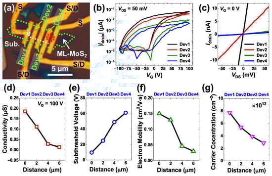
Figure 6.
Variations in field-effect transistor (FET) characteristics of ML-MoS2-based FET devices by the area-selective FLI process: (a) An OM plan-view image of the four FET devices (Dev1–4) based on a single ML-MoS2 flake. The red dashed circle indicates that the irradiation center was located inside the Dev4 channel. (b) The drain current vs. gate voltage ( vs. ) curves measured from the devices at the drain-to-source voltage () of 50 mV. (c) The set of vs. plots of the four devices at 0. From the vs. data in (b), the following important device parameters and electronic properties of the ML-MoS2 channels can be extracted: (d) channel conductivity () at 100 V, (e) subthreshold voltage (), (f) electron mobility (), and (g) electron carrier concentration (). The distance d in (d–g) indicates the locations of the Dev1–4 along the dashed line parallel to the channel length from the origin 0 in the center line of the Dev1 channel as described in (a). Note that in (g), the values should be multiplied by 1012.
The locations of the Dev1-4 are expressed by the d, which is defined as the distance from the origin 0 located in the center line of the Dev1 channel along the dashed line parallel to the channel length, as described in Figure 6a. Then, the irradiation effects on device parameters and properties of the ML-MoS2 channels are discussed based on the analyses of the data below. The on-state channel conductivity () for the 2D system is defined as where is the conductance at 100 V [53]. As the irradiation spot was approached from Dev1 to Dev4 (with increasing d), was observed to decrease monotonically by more than one order of magnitude from ~0.19 μS (Dev1) to ~0.014 S (Dev4), as shown in Figure 6d. In Figure 6e, the subthreshold voltage () was determined as the -axis intercept value of a linear fit to a curve in the linear regime [54]. The shift of to the direction of positive can be seen as the influence of irradiation becomes more significant with increasing d. These results can be interpreted as the p-type doping induced by the FLI process. The electron mobility () is given by the field-effect mobility, which is defined from the linear region of a curve with a slope of as where is the oxide capacitance per unit area [53]. Figure 6f shows that decreased from ~0.15 cm2/V∙s (Dev1) to ~0.03 cm2/V∙s (Dev4) as the irradiation effects were applied more significantly probably since the defect created by the FLI process may play a role as a scattering center or a carrier trap [55]. The relatively low RT is probably due to the interfacial charge traps between the MoS2 channel and substrate and is expected to increase with decreasing temperature by suppressing phonon scattering [53]. The could be enhanced by improving the metal/ML-MoS2 contacts, optimizing interface and surface states, and adopting the device design suitable for high-mobility devices [53,55,56,57]. Moreover, by gentle annealing, could be improved up to ~0.40–0.50 cm2/V∙s in the case of pristine channels (Figure S4).
More importantly, Figure 6g shows that the electron carrier concentration (n2D) for the 2D system calculated from decreased from 7.74 × 1012 cm−2 (Dev1) to 2.87 × 1012 cm−2 (Dev4) by ~62.9% with the irradiation intensity increases (with increasing ) [53]. The value in the pristine state (Dev1), quite consistent with the literature value of ~1013 cm−2, may justify these analyses based on the FET characterization [58]. Accordingly, it is verified that the p-type doping effects based on the interaction between point defects and gas molecules could be amplified by the FLI process [25,26,32]. Moreover, it should be noted that was degraded rapidly by the FLI process since both and decreased simultaneously. These results show that the FLI process enables tuning electrical device properties of ML-MoS2-channel-based FETs exploiting defect-assisted p-type doping effects, consistently with the results of ambient PL experiments. Via the advanced post-fabrication annealing process, it would be possible to improve the device performance of FLI-treated FET channels further in terms of hysteresis and .
4. Conclusions
In summary, the focused-laser-assisted defect engineering in ML-MoS2 was demonstrated, and its effects on the optical, chemical, and electrical properties of ML-MoS2 were investigated systematically. The gradations of ambient PL were created by the non-uniform distribution of irradiation intensity. The enhancement of ambient PL intensity along with the exciton–trion transitions was observed as the irradiation center was approached. These area-selective and controllable p-type doping effects are likely to be caused by the defect modification assisted by the focused laser beam. These defect-related doping phenomena were analyzed by probing the local elemental deficiency of ML-MoS2 flakes using the n-ASE technique, and their mechanisms were also corroborated by the cryogenic PL experiments and FET device characterization. Moreover, the augmentation of air gas sensibility was also achieved by activating the interactions between S vacancies and air molecules by this method.
In addition, large-area synthesis of various 2D materials has been researched actively [59]. In the case of the 2D TMDC group, including 2D MoS2, chemical vapor deposition (CVD) enables even wafer-scale epitaxial monolayer film growth [60]. The size and shape-related issues during focused-laser irradiation, such as overheating along flake edges and irregular heat transfer, are expected to be avoided on the continuous large-scale TMDC monolayer films. Therefore, applying this approach to CVD-grown 2D films would lead to performing more accurate and systematic defect studies as well as developing more practical device and sensor applications [59,60,61]. Further, beyond 2D materials, this approach based on the unique combination of experimental characterization techniques would be of high usefulness for exploring fundamental defect-related phenomena in reduced-dimension material structures as well as optimizing defect chemistry for the relevant applications.
Supplementary Materials
The following supporting information can be downloaded at https://www.mdpi.com/article/10.3390/app13010304/s1: Figure S1: Scanning electron microscopy (SEM) imaging for nano-Auger electron spectroscopy (n-AES); Figure S2: The spectral fractions of the ambient photoluminescence (PL) peaks contributed from the radiations of exciton (A) and negatively charged exciton (A−), also referred to as trion; Figure S3: The Gaussian profile of the ambient PL emission profile; Figure S4. Vacuum annealing effects on the field-effect transistor (FET) devices based on the pristine and FLI-treated ML-MoS2 channels; Table S1. Electronic characteristics of the pristine and irradiated ML-MoS2–based FET channels in vacuum and in air.
Funding
This research was supported by the Basic Science Research Program through the National Research Foundation of Korea (NRF), funded by the Ministry of Education (NRF-2020R1C1C1008100).
Institutional Review Board Statement
Not applicable.
Informed Consent Statement
Not applicable.
Data Availability Statement
Not applicable.
Acknowledgments
Nano-Auger experiments at the Molecular Foundry were supported by the Office of Science, Office of Basic Energy Sciences, of the U.S. Department of Energy under Contract No. DE-AC02-05CH11231. The author gratefully acknowledges Eunpa Kim, D. Frank Ogletree, and Shaul Aloni for technical assistance and useful discussion.
Conflicts of Interest
The author declares no conflict of interest.
References
- Mak, K.F.; Lee, C.; Hone, J.; Shan, J.; Heinz, T.F. Atomically thin MoS2: A new direct-gap semiconductor. Phys. Rev. Lett. 2010, 105, 136805. [Google Scholar] [CrossRef] [PubMed]
- Mak, K.F.; He, K.; Lee, C.; Lee, G.H.; Hone, J.; Heinz, T.F.; Shan, J. Tightly bound trions in monolayer MoS2. Nat. Mater. 2013, 12, 207. [Google Scholar] [CrossRef] [PubMed]
- Schaibley, J.R.; Yu, H.; Clark, G.; Rivera, P.; Ross, J.S.; Seyler, K.L.; Yao, W.; Xu, X. Valleytronics in 2D materials. Nat. Rev. Mater. 2016, 1, 16055. [Google Scholar] [CrossRef]
- Tong, X.; Ashalley, E.; Lin, F.; Li, H.; Wang, Z.M. Advances in MoS2-Based Field Effect Transistors (FETs). Nano-Micro Lett. 2015, 7, 203–218. [Google Scholar] [CrossRef] [PubMed]
- Wachter, S.; Polyushkin, D.K.; Bethge, O.; Mueller, T. A microprocessor based on a two-dimensional semiconductor. Nat. Commun. 2017, 8, 14948. [Google Scholar] [CrossRef] [PubMed]
- Gonzalez Marin, J.F.; Unuchek, D.; Watanabe, K.; Taniguchi, T.; Kis, A. MoS2 photodetectors integrated with photonic circuits. NPJ 2D Mater. Appl. 2019, 3, 14. [Google Scholar] [CrossRef]
- Tongay, S.; Zhou, J.; Ataca, C.; Lo, K.; Matthews, T.S.; Li, J.; Grossman, J.C.; Wu, J. Thermally driven crossover from indirect toward direct bandgap in 2D semiconductors: MoSe2 versus MoS2. Nano Lett. 2012, 12, 5576–5580. [Google Scholar] [CrossRef] [PubMed]
- Chhowalla, M.; Shin, H.S.; Eda, G.; Li, L.; Loh, K.P.; Zhang, H. The chemistry of two-dimensional layered transition metal dichalcogenide nanosheets. Nat. Chem. 2013, 5, 263–275. [Google Scholar] [CrossRef]
- Barua, S.; Dutta, H.S.; Gogoi, S.; Devi, R.; Khan, R. Nanostructured MoS2-Based Advanced Biosensors: A Review. ACS Appl. Nano Mater. 2018, 1, 2–25. [Google Scholar] [CrossRef]
- Li, Z.; Lv, Y.; Ren, L.; Li, J.; Kong, L.; Zeng, Y.; Tao, Q.; Wu, R.; Ma, H.; Zhao, B.; et al. Efficient strain modulation of 2D materials via polymer encapsulation. Nat. Commun. 2020, 11, 1151. [Google Scholar] [CrossRef]
- Wang, H.; Liu, F.; Fu, W.; Fang, Z.; Zhou, W.; Liu, Z. Two-dimensional heterostructures: Fabrication, characterization, and application. Nanoscale 2014, 6, 12250–12272. [Google Scholar] [CrossRef] [PubMed]
- Ko, C.; Lee, Y.; Chen, Y.; Suh, J.; Fu, D.; Suslu, A.; Lee, S.; Clarkson, J.D.; Choe, H.S.; Tongay, S. Ferroelectrically gated atomically thin transition-metal dichalcogenides as nonvolatile memory. Adv. Mater. 2016, 28, 2923–2930. [Google Scholar] [CrossRef] [PubMed]
- Park, M.; Park, Y.J.; Chen, X.; Park, Y.; Kim, M.; Ahn, J. MoS2-based tactile sensor for electronic skin applications. Adv. Mater. 2016, 28, 2556–2562. [Google Scholar] [CrossRef] [PubMed]
- Gao, L. Flexible device applications of 2D semiconductors. Small 2017, 13, 1603994. [Google Scholar] [CrossRef] [PubMed]
- Luo, Y.; Shan, H.; Gao, X.; Qi, P.; Li, Y.; Li, B.; Rong, X.; Shen, B.; Zhang, H.; Lin, F.; et al. Photoluminescence enhancement of MoS2/CdSe quantum rod heterostructures induced by energy transfer and exciton–exciton annihilation suppression. Nanoscale Horiz. 2020, 5, 971–977. [Google Scholar] [CrossRef] [PubMed]
- Liu, Y.; Nan, H.; Wu, X.; Pan, W.; Wang, W.; Bai, J.; Zhao, W.; Sun, L.; Wang, X.; Ni, Z. Layer-by-Layer Thinning of MoS2 by Plasma. ACS Nano 2013, 7, 4202–4209. [Google Scholar] [CrossRef]
- Suh, J.; Park, T.; Lin, D.; Fu, D.; Park, J.; Jung, H.J.; Chen, Y.; Ko, C.; Jang, C.; Sun, Y. Doping against the native propensity of MoS2: Degenerate hole doping by cation substitution. Nano Lett. 2014, 14, 6976–6982. [Google Scholar] [CrossRef] [PubMed]
- Lu, J.; Lu, J.H.; Liu, H.; Liu, B.; Chan, K.X.; Lin, J.; Chen, W.; Loh, K.P.; Sow, C.H. Improved Photoelectrical Properties of MoS2 Films after Laser Micromachining. ACS Nano 2014, 8, 6334–6343. [Google Scholar] [CrossRef]
- Pak, J.; Jang, J.; Cho, K.; Kim, T.; Kim, J.; Song, Y.; Hong, W.; Min, M.; Lee, H.; Lee, T. Enhancement of photodetection characteristics of MoS2 field effect transistors using surface treatment with copper phthalocyanine. Nanoscale 2015, 7, 18780–18788. [Google Scholar] [CrossRef]
- Kim, E.; Lee, Y.; Ko, C.; Park, Y.; Yeo, J.; Chen, Y.; Choe, H.S.; Allen, F.I.; Rho, J.; Tongay, S.; et al. Tuning the optical and electrical properties of MoS2 by selective Ag photo-reduction. Appl. Phys. Lett. 2018, 113, 013105. [Google Scholar] [CrossRef]
- Gao, H.; Suh, J.; Cao, M.C.; Joe, A.Y.; Mujid, F.; Lee, K.; Xie, S.; Poddar, P.; Lee, J.; Kang, K.; et al. Tuning Electrical Conductance of MoS2 Monolayers through Substitutional Doping. Nano Lett. 2020, 20, 4095–4101. [Google Scholar] [CrossRef] [PubMed]
- Rani, R.; Yoshimura, A.; Das, S.; Sahoo, M.R.; Kundu, A.; Sahu, K.K.; Meunier, V.; Nayak, S.K.; Koratkar, N.; Hazra, K.S. Sculpting Artificial Edges in Monolayer MoS2 for Controlled Formation of Surface-Enhanced Raman Hotspots. ACS Nano 2020, 14, 6258–6268. [Google Scholar] [CrossRef] [PubMed]
- Hill, H.M.; Rigosi, A.F.; Roquelet, C.; Chernikov, A.; Berkelbach, T.C.; Reichman, D.R.; Hybertsen, M.S.; Brus, L.E.; Heinz, T.F. Observation of Excitonic Rydberg States in Monolayer MoS2 and WS2 by Photoluminescence Excitation Spectroscopy. Nano Lett. 2015, 15, 2992–2997. [Google Scholar] [CrossRef] [PubMed]
- Yu, J.; Hwang, J.; Lee, J.; Ha, D.H.; Kim, J. Tuning photoluminescence spectra of MoS2 with liquid crystals. Nanoscale 2021, 13, 16641–16648. [Google Scholar] [CrossRef] [PubMed]
- Tongay, S.; Suh, J.; Ataca, C.; Fan, W.; Luce, A.; Kang, J.S.; Liu, J.; Ko, C.; Raghunathanan, R.; Zhou, J. Defects activated photoluminescence in two-dimensional semiconductors: Interplay between bound, charged, and free excitons. Sci. Rep. 2013, 3, 2657. [Google Scholar] [CrossRef]
- Nan, H.; Wang, Z.; Wang, W.; Liang, Z.; Lu, Y.; Chen, Q.; He, D.; Tan, P.; Miao, F.; Wang, X.; et al. Strong Photoluminescence Enhancement of MoS2 through Defect Engineering and Oxygen Bonding. ACS Nano 2014, 8, 5738–5745. [Google Scholar] [CrossRef]
- Zhou, W.; Zou, X.; Najmaei, S.; Liu, Z.; Shi, Y.; Kong, J.; Lou, J.; Ajayan, P.M.; Yakobson, B.I.; Idrobo, J. Intrinsic Structural Defects in Monolayer Molybdenum Disulfide. Nano Lett 2013, 13, 2615–2622. [Google Scholar] [CrossRef]
- Hong, J.; Hu, Z.; Probert, M.; Li, K.; Lv, D.; Yang, X.; Gu, L.; Mao, N.; Feng, Q.; Xie, L.; et al. Exploring atomic defects in molybdenum disulphide monolayers. Nat. Commun. 2015, 6, 6293. [Google Scholar] [CrossRef]
- Komsa, H.; Krasheninnikov, A.V. Native defects in bulk and monolayer MoS2 from first principles. Phys. Rev. B 2015, 91, 125304. [Google Scholar] [CrossRef]
- Kang, J.; Tongay, S.; Zhou, J.; Li, J.; Wu, J. Band offsets and heterostructures of two-dimensional semiconductors. Appl. Phys. Lett. 2013, 102, 012111. [Google Scholar] [CrossRef]
- Jun, H.P.; Sanne, A.; Guo, Y.; Amani, M.; Zhang, K.; Hema, C.P.M.; Robinson, J.A.; Javey, A.; Robertson, J.; Banerjee, S.K.; et al. Defect Passivation of Transition Metal Dichalcogenides via a Charge Transfer van der Waals Interface. Sci. Adv. 2017, 3, e1701661. [Google Scholar] [CrossRef]
- Kim, E.; Ko, C.; Kim, K.; Chen, Y.; Suh, J.; Ryu, S.; Wu, K.; Meng, X.; Suslu, A.; Tongay, S.; et al. Site Selective Doping of Ultrathin Metal Dichalcogenides by Laser-Assisted Reaction. Adv. Mater. 2016, 28, 341–346. [Google Scholar] [CrossRef] [PubMed]
- Parkin, W.M.; Balan, A.; Liang, L.; Das, P.M.; Lamparski, M.; Naylor, C.H.; Rodríguez-Manzo, J.A.; Johnson, A.T.C.; Meunier, V.; Drndić, M. Raman Shifts in Electron-Irradiated Monolayer MoS2. ACS Nano 2016, 10, 4134–4142. [Google Scholar] [CrossRef] [PubMed]
- Shu, H.; Li, Y.; Niu, X.; Wang, J. Greatly Enhanced Optical Absorption of a Defective MoS2 Monolayer through Oxygen Passivation. ACS Appl. Mater. Interfaces 2016, 8, 13150–13156. [Google Scholar] [CrossRef] [PubMed]
- Li, D.W.; Zou, Q.M.; Huang, X.; Rabiee Golgir, H.; Keramatnejad, K.; Song, J.F.; Xiao, Z.Y.; Fan, L.S.; Hong, X.; Jiang, L.; et al. Controlled defect creation and removal in graphene and MoS2 monolayers. Nanoscale 2017, 9, 8997–9008. [Google Scholar] [CrossRef] [PubMed]
- Bera, A.; Muthu, D.V.S.; Sood, A.K. Enhanced Raman and photoluminescence response in monolayer MoS2 due to laser healing of defects. J. Raman Spectrosc. 2018, 49, 100–105. [Google Scholar] [CrossRef]
- Ardekani, H.; Younts, R.; Yu, Y.; Cao, L.; Gundogdu, K. Reversible Photoluminescence Tuning by Defect Passivation via Laser Irradiation on Aged Monolayer MoS2. ACS Appl. Mater. Interfaces 2019, 11, 38240–38246. [Google Scholar] [CrossRef]
- Sivaram, S.V.; Hanbicki, A.T.; Rosenberger, M.R.; Jernigan, G.G.; Chuang, H.; McCreary, K.M.; Jonker, B.T. Spatially Selective Enhancement of Photoluminescence in MoS2 by Exciton-Mediated Adsorption and Defect Passivation. ACS Appl. Mater. Interfaces 2019, 11, 16147–16155. [Google Scholar] [CrossRef]
- Ekuma, C.E.; Gunlycke, D. Optical absorption in disordered monolayer molybdenum disulfide. Phys. Rev. B 2018, 97, 201414. [Google Scholar] [CrossRef]
- Tudu, N.; Baruah, M.; Prasad, S.B. Comparison of properties at the interface of deposited IN625 and mixture of IN625 SS304L by laser directed energy deposition and SS304L substrate. Rapid Prototyp. J. 2022. ahead-of-print. [Google Scholar] [CrossRef]
- Giganto, S.; Martínez-Pellitero, S.; Cuesta, E.; Zapico, P.; Barreiro, J. Proposal of design rules for improving the accuracy of selective laser melting (SLM) manufacturing using benchmarks parts. Rapid Prototyp. J. 2022, 28, 1129–1143. [Google Scholar] [CrossRef]
- Chmielewska, A.; Wysocki, B.A.; Gadalińska, E.; MacDonald, E.; Adamczyk-Cieślak, B.; Dean, D.; Świeszkowski, W. Laser powder bed fusion (LPBF) of NiTi alloy using elemental powders: The influence of remelting on printability and microstructure. Rapid Prototyp. J. 2022, 28, 1845–1868. [Google Scholar] [CrossRef]
- Rho, Y.; Lee, K.; Wang, L.; Ko, C.; Chen, Y.; Ci, P.; Pei, J.; Zettl, A.; Wu, J.; Grigoropoulos, C.P. A laser-assisted chlorination process for reversible writing of doping patterns in graphene. Nat. Electron. 2022, 5, 505–510. [Google Scholar] [CrossRef]
- Song, I.; Kim, Y.; Lee, B.H.; Chae, M.; Kim, S.; Yoon, C.; Joo, M.; Shin, J.; Kim, S.M.; Ko, C. Tailorable Electronic and Electric Properties of Graphene with Selective Decoration of Silver Nanoparticles by Laser-Assisted Photoreduction. Nanomaterials 2022, 12, 3549. [Google Scholar] [CrossRef]
- Childs, K.; Carlson, B.; LaVanier, L.; Moulder, J.; Paul, D.; Stickle, W.; Watson, D. Handbook of Auger Electron Spectroscopy, 3rd ed.; Physical Electronics: Chanhassen, MN, USA, 1995. [Google Scholar]
- Abidi, I.H.; Weng, L.; Wong, C.P.J.; Tyagi, A.; Gan, L.; Ding, Y.; Li, M.; Gao, Z.; Xue, R.; Hossain, M.D.; et al. New Approach to Unveiling Individual Atomic Layers of 2D Materials and Their Heterostructures. Chem. Mater. 2018, 30, 1718–1728. [Google Scholar] [CrossRef]
- Krawczyk, M.; Pisarek, M.; Szoszkiewicz, R.; Jablonski, A. Surface Characterization of MoS2 Atomic Layers Mechanically Exfoliated on a Si Substrate. Materials 2020, 13, 3595. [Google Scholar] [CrossRef]
- Fei, L.; Lei, S.; Zhang, W.; Lu, W.; Lin, Z.; Lam, C.H.; Chai, Y.; Wang, Y. Direct TEM observations of growth mechanisms of two-dimensional MoS2 flakes. Nat. Commun. 2016, 7, 12206. [Google Scholar] [CrossRef]
- Bao, W.; Borys, N.J.; Ko, C.; Suh, J.; Fan, W.; Thron, A.; Zhang, Y.; Buyanin, A.; Zhang, J.; Cabrini, S.; et al. Visualizing nanoscale excitonic relaxation properties of disordered edges and grain boundaries in monolayer molybdenum disulfide. Nat. Commun. 2015, 6, 7993. [Google Scholar] [CrossRef]
- Lee, S.; Hippalgaonkar, K.; Yang, F.; Hong, J.; Ko, C.; Suh, J.; Liu, K.; Wang, K.; Urban, J.J.; Zhang, X.; et al. Anomalously low electronic thermal conductivity in metallic vanadium dioxide. Science 2017, 355, 371–374. [Google Scholar] [CrossRef]
- Khorasani, M.; Ghasemi, A.; Leary, M.; Sharabian, E.; Cordova, L.; Gibson, I.; Downing, D.; Bateman, S.; Brandt, M.; Rolfe, B. The effect of absorption ratio on meltpool features in laser-based powder bed fusion of IN718. Opt. Laser Technol. 2022, 153, 108263. [Google Scholar] [CrossRef]
- Late, D.J.; Liu, B.; Matte, H.R.; Dravid, V.P.; Rao, C. Hysteresis in single-layer MoS2 field effect transistors. ACS Nano 2012, 6, 5635–5641. [Google Scholar] [CrossRef] [PubMed]
- Radisavljevic, B.; Kis, A. Mobility engineering and a metal–insulator transition in monolayer MoS2. Nat. Mater. 2013, 12, 815–820. [Google Scholar] [CrossRef] [PubMed]
- Bertolazzi, S.; Krasnozhon, D.; Kis, A. Nonvolatile Memory Cells Based on MoS2/Graphene Heterostructures. ACS Nano 2013, 7, 3246–3252. [Google Scholar] [CrossRef] [PubMed]
- Yu, Z.; Pan, Y.; Shen, Y.; Wang, Z.; Ong, Z.; Xu, T.; Xin, R.; Pan, L.; Wang, B.; Sun, L.; et al. Towards intrinsic charge transport in monolayer molybdenum disulfide by defect and interface engineering. Nat.Commun. 2014, 5, 5290. [Google Scholar] [CrossRef] [PubMed]
- Yu, Z.; Zhu, Y.; Li, W.; Shi, Y.; Zhang, G.; Chai, Y.; Wang, X. Toward High-mobility and Low-power 2D MoS2 Field-effect Transistors. In Proceedings of the 2018 IEEE International Electron Devices Meeting (IEDM), San Francisco, CA, USA, 1–5 December 2018; pp. 22.4.1–22.4.4. [Google Scholar] [CrossRef]
- Tu, H.; Shih, C.; Lin, C.; Yu, M.; Lai, J.; Luo, J.; Lin, G.; Jian, W.; Watanabe, K.; Taniguchi, T.; et al. High field-effect performance and intrinsic scattering in the two-dimensional MoS2 semiconductors. Appl. Surf. Sci. 2021, 564, 150422. [Google Scholar] [CrossRef]
- Cui, X.; Lee, G.; Kim, Y.D.; Arefe, G.; Huang, P.Y.; Lee, C.; Chenet, D.A.; Zhang, X.; Wang, L.; Ye, F.; et al. Multi-terminal transport measurements of MoS2 using a van der Waals heterostructure device platform. Nat. Nanotechnol. 2015, 10, 534–540. [Google Scholar] [CrossRef] [PubMed]
- Cai, Z.; Liu, B.; Zou, X.; Cheng, H. Chemical Vapor Deposition Growth and Applications of Two-Dimensional Materials and Their Heterostructures. Chem. Rev. 2018, 118, 6091–6133. [Google Scholar] [CrossRef]
- Wang, Q.; Li, N.; Tang, J.; Zhu, J.; Zhang, Q.; Jia, Q.; Lu, Y.; Wei, Z.; Yu, H.; Zhao, Y.; et al. Wafer-Scale Highly Oriented Monolayer MoS2 with Large Domain Sizes. Nano Lett. 2020, 20, 7193–7199. [Google Scholar] [CrossRef]
- Hwangbo, S.; Hu, L.; Hoang, A.T.; Choi, J.Y.; Ahn, J. Wafer-scale monolithic integration of full-colour micro-LED display using MoS2 transistor. Nat. Nanotechnol. 2022, 17, 500–506. [Google Scholar] [CrossRef]
Disclaimer/Publisher’s Note: The statements, opinions and data contained in all publications are solely those of the individual author(s) and contributor(s) and not of MDPI and/or the editor(s). MDPI and/or the editor(s) disclaim responsibility for any injury to people or property resulting from any ideas, methods, instructions or products referred to in the content. |
© 2022 by the author. Licensee MDPI, Basel, Switzerland. This article is an open access article distributed under the terms and conditions of the Creative Commons Attribution (CC BY) license (https://creativecommons.org/licenses/by/4.0/).