1. Introduction
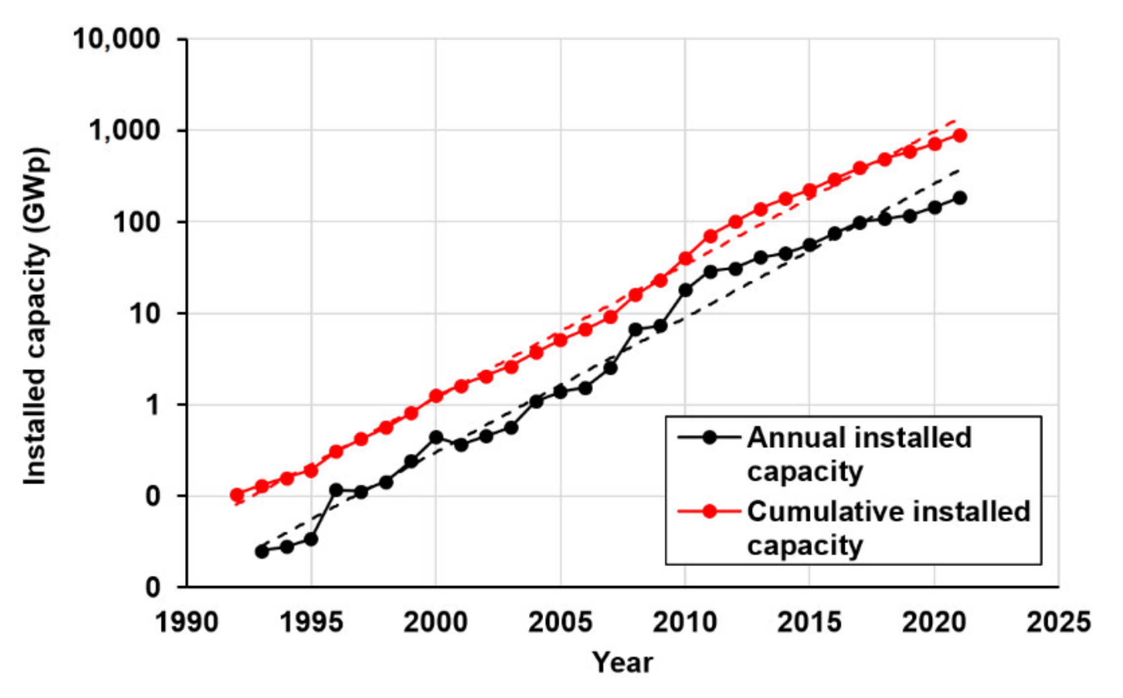
Over the past 20 years advances in technology have led to an impressive reduction in the cost of photovoltaic modules and other components, increasing efficiency and significantly improving both the reliability and the yield of the system, resulting in reduced electricity prices. These advances are associated with the rapid growth in the installed capacity of photovoltaic power plants. Photovoltaics has become one of the world’s fastest growing energy segments. The cumulative PV capacity installed worldwide exceeded 760 GW
p in 2020 [
1], of which over 140 GW
p was installed in 2020. The developments of the cumulative capacity and annual production in period 1992–2021 [
2,
3] are shown in
Figure 1. As shown, the cumulative installed capacity increased a thousand-fold between 2000 and 2020. In 2021, annual production (installed capacity) increased to more than 160 GW
p and in 2022 a further increase in annual production is expected. In this way, in 2022, the cumulative PV capacity installed worldwide would exceed the TW
p level.
A very important part of photovoltaic systems are photovoltaic modules, which convert solar radiation into electricity. Their price, efficiency, and durability are important drivers for the development of photovoltaics as a future source of cheap and clean electricity. This paper discusses the influence of price, efficiency, and service life of PV modules on the levelized cost of energy (LCOE) (along with the availability of materials); the resulting trends in PV module technology; and some limits for the relevant technologies.
2. Drivers of Photovoltaic Technologies
The price of electricity produced by a system (e.g., photovoltaic systems) is usually determined by a system LCOE analysis that allows different production methods to be compared [
4,
5,
6]. The LCOE represents the total cost of a system (brought back to present value) divided by the total amount of energy produced during the system service life. Considering inflation and discount factors, LCOE equations can be complicated.
If the system service life is n years, the price of energy can be expressed in simplified form as the sum of the total cost of acquisition and operation of the system (investment costs ICk, including interest and inflation in individual years and operating costs OCk in the kth year of operation) and the energy EPk produced in the kth year of operation.
Since photovoltaic systems are normally commissioned and installed in much less than a year, the LCOE can be expressed in a simpler form
where
IC is the total purchase price,
OCAV is the average annual operating cost,
n is the service life of the system (in years), and
EP is the total energy produced by the equipment over its service life.
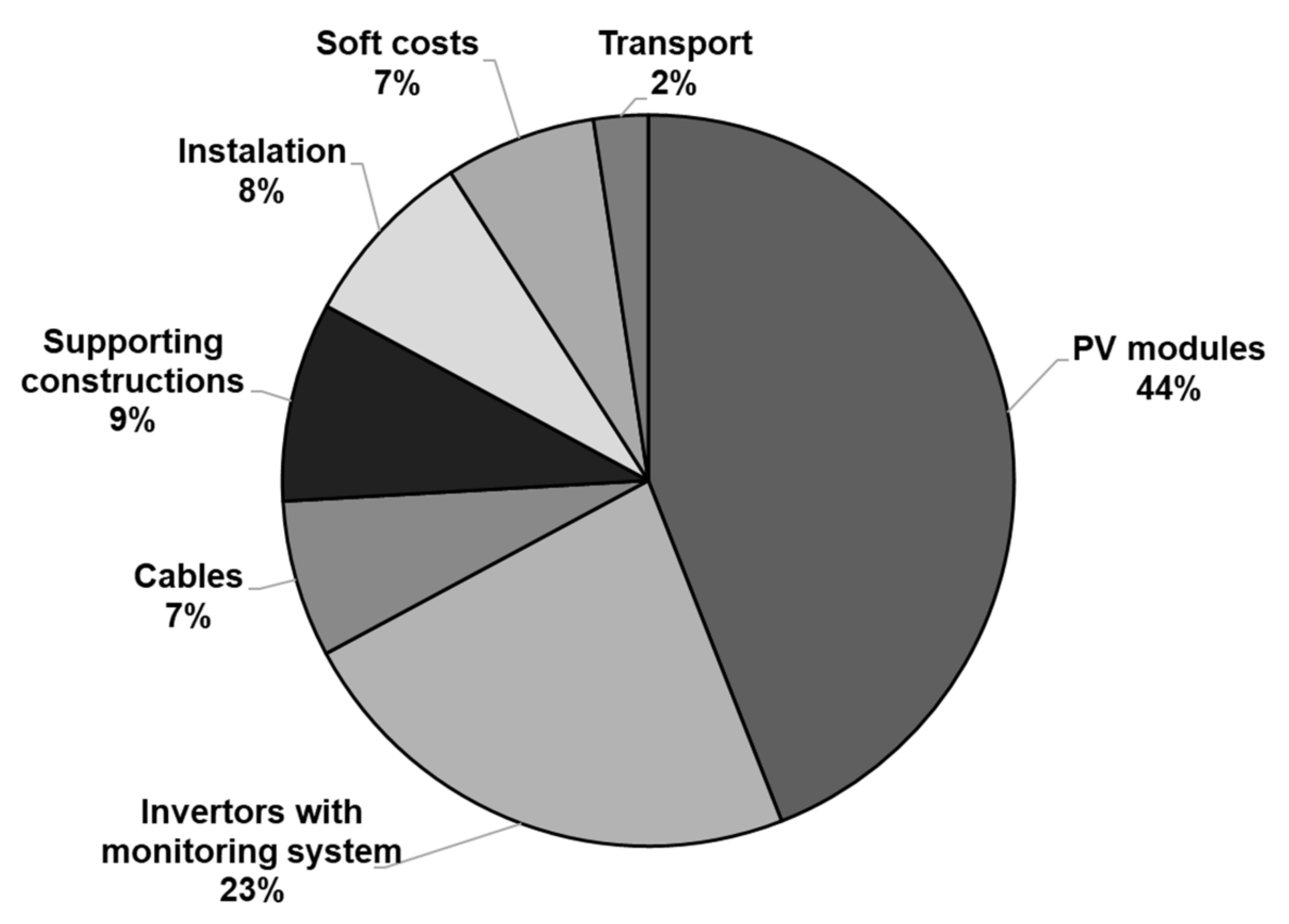
Different categories can be used for investment cost analyses. Usually, system costs are divided into module costs and balance of system components (BOS) costs (this division is historical from the times when module costs were the largest part of system costs). System components’ market prices are relatively stable. However, in addition to these costs, there are also so-called soft costs, which represent costs associated with the project, land, administration, margins, taxes, financing, etc., which may vary depending on the type of installation and the installation location. As reported in [
5], soft costs may represent from 20% to 60% of the total investment costs. When systems are installed on the roofs of buildings, these costs usually do not include the land costs (or the lease costs), so the soft costs are then limited significantly. A typical division of the costs of a 500 kW
p commercial roof system within the Czech Republic is shown in
Figure 2.
For a commercial roof system, the installation cost can be written as
where
MC is the module cost,
BC is the BOS cost (including cable, construction, transport, installation, and inverter costs) and
SC represents the soft costs. With respect to the module parameters—the module output power and module efficiency, both at standard testing conditions (STC), module size, module weight, etc.—and the warranties for the module parameters, it is useful for further analysis to use a different non-module cost structure [
6].
Module cost is defined as the cost of unit power (measured under STC), usually counted in USD/W
p. The cost of some BOS components is associated with the power of the unit (inverters, transformers, switchboards, etc.); the cost of another BOS component is associated with the area requirement per unit of power (i.e., the required area of the supporting structures, the length of cabling, etc.). Part of the BOS cost is, therefore, inversely proportional to the efficiency of the module. Accordingly, the use of less efficient (albeit cheaper) modules may not reduce investment costs [
7]. From that observation, it follows that the three most important drivers of photovoltaic technology are PV module cost, PV module efficiency, and PV module service time.
2.1. PV Module Efficiency
In addition, soft costs can be divided into parts: a part proportional to the PV system area, a part proportional to the system power, and a part that is fixed. In this way, the non-module costs can be divided into “area-related” costs,
A, and “others,”
O. Then, the investment costs,
IC, as a function of the module efficiency,
η, can be expressed as:
where
M is the module costs,
A is the area-related costs, and
O represents the others.
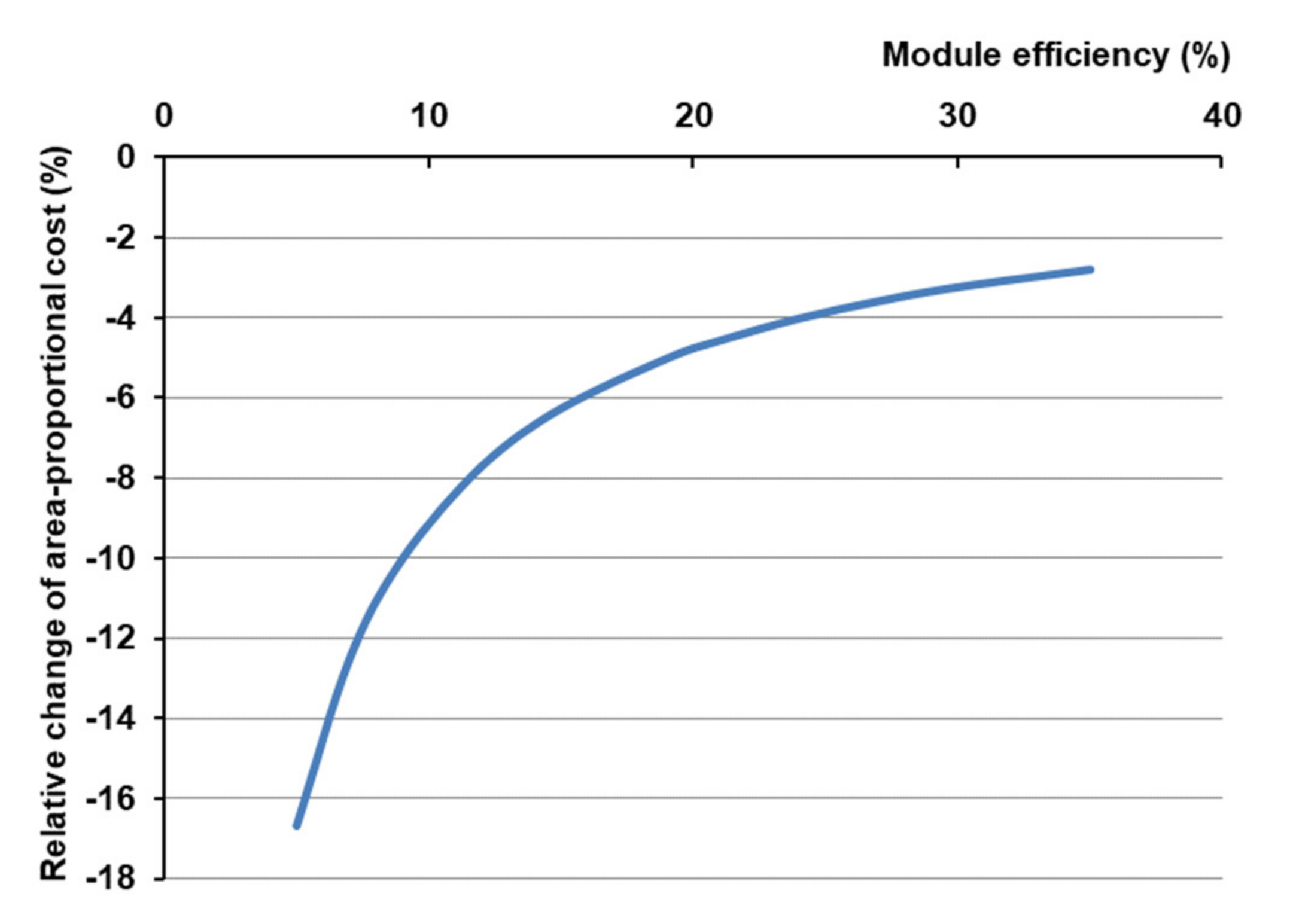
If
D is a coefficient of proportionality, the area-related costs can be expressed as:
With a change in the module efficiency from
η1 to
η2, the relative change of the area-related costs is
However, as the efficiency of the modules increases, the relative change in the area-related costs decreases, as shown in
Figure 3, where the relative changes of the area-related costs caused by a 1% increase in module efficiency are plotted as a function of module efficiency. For example, an increase in efficiency from 10% to 11% results in a relative reduction in the area-related costs of 9%; an increase in efficiency from 20% to 21% leads to a relative reduction in the area-related costs of 4.8%. The overall reduction in total investment costs due to the increase in module efficiency will be proportional to the share of the area-related costs in the total investment costs. In the latter case, in a system with approximately 33% area-related costs, there will be a relative decrease in total investment costs of 1.6%.
Besides improving module efficiency, the use of higher system voltages (e.g., 1500 V), sun-tracking constructions, or bifacial modules can result in system-level changes in the expenditure structure [
7]. Increasing module power can also help reduce BOS costs [
8] by reducing the spending on other components, including racking, foundations, and cabling.
2.2. PV Module Costs
Module costs are usually based on market prices and quoted as price per unit of power, measured under STC. They may be quoted in USD/W
p, or EUR/W
p. The price of a module may vary in different countries, due to the tax systems, the costs of transport and the volume of deliveries, the margins of resellers, etc. Differences in prices in different countries can be significant. For example, compared to module prices in Germany, module prices are 17% higher in Australia, 52% higher in the USA, and 60% higher in Japan [
9].
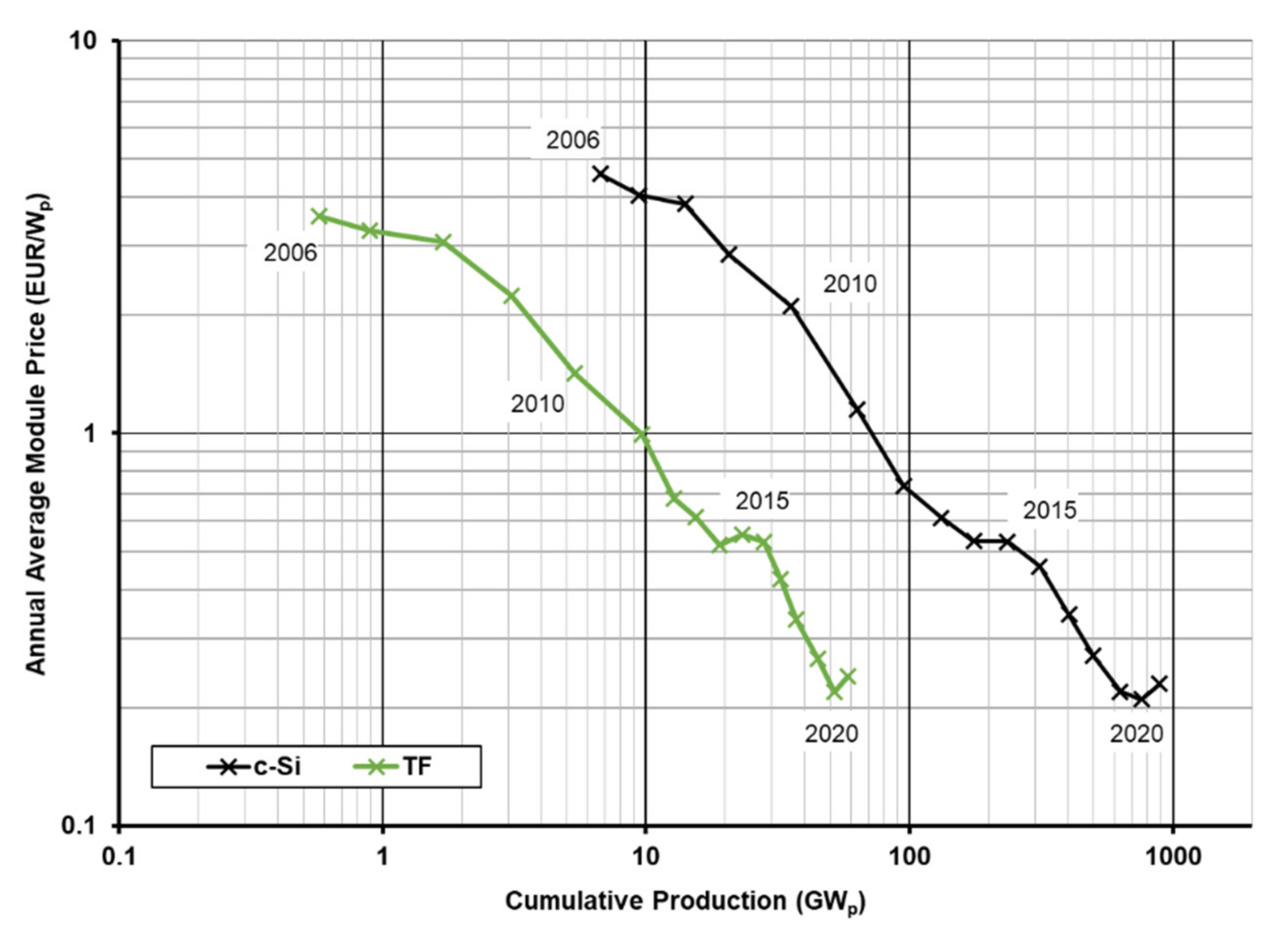
As cumulative production levels have increased, module costs have decreased, as shown in
Figure 4 for crystalline silicon (c-Si) and thin-film modules (TF). Experience with the technology has resulted in improved yields, more efficient use of raw materials, and reduced labour costs. There have been step-changes through technological breakthroughs, the expansion of the production plants, and the use of increased automation. In addition, the costs of materials, components, and energy used in the production chain are important factors.
A technological learning in PV modules [
10] is demonstrated in
Figure 4.
2.3. Influence of Efficiency on Module Costs
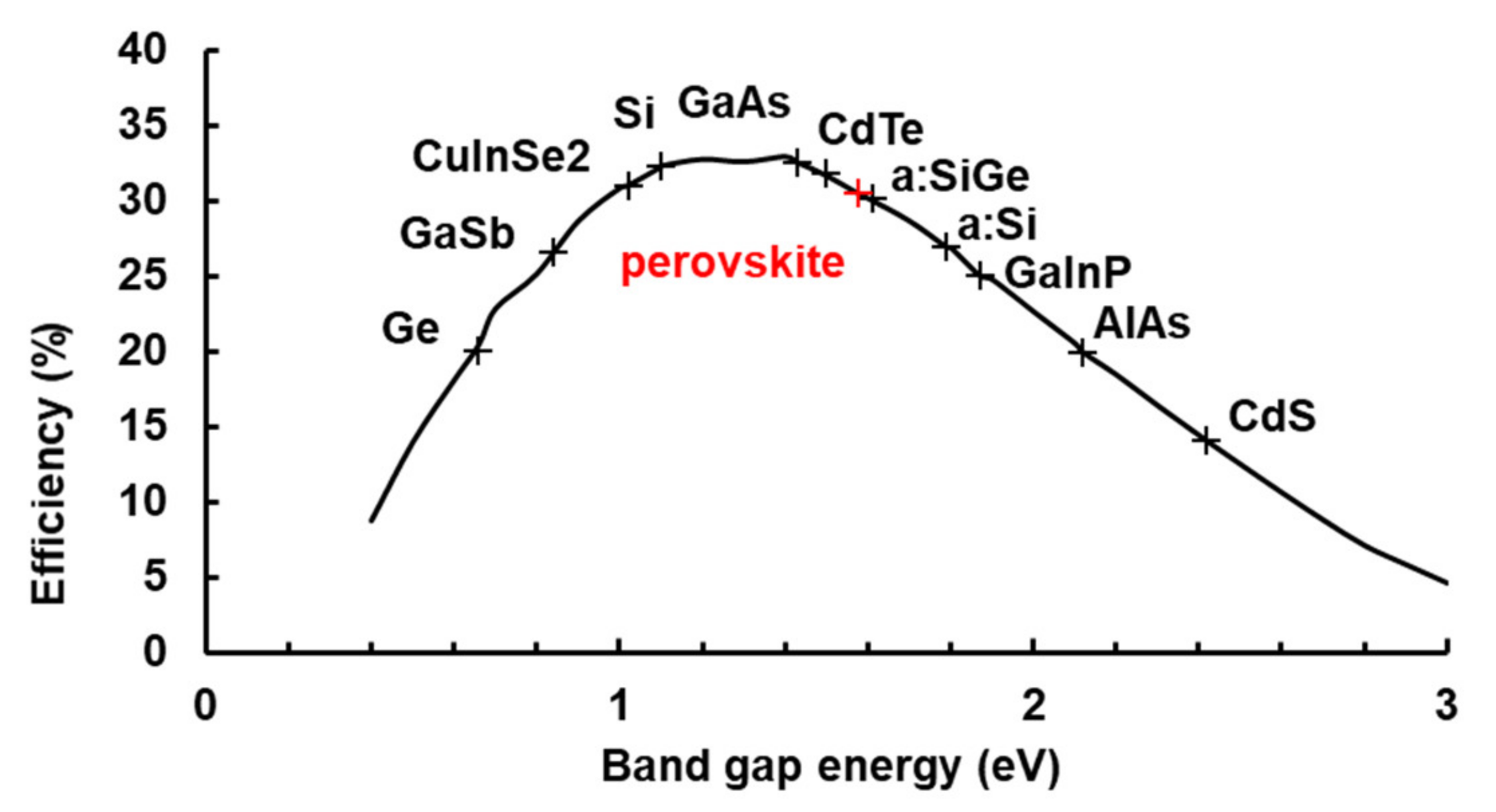
The maximum theoretical efficiency of a PV cell,
ηuc, depends on the irradiation spectrum and the absorbing materials. For a cell with a single absorbing material, irradiated with the standard AM 1.5 spectral distribution, the maximum theoretical efficiency varies with the material band gap, as shown in
Figure 5 (only radiative recombination is considered). If Auger recombination is also considered, the maximum theoretical efficiency for monocrystalline silicon is 29.4% [
11].
The actual efficiency of PV modules will always be lower than that of their cells, and their efficiency will be lower than the theoretical maximum. Modern design principles and technologies make it possible to reduce many of the optical and ohmic losses associated with the module array, but the ultimate module efficiency remains less than the theoretical maximum: ηum ≤ ηth. However, the materials and procedures needed for the module efficiency, η, to approach ηum increase the production costs, so that the module cost, M(η), increases rapidly.
This trend can be modelled as
η < ηum, as shown in Equation (6):
where
B,
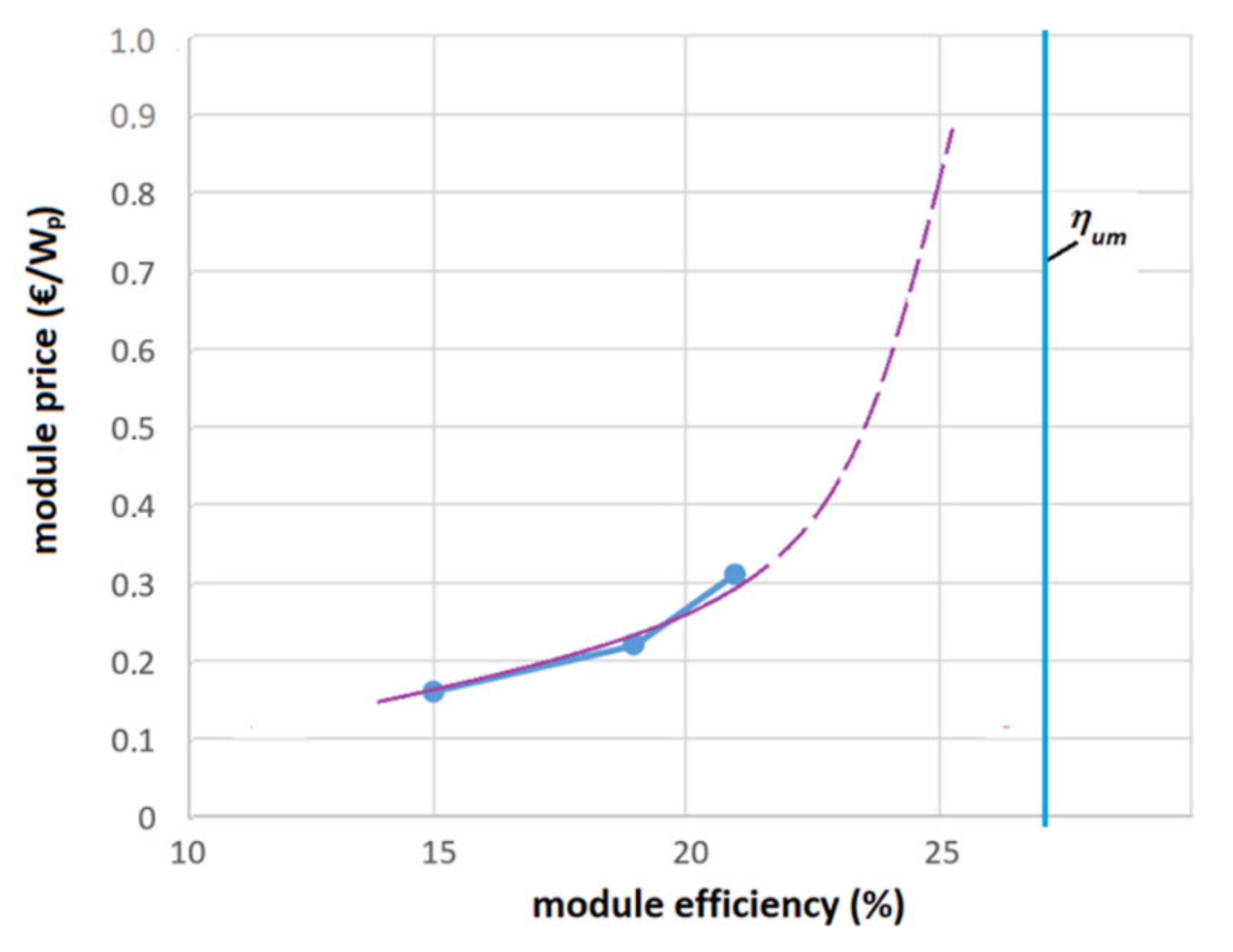
C, and
a depend on materials and the technology level. Such a trend can be found in current module prices [
12] if an efficiency of 15% is associated with a “low price,” an efficiency of 19% is associated with a “mainstream price,” and an efficiency of 21% is associated with a “high price” module category, as indicated in
Figure 6.
In this approximation, the dependence of the investment cost
IC on the module efficiency would be expressed by
which can be used to find the optimal solution (as a case study based on detail knowledge of costs structure in the locality). With progress in manufacturing technologies, the optimum efficiency moves to higher levels.
2.4. PV System Operating Costs
Systematic maintenance is very important for the reliable operation of photovoltaic systems. Such maintenance includes regular inspection and preventive maintenance activities, stand maintenance, module cleaning, snow clearing, etc., and corrective maintenance (cabling repairs, exchange of defect PV modules, inverters, and other components). Regular monitoring and diagnostics of the system allows minimizing losses in case of failures. These activities are carried out either by an entity’s own employees or with the help of specialized service companies.
In addition to maintenance, monitoring, and repair costs, there are other costs, such as administrative costs, property taxes, insurance, land leases, grid fees, balancing, asset management, security, various taxes, and other costs due to inflation, expiring warranties, etc. [
13,
14]. The operating costs are the sum of both maintenance and additional costs. Like the investment costs, a part the operating costs is area-dependent.
There are differences in the operating costs of a PV system due to differences in system size, system configuration, climate, and location. There can also be big differences in individual years of operation. These differences complicate the determination of average operating costs. A system tool for calculating operating costs can be found in [
15]. The average operating costs are usually stated in cost per kW
p of installed power.
2.5. The Influence of Module Service Life
When evaluating the service life of a PV system, it is important to consider the system as a whole. The installed PV system can only provide the expected service life if all of its components work properly and the entire PV system is properly serviced, from the PV modules to the high voltage connection.
In the case of PV modules, the influence of the environment gradually reduces the efficiency, while the other components may show a fault that affects the function of a part of the system and can be repaired. Repairs can be included in operating costs, losses associated with failures (and thus with non-energy production), reducing the efficiency of the system.
From this point of view, it is possible to approximate the service life of the PV system to the performance guarantee period of the PV modules specified by the manufacturer (only 2% of PV modules are predicted not to meet the manufacturer’s warranty after 11-12 years of operation [
16] and project life expectations are now even higher than 30 years [
17]). This projection of service life is also made possible by the fact that the currently stated service life of inverters is gradually approaching the service life of the modules [
18].
The PV system service time, n, also has some influence on the LCOE of photovoltaic systems.
In a simple approximation [
19], the LCOE can be expressed by
where
and
EP1 is the energy produced in the first year of production.
Expecting an average irradiance for all years, it is possible to use the following equation as a good approximation:
where
YR is reference yield,
PSTC is nominal power of PV field,
ξ(T;
G) is operating condition factor, and
ηc is DC-AC conversion efficiency.
If we assume only the effect of the change in the service life (and other parameters do not change), the relative change in the LCOE when changing the service life from
n1 to
n2 years can be expressed by
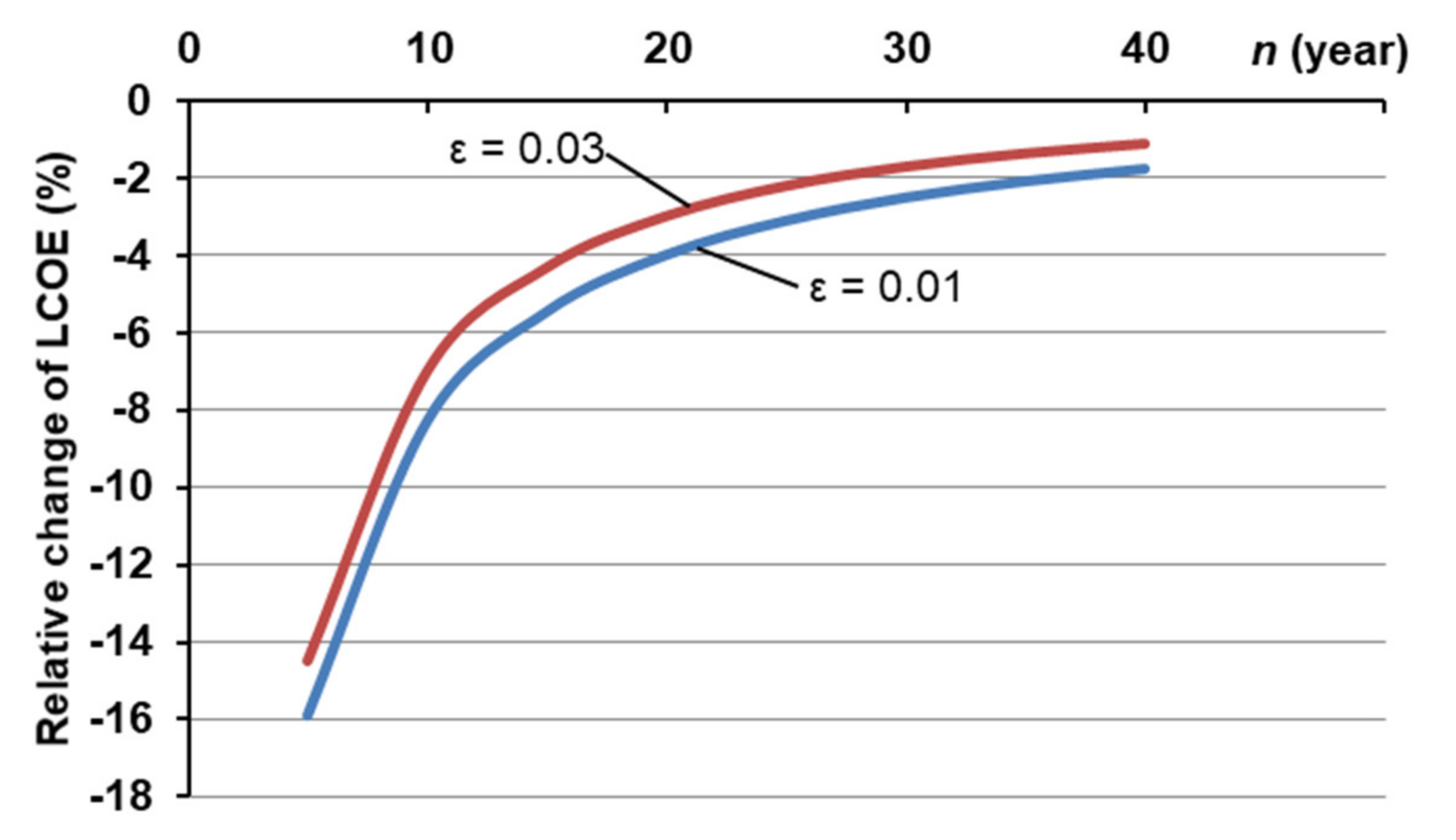
Using this approximation, it is relatively easy to quantify advantages following from the module service time prolongation. With a constant investment cost and energy output, the module service life prolongation results in a decrease of the LCOE.
In
Figure 7, the relative changes of the LCOE caused by an increase in the module service life of 1 year (from
n to
n + 1) are plotted as a function of module service life
n (e.g., an increase in the service life from 10 to 11 years results in a relative reduction in the LCOE of 8.26%; an increase in the service life from 20 to 21 years leads to a relative reduction in the LCOE of 3.94%). Comparing
Figure 2 and
Figure 6, it can be stated that the effect of module life extension on the LCOE is comparable to the effect of increasing the efficiency of modules.
When assessing the service life of a PV system, it is important to consider not only the PV module but the system as a whole, from the solar cell to the high-voltage connection. In addition to the influence of module degradation, described by the expected decrease of module efficiency, there may be defects in both modules and other parts of installation, causing random failures in the PV system’s operation. Repairing these failures increases the operating costs of the system, resulting in an increase of
ε that is followed by a decrease of the relative reduction in the LCOE, as demonstrated in
Figure 7. It should also be considered that during a fault, the system operates at reduced power, thus reducing the DC-AC conversion efficiency.
Another important criterion for the development of photovoltaic technologies is a sufficient source of materials. All materials in the technology chain should be generally available so that their absence does not limit future development.
3. Present PV Technologies
The criteria of low cost, high efficiency, long service life, and availability of raw materials are currently best met by crystalline silicon modules. There are In, Te, and Se source limits for CdS/CdTe and CIGS thin film modules. For both CdTe and CIGS modules, the maximum production limit was set at 20 GW
p per year [
20], which is well below the expected future demand of several hundred GW
p per year. Amorphous silicon modules have low efficiency and other technologies have not yet reached the required service life level [
19].
During technological development since 1970, there have been several important changes in the design and technology of crystalline silicon cells and modules (four generations of crystalline silicon cell technology were considered in [
21], depending on the complexity of the technological process).
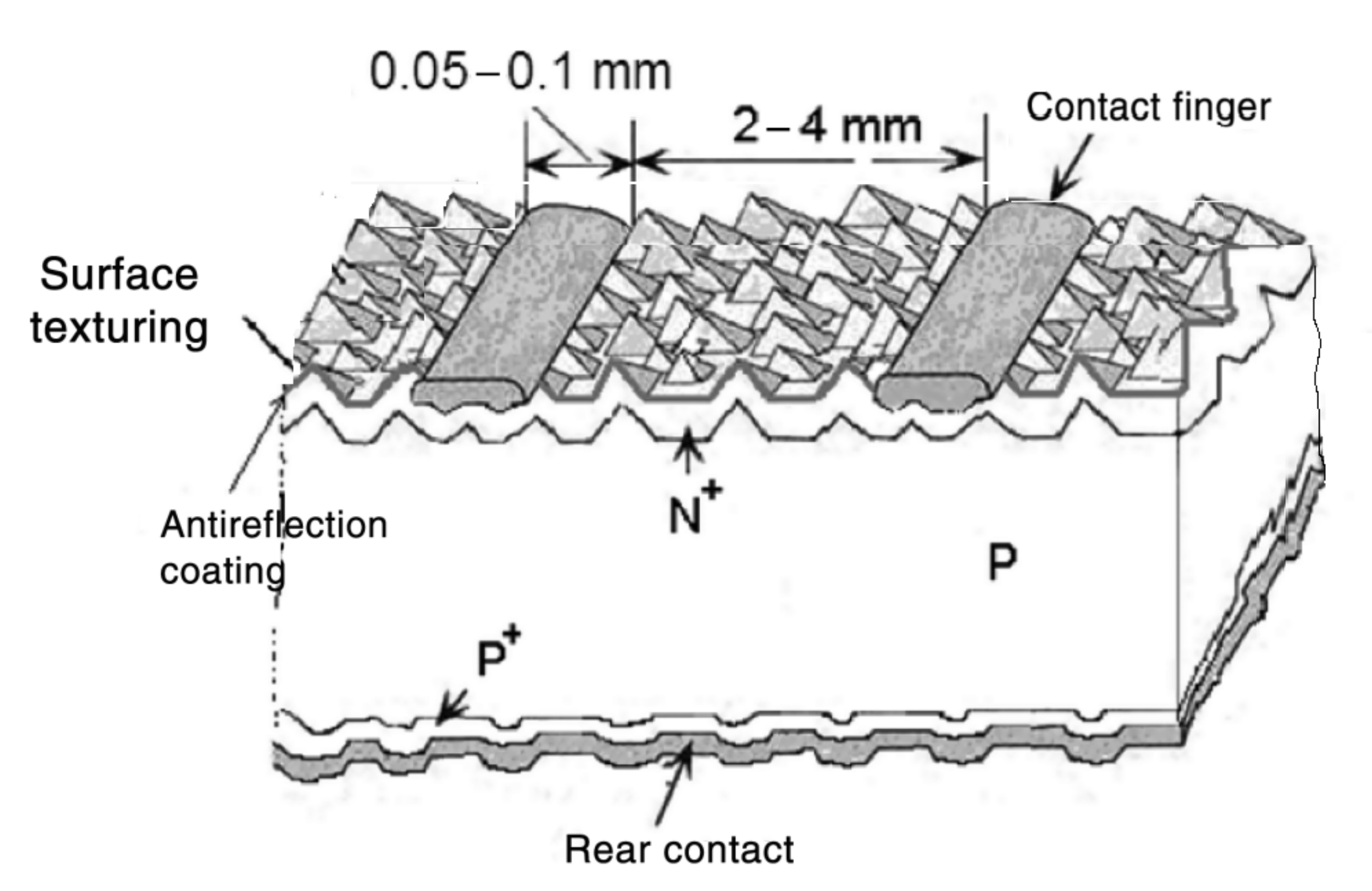
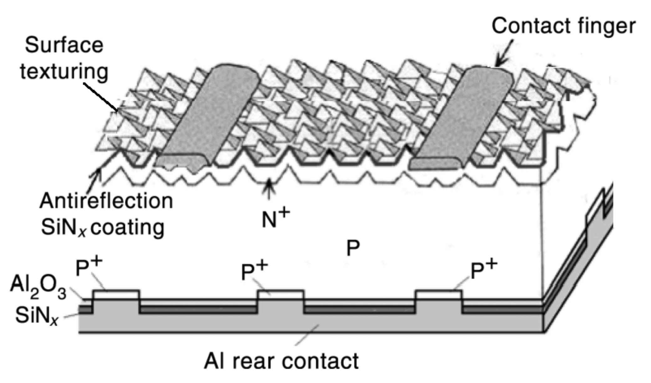
During their development in the 1980s, back surface field (BSF) technology was introduced into mass production, enabling the production of cells from a P-type starting material without costly photolithography and vacuum deposition. The standard cell structure (BSF) is shown in
Figure 8. BSF technology solved the problem of front surface reflexivity by combining the application of surface texture and an anti-reflective layer with the back contact low resistance of the PP
+-metal structure realized by the Si-Al alloy deposition process. No technological step requires a process temperature higher than 900 °C, which has made it possible to produce cells with acceptable efficiency even from multicrystalline wafers. The boron-doped P-type starting material was used in accordance with the easier production of crystalline rods with a uniform resistivity distribution due to the high boron segregation coefficient.
However, during crystalline silicon fabrication, the molten silicon is kept in a quartz crucible, from which a certain amount of oxygen is incorporated in the crystalline silicon. This is a disadvantage, as oxygen forms B-O complexes, which can act as recombination centres and reduce the carrier’s lifetime. It was found that the defect concentration is directly proportional to the boron concentration and squared to the interstitial oxygen concentration [
22].
During this development, there were many improvements in the structure and technology of cells (optimization of impurity concentration, contact configuration, passivation of grain boundaries, optimization of the anti-reflective coating, reduction of wafer thickness, etc.), leading to increased efficiency and production costs. In the period 2008-2016, the share of starting multicrystalline material increased to 66%, but thereafter it quickly decreased below 20% in 2020 [
23].
3.1. PERC PV Cell Technology
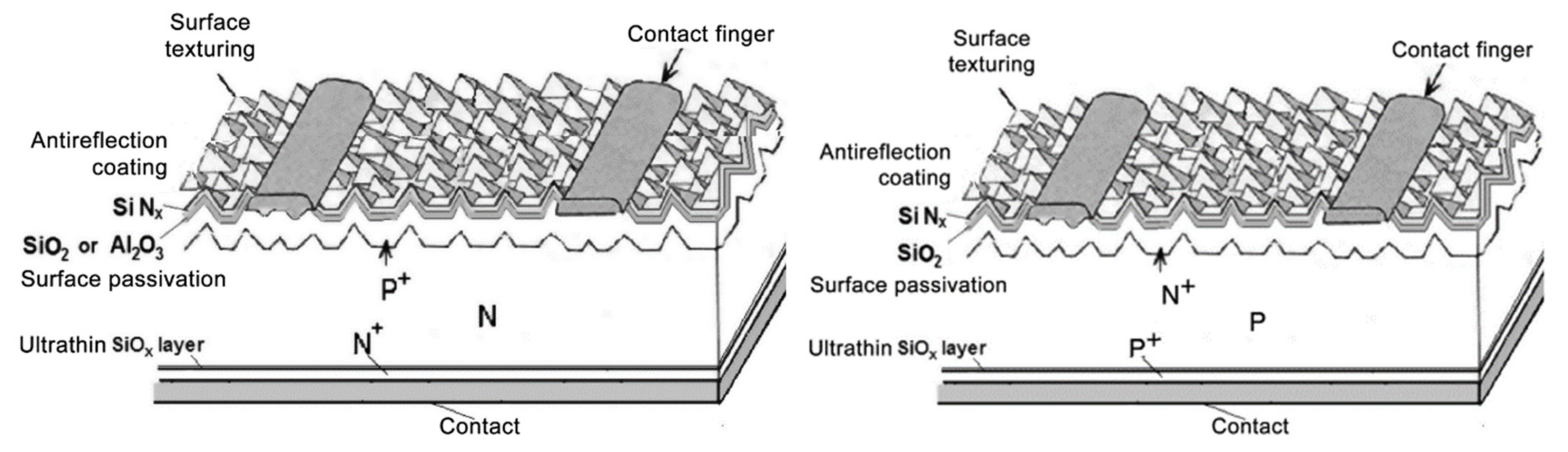
The increase in the efficiency of BSF cells is limited by both volume recombination and the relatively high recombination rate at the PP
+ contact. To reduce recombination in volume, it was necessary to switch to monocrystalline material. The problem of surface recombination could be solved (after finding a productive and cheap technology) using the passivated emitter rear contact (PERC) structure, as demonstrated in
Figure 9. The solution is covering a significant part of the back surface with a dielectric film containing positive charges, thereby electrically passivating it. The contact of the back of the cell is made through a series of holes (with fixed distances and diameters) whose total area is only about 1–4% of the total area of the PV cell. PERC cells with 23% efficiency [
24] were demonstrated as early as 1989, but the technology used was too expensive at the time to be accepted into series production.
After 2010, the development of Al2O3 passivation layer deposition and the realization of the contact hole pattern by local laser ablation decreased the technology cost increment connected with three additional technological steps (rear surface etching, passivating Al2O3 layer combined with SiNx:H layer deposition, and local windows opening by laser ablation) to an acceptable level.
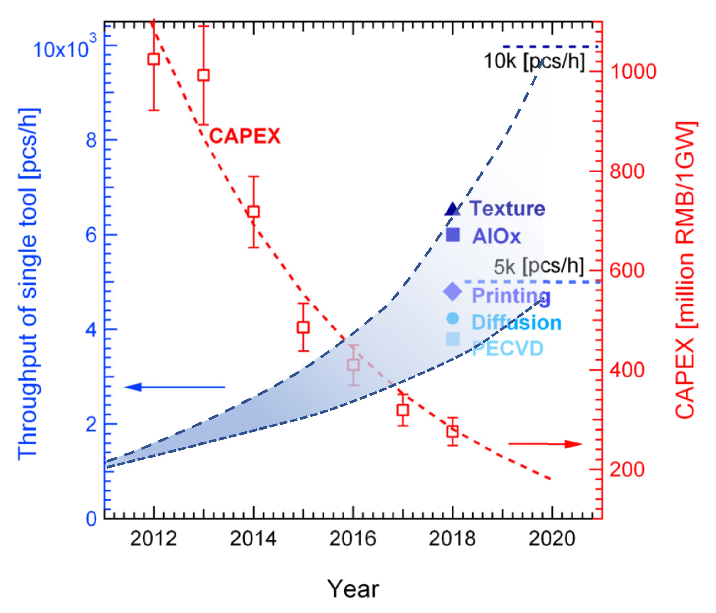
The development of production equipment, increasing throughput and decreasing PERC workshop investment costs [
25], as demonstrated in
Figure 10, accelerated the transition from BSF to PERC technology. While in 2015 the PERC technology share was less than 10% [
26], in the year 2020 it represented more than 80% [
27].
As already mentioned, one of limiting factors for PV cells from P-type starting material was forming B-O complexes (LID), decreasing the PV cell’s efficiency. The ways to eliminate this effect are either the reduction of the interstitial oxygen content or the substitution of the boron by a different dopant. Fabricating industrial boron-doped Cz silicon or Fz silicon with low oxygen content (<3 ppm) is very difficult and expensive. Attention was focused on using gallium as an acceptor [
28]. The difficulty of applying gallium-doped silicon wafers lies in the control of the resistivity in the ingot [
29], because there is a significant difference between the segregation coefficient of boron (0.75) and gallium (0.008). With process optimization at the ingot pulling, it has been possible to deliver Ga-doped wafers at similar prices to B doped wafers and PV cells made with Ga-doped wafers demonstrated an efficiency improvement [
30]. The process of replacing boron doping with gallium doping was very fast. It started in 2018; in 2019, 10% of P-type monocrystalline wafers produced were gallium-doped [
31]; and in 2020, 60% of P-type monocrystalline wafers produced were gallium-doped [
27]. Gallium-doped monocrystalline wafers have become mainstream.
Introduction of a selective emitter process in low-cost production, the reduction of contact resistance for weakly phosphorus-doped silicon, the reduction of front metallization finger widths from approximately 100 µm to less than 30 µm in large-scale production, and contact grid optimization were important steps in achieving the current high-efficiency PV cells in bulk production. The latest comers in silicon PV manufacturing benefit from cheaper production tools with higher productivity: larger cells (from 125 mm square P-type wafers in 2010 to 182 mm or even 210 mm in 2021), thinner wafers, less kerf-loss in slicing, more wafers per batch in operations, higher technology tool throughput, and more automation increasing labour productivity [
27,
32].
3.2. Higher Efficiency PV Cell Technologies
Although in N-type silicon the bipolar diffusion coefficient is three times smaller than in P-type, the lifetime of N-type silicon carriers is in the order of milliseconds (i.e., an order of magnitude higher than in boron-doped P-type Si), and longer diffusion lengths can be achieved [
33]. For this reason, N-type monocrystalline wafers are suitable as a starting material for high-efficiency solar cells.
N-type-based crystalline silicon technologies—interdigitated back contact (IBC), heterojunction technology (HJT), and tunnel oxide passivated contact (TOPCon)—have higher efficiencies (23–25%) and a lower temperature coefficient in comparison with boron-doped P-type-based technologies [
33,
34]. However, their market share remains relatively low (5% in 2015, 5% in 2019, and 5% in 2020), probably due to the higher costs of fabrication [
35] (especially in the case of IBC and HJT) and consequently, they come with a higher price. The progress of industrialization is impacted by numerous factors, including the improvement in efficiency, the progress in cost reduction, and the initial investment in production lines, where the key lies in the follow-up on cost reduction for primary segments. However, an increase in the market share of N-type-based crystalline silicon technologies is expected in the future [
27], especially in applications with higher area-dependent costs. Prospective developments in N-type PV cell technologies are discussed in [
36,
37,
38].
Advances in gallium doping make it possible to produce a P-type starting material with a carrier lifetime comparable to that of the N-type. These advances make it possible to produce highly efficient cells from both types of materials. For PERC cells, efficiency is limited by the series resistance associated with current contraction into small area contacts. The TOPCon structure solves this problem by means of a 1–2 nm thick SiO2 layer, which allows the tunnelling of major carriers into a several hundred nm thick layer of heavily doped microcrystalline silicon, provided with full-area contact. The front side of TOPCon cells is designed in the same way as the PERC structure, so the investment requirements for the transition from PERC to TOPCon are not very high.
The TOPCon structure is shown in
Figure 11. The theoretical efficiency limit for TOPCon cells is about 28% [
39]. For the N-type starting material, 25.21% efficiency was reached; for P-type starting material, 25.19 % efficiency was reached [
40].
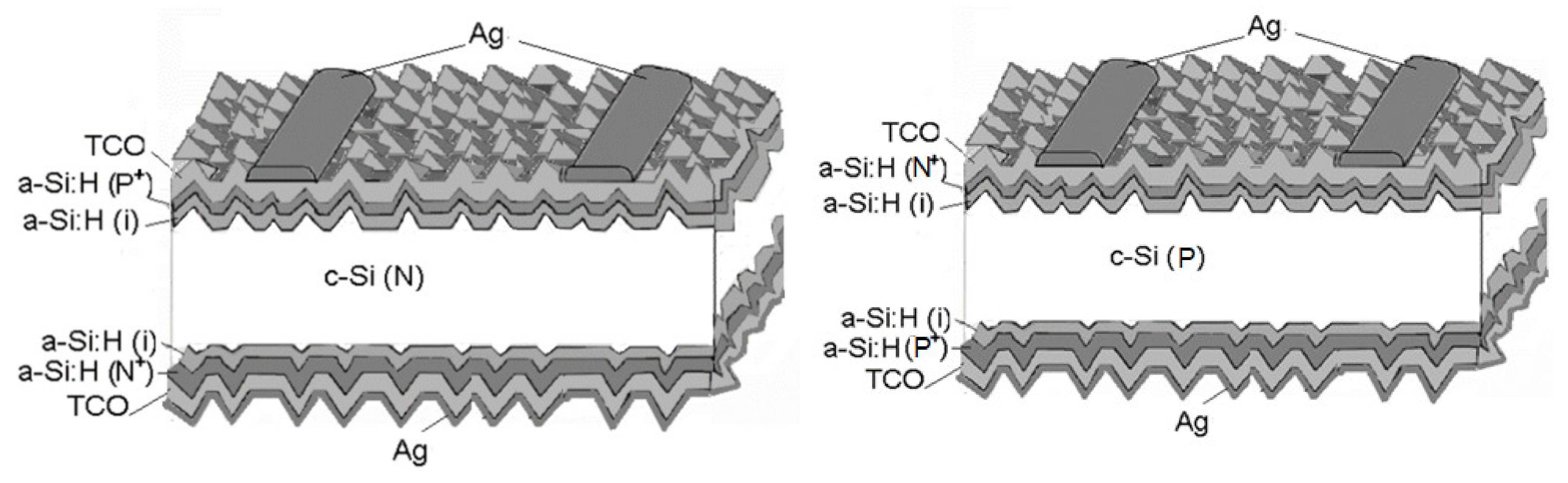
High-efficient cells can be obtained also using heterojunction technology (HJT). Cells on the base of the heterojunction, between the amorphous and c-Si, utilize very thin (10–20 nm) a-Si:H layer stacks of N-type (or P-type) wafers to provide surface passivation, emitter formation, and a back surface field [
41,
42], as demonstrated in
Figure 12. The a-Si:H layers are deposited on c-Si by PECVD using a low-temperature process (below 200 °C). On both doped layers, transparent conductive oxide layers are formed by sputtering, and metal fingers are screen printed. However, the a-Si:H layers cannot be exposed to a temperature above 200 °C, thus special low-temperature curing pastes are required.
PV cells have the ability to capture light from both sides and thus to increase the excessive generation of carriers and the subsequently generated current, if the electrical contacts are designed accordingly. Such cells can collect diffuse radiation and radiation reflected from the surroundings (albedo) by the back surface, thus increasing the overall efficiency. An example of a simple bifacial cell structure is shown in
Figure 13. It is necessary to ensure that the passivation dielectric layer on the rear also acts as an anti-reflective layer. In 2020, bifacial cells represented about 30% of total production [
27] and this share is expected to grow significantly in following years [
43]. Bifacial cells can be realized using PERC, TOPCon, and HJT technologies.
3.3. The Module Assembly Technologies
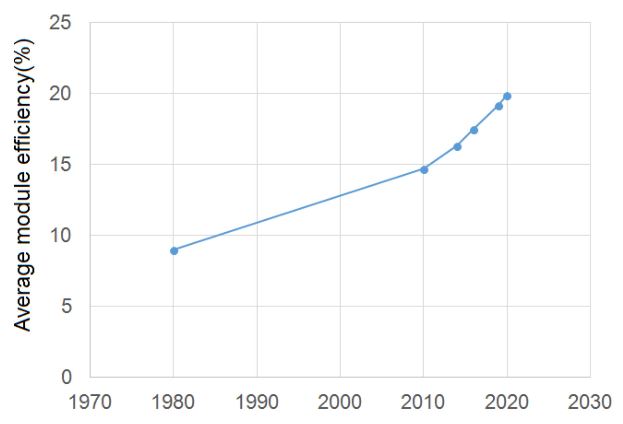
The modules are assembled from cells of almost the same parameters and the efficiency of the module is lower than the efficiency of the cells from which it is assembled. Cell-to-module (CTM) losses are due to the reflectivity of the outer protective layer, the absorption of light in the encapsulating layers, unabsorbed radiation, ohmic losses at the connections of the cells into strings, etc. [
44]. The present module design and technology can be improved through improving light management (e.g., reducing the reflectivity of the glass by means of antireflective coatings, optimization of cell spacing, increasing the reflectance of internal inactive areas, and reducing the optical shadowing of metal) and reducing resistance losses (e.g., increasing number of busbars, using half-cut cells or strip cells for shingling, optimizing ribbon cross-section according to the width, optimizing junction box and cabling design). By combining these tools, CTM losses can be reduced below 2%. In combination with the PV cells’ efficiency improvements, the PV module efficiency increases, as shown in
Figure 14 for average c-Si module efficiency. The top module efficiency has reached 23% [
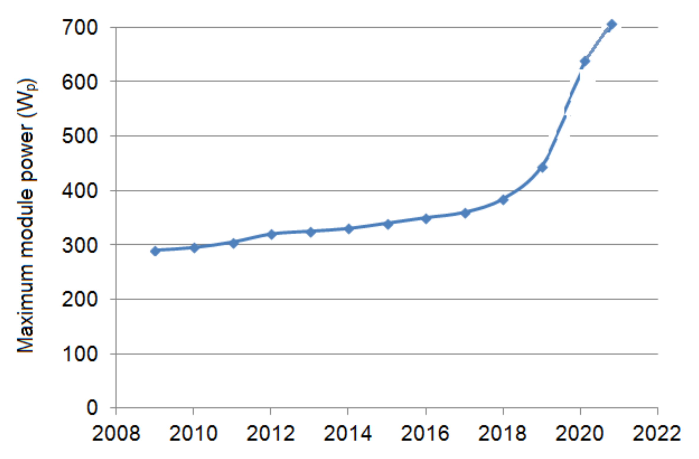
45] using P-type PERC cells. Another trend stems from the ability to produce larger solar cells. The larger cell area allows the production of large area modules with high power that help reduce BOS costs [
46]. The increase in maximum module power is shown in
Figure 15. However, increasing the area of the module places greater demands on handling and on the resistance of the modules to mechanical stress.
3.4. PV Module Service Life
PV modules are designed for outdoor use and are therefore subject to weather, climate, and many other factors. Damage to modules in operation is frequent and can affect different parts of the modules. UV exposure alters the polymers used to encapsulate the photovoltaic cells and modifies the mechanical and optical characteristics of these polymers. Moisture can penetrate the module and degrade welds, cables, and connections. Freezing can cause mechanical stress, while in the desert, sand can erode materials, etc. Stressors (sunlight, humidity, wind, snow, rain, hail, high/low temperatures, temperature changes, salt, sand, dust, etc.) interact with several factors, such as module materials, cell technology, encapsulation materials, etc.) All stress factors are singular stress parameters, but often they are present and active in different combinations. These combinations have a higher damage potential than the sum of the individual parameters [
47]. Module durability is affected by the design, the module production process, the quality control procedures, the DC voltage between the module frame and the cells, the module assembly system, and, finally, the operational maintenance [
48].
Of the components of PV modules, the encapsulants are the most susceptible to aging; therefore, most prominent PV module failure mechanisms are linked to the used polymeric encapsulation materials [
49,
50]. In addition, interactions with other module components, such as ribbons or cell metallization, can result in unexpected degradation mechanisms or failure modes [
51]. Detailed understanding of the degradation processes of photovoltaic modules and materials is a prerequisite for the successful development of new components and constructions, and for the fabrication of photovoltaic modules.
As indicated in
Section 2.3, the module service life is one of important drivers of PV technology, as prolongation of the PV module service life has a similar effect as that of increasing the module’s efficiency. The present service life of c-Si modules is usually declared to be 25 years (or more). For example, bifacial modules with double-sided glass, with polyolefin (POE) encapsulation, have a service life of well over 30 years.
One of the problems is that the present modules use materials and technologies that did not exist 25 years ago, and the reliability of new PV module designs cannot be proven with field data. Therefore, the data of new module types are obtained using accelerated testing, usually utilizing some international standards, which changed significantly after the solar boom in 2008. These standards gradually consider the phenomena that appear during real operation, to avoid their negative impact on future modules and to give the operator a guarantee of quality. For example, the potential induced degradation effect, which was unknown in 2008, was described and implemented in special international standard IEC TS 62804-1:2015 and, since February 2021, it has been implemented in the basic PV standard IEC 61215-2:2021 (the original standard is still valid, but it can be predicted that it will be withdrawn soon). Due to changes in PV module structure (different encapsulation materials, lower thickness of glass, etc.), cycling (dynamic) mechanical load testing, bifacial modules testing, and special procedures for flexible modules were implemented.
The same situation applies to the other effects and technologies. Because the development of new PV technologies is unpredictable, the previously used two standards (IEC 61215 for crystalline and IEC 61646 for thin film modules) were joined into one standard IEC 61215-1-X, whose structure allows new technologies to be added quickly. The standard procedures for testing are the same and only deviations relevant for concrete technologies apply. The “X” in these standards designates concrete technology. When a new phenomenon or material requires serious evaluation, standards in the form of “technical specification” are usually used (for example IEC TS 60904-1-2:2019 for bifacial modules, IEC TS 60904-13 for electroluminescence testing, or IEC TS 62788-7-2:2017 for accelerated weathering tests of polymeric materials).
4. Technology Roadmap and Limits
The development of photovoltaics in coming years will be associated with a continuing shift to the production of PV modules with higher efficiency and durability, while maintaining (or reducing) the price. Crystalline silicon modules will remain the mainstay of technology. In terms of efficiency and price, thin-film modules can compete with them, and intensive development and research is occurring in the field of perovskite technologies.
In the family of new technologies, the most promising are hybrid organic–inorganic metal halide perovskites. Due to their high efficiency (above 25% on laboratory cell samples [
52]) and low manufacturing costs, perovskite solar cells have a great potential to become one of the leading technologies in the PV industry. Recently, perovskite structures approached pilot line production for both flexible modular roll-to-roll lines [
53] and silicon-perovskite tandem lines [
54,
55,
56]. A serious problem of perovskite structures was low stability, which has improved significantly, but certain problems persist and hinder the development of this technology, and the service life in field conditions is still not fully satisfactory. Therefore, improving the quality and stability of perovskite modules is still the subject of intensive research and development [
57,
58,
59,
60,
61,
62]. In addition to the problem of perovskite stability, technology needs to be improved to achieve technological sophistication in large-scale production.
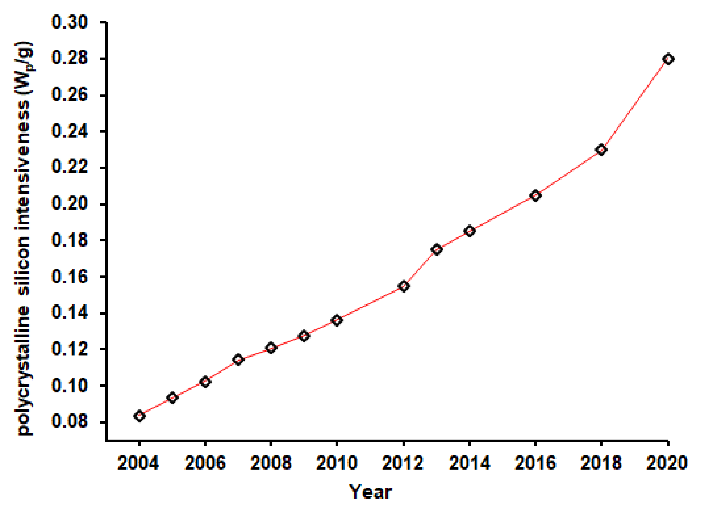
As stated, thin film (CdTe, CIGS) technologies are limited in production due to limits in material sources [
20]. Crystalline silicon cells and modules are expected to continue in their “work horse” position. Through technology development, the effective use of starting polycrystalline silicon material was achieved, as demonstrated in
Figure 16, and the energy return on investment (EROI) of PV systems with PERC modules is higher than 15, worldwide [
10].
Although the impact of increasing efficiency, reducing prices, and extending the life of PV modules on the LCOE is gradually decreasing (see
Section 2), photovoltaic systems are considered a very important part of the future energy sector [
63]. Some scenarios expect the PV module’s annual production to be over 1 TW
p after 2030 [
27]. In some scenarios, a technological transition from P-type to N-type starting wafers [
26,
27,
31,
64] is expected. This transition could increase the efficiency of the modules from 20% to 23%, which may reduce (calculated according to Equation (5)) the area-dependent investment costs by 8.7%, which may be particularly interesting for projects with a high share of area-dependent costs. On the other hand, an increase in efficiency could also be realized by P-type TOPCon technology [
40], which could be less expensive to invest in.
The current increase in the cost of the construction materials of PV systems (copper, iron, aluminium, etc.) increases the area-related costs, and thus improves the conditions for the use of PV modules with higher efficiency in new projects.
However, there may be certain material limits that affect this development. The limits in material resources have been discussed in detail in [
64]. Resources limit not only the multi-GW scale production of CIGS, but also all types of PV cells using ITO contact layers. Another scarce material used in photovoltaic technologies is silver. Silver consumption for TOPCon cells is 50% higher than for PERC cells; for HJT cells, it is 100% higher than for PERC cells. The increase in the price of scarce materials may slow down the transition from PERC to TOPCon and HJT technologies.
The sources of bismuth used in low temperature soldering in HJT modules are also relatively limited. With the massive expansion of production, it will be necessary to reduce the specific consumption of these materials, or to develop technologies that will replace these rare materials with more affordable ones.


